
Graphene prototype modulator shown working at 10 Gigabit
- Imec's graphene electro-absorption modulator works at 10 Gigabit-per-second
- The modulator is small and has be shown to be thermally stable
- Much work is required to develop the modulator commercially
 Cross-section of the graphene electro-absorption modulator. The imec work was first detailed in a paper at the IEDM conference held in December 2014 in San Francisco. Source: imec
Imec has demonstrated an optical modulator using graphene operating at up to 10 Gigabit. The Belgium nano-electronics centre is exploring graphene - carbon atoms linked in a 2D sheet - as part of its silicon photonics research programme investigating next-generation optical interconnect. Chinese vendor Huawei joined imec's research programme late last year.
Several characteristics are sought for a modulator design. One is tiny dimensions to cram multiple interfaces in as tight a space as possible, as required for emerging board-to-board and chip-to-chip optical designs. Other desirable modulator characteristics include low power consumption, athermal operation, the ability to operate over a wide range of wavelengths, high speed (up to 50 Gbps) and ease of manufacture.
Imec's interest in graphene stems from the material's ability to change its light-absorbing characteristics over a wide spectral range. "Graphene has a high potential for a wide-band modulator solution and also for an athermal design," says Joris Van Campenhout, programme director for optical I/O at imec.
 Source: Gazettabyte
Modulation
For optical modulation, either a material's absorption coefficient or its refractive index is used. Silicon photonics has already been used to implement Mach-Zehnder interferometer and ring resonator modulators. These designs modifying their refractive index and use interference to induce light intensity modulation.
"Mach-Zehnder modulators have been optimised dramatically over the last decade," says Van Campenhout. "They can generate at very high bit rates but they are still pretty big - 1mm or longer - and that prevents further scaling."
Ring resonators are more compact and have been shown working at up to 50 Gigabit. "But they are resonant devices; they are wavelength-specific and thermally dependent," says Van Campenhout. "A one degree change can detune the ring resonance from the laser's wavelength."
The other approach, an electro-absorption modulator, uses an electric field to vary the absorption coefficient of the material and this is the graphene modulator approach imec has chosen.
Electro-absorption modulators using silicon germanium meet the small footprint requirement, have a small capacitance and achieve broadband operation. Capacitance is an important metric as it defines the modulator's maximum data rate as well as such parameters as insertion loss (how many dBs of signal are lost passing through the modulator) and the extinction ratio (a measure of the modulator's on and off intensity).
"Silicon germanium offers a pretty decent modulation quality," says Van Campenhout but the wavelength drifts with temperature. Thermal drift is something that graphene appears to solve.
Imec's graphene electro-absorption modulator comprises a 50 micron graphene-oxide-silicon capacitor structure residing above a silicon-on-insulator rib waveguide. The waveguides are implemented using a 200mm wafer whereas the graphene is grown on a copper substrate before being placed on the silicon die. Van Campenhout refers to the design as hybrid or heterogenous silicon photonics.
The graphene modulator exhibits a low 4dB insertion loss and an extinction ratio of 2.5dB. The device's performance is stable over a broad spectrum: an 80nm window centred around the 1550nm wavelength. The performance of up to 10Gbps was achieved over a temperature range of 20-49°C.
"The key achievement is that we have been able to show that you can operate at 10 Gigabit with very clean modulation eye diagrams," says Van Campenhout. However, much work is needed before the device becomes a viable technology.
 Source: Gazettabyte, imec
What next?
Imec has modelled the graphene modulator using a simple resistor-capacitor circuit. "We have been able to identify sources of capacitance and resistance," says Van Campenhout. "We can now better optimise the design for speed or for efficiency."
The speed of the modulator is dictated by the resistance-capacitance product. Yet the higher the capacitance, the greater the efficiency: the better the extinction ratio and the lower the insertion loss. "So it comes down to reducing the resistance," says Van Campenhout. "We think we should be able to get to 25 Gigabit."
With the first prototype, the absorption effect induced by the electric field is achieved between a single graphene plate and the silicon. Imec plans to develop a design using two graphene plates. "If two slabs of graphene are used, we expect to double the effect," says Van Campenhout. "All the charge on both plates of the capacitor will contribute to the modulation of the absorption."
However the integration is more difficult with two plates, and two metal contacts to graphene are needed. "This is still a challenge to do," says Van Campenhout.
Imec has also joined the Graphene Flagship, the European €1 billion programme that spans materials production, components and systems. "One of the work packages is to show you can process on a manufacturing scale graphene-based devices in a CMOS pilot line," he says. Another consideration is to use silicon nitride waveguides rather than silicon ones as these can be more easily deposited.
One challenge still to be overcome is the development of an efficient graphene-based photo-detector. "If this technology is ever going to be used in a real application, there should be a much more efficient graphene photo-detector being developed," says Van Campenhout.
Huawei joins imec to research silicon photonics
Huawei has joined imec, the Belgium nano-electronics research centre, to develop optical interconnect using silicon photonics technology. The strategic agreement follows Huawei's 2013 acquisition of former imec silicon photonics spin-off, Caliopa.
 Source: Gazettabyte
“Having acquired cutting-edge expertise in the field of silicon photonics thanks to our acquisition of Caliopa last year, this partnership with imec is the logical next move towards next-generation optical communication,” says Hudson Liu, CEO at Huawei Belgium.
Imec's research focus is to develop technologies that are three to five years away from production. "Imec works with leading IC manufacturers and fabless companies in the field of CMOS fabrication," says Philippe Absil, department director for 3D and optical technologies at imec. "One of the programmes with our co-partners is about optical interconnect and silicon photonics, and Huawei is one of the participating companies."
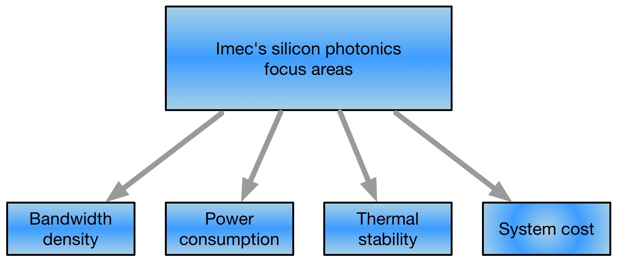
Imec's research concentrates on board-to-board and chip-to-chip interconnect. The optical interconnect work includes increasing interface bandwidth density, reducing power consumption, and achieving thermal stability and system-cost reduction.
The research centre has demonstrated high-bandwidth interfaces as part of work with Chiral Photonics that makes multi-core fibre. Imec has developed a 2D ring of grating couplers that allow coupling between the silicon photonics chip and Chiral's 61-core fibre. "A grating coupler is a sub-wavelength structure that diffracts the light from a waveguide in a vertical direction towards the fibre above the chip," says Absil. This contrasts to traditional edge coupling to a device, achieved by dicing or cleaving a facet on the waveguide, he says.
Another research focus is how to reduce device power consumption and achieve thermal stability. One silicon photonics component that dictates the overall power consumption is the modulator, says Absil. "The Mach-Zehnder modulator is known to consume significant amounts of power for chip-to-chip distances," he says. "The alternative is to use resonating-based modulators but these have to be thermally controlled, and that has an associated power consumption."
Imec is looking at ways to reduce the thermal control needed and is investigating the addition of materials to silicon to create resonator modulators that do away with the need for heating.
The system-cost reduction work looks at packaging. "Eventually, we want to get the optical transceiver inside a host IC," says Absil. "That package has to enable an optical pass-through, whether it is fibre or an optically-transparent package." Such a requirement differs from established CMOS packaging technology. "The programme is also looking to explore new types of packaging for enabling this optical pass-through," he says.
Absil says certain programme elements are two years away from being completed. "In the programme, we have topics that are closer to being adopted and some that are further away, maybe even to 2020."
Multi-project wafer service
Imec is part of the a consortium of EC research institutes that provide low-cost access to companies that don't have the means to manufacture their own silicon photonics designs. Known as Essential, the EC's Seventh Framework (FP7) programme is an extension of the ePIXfab silicon photonics multi-project wafer initiative. "Imec is offering one flavour of the technology, Leti is also offering a flavour, and then there is IHP and VTT," says Absil. Once the Essential FP7 project is completed, the service will be continued by the Europractice IC service.
Has imec seen any growth now that the funding for OpSIS, the multi-project wafer provider, has come to an end? "We see decent contributions but I wouldn't say it is exponential growth," says Absil, who notes that the A*STAR Institute of Microelectronics in Singapore that OpSIS used continues to offer a multi-project wafer service.
Status of silicon photonics
Despite announcements from Acacia and Intel, and Finisar revealing at ECOC '14 that it is now active in silicon photonics, 2014 has been a quiet year for the technology.
"Right now it is a bit quiet because companies are investing in development," says Absil. "There is not so much incentive to publish this work." Another factor he cites for the limited news is that there are vertically-integrated vendors that are putting the technology in their servers rather than selling silicon-photonics products directly.
"This is only first generation," says Absil. "As it picks up, there will be more incentive to work on a second generation of silicon photonics which will depart from what we know from the early work published by Intel and Luxtera."
The opportunities this next-generation technology will offer are 'quite exciting', says Absil.