
imec's novel ADC promises faster sampling rates
The analogue-to-digital and digital-to-analogue converters (ADCs/DACs) are like the equals sign in mathematics.
The equals sign is taught as showing two sides of an equation being the same. But really, it is a gateway between two worlds. The same applies to the ADC and DAC, which equate between the analogue and digital worlds.
Progress in wireline communications, whether client-side optics or coherent optical modems at 800 gigabits and soon 1.6 terabits, means converters must sample at higher rates.
In February, at the IEEE International Solid-State Circuits Conference (ISSCC) in San Francisco, imec detailed a proof-of-concept chip design that promises to advance high-speed ADCs.
In the paper, the authors from the Belgium nano and digital technology innovation centre detailed a 16nm CMOS 7-bit ADC test chip operating at 42 Giga-samples per second (GSps). The speed is not particularly noteworthy, but the design is: a tiny ADC circuit that promises future faster designs.
imec believes a 250-300GSps ADC will be possible when implemented in a state-of-the-art 2nm or 3nm CMOS process.
Converters for comms
I am text block. Click edit button to change this text. Lorem ipsum dolor sit amet, consectetur adipiscing elit. Ut elit tellus, luctus nec ullamcorper mattis, pulvinar dapibus leo.
Time-interleaved SAR
For such high-speed ADCs, a time-interleaved successive approximation register (SAR) architecture is commonly used. The converter design is relatively small and power efficient. Van Driessche says imec has almost two decades of experience designing such ADCs.
The time-interleaved refers to the sampled high-speed signal being distributed across parallel ADC channels. Van Driessche cites as an example a 100GSps ADC that distributes the samples to 100 such interleaved channels, each operating at 1GSps.
“The input [to the ADC] is still operating at full speed, but your ADCs, or channels, operate at a hundredth of the speed,” says Van Driessche.
The issue with a time-interleaved SAR-based converter is that as the speed increases, so does size. The result is longer interconnect lines linking the channels and distributing the clocking signal.
“Distributing the signal and the clock over long lines leads to large parasitics,” says Van Driessche. And with parasitics comes a higher power consumption and/or a lower overall analogue bandwidth.
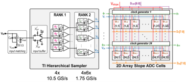
imec’s ISSCC ADC (see diagram) simplifies the SAR circuitry. Dubbed a time-interleaved slope ADC, each channel is even slower than the traditional design. But the primary circuit is tiny, comprising a sampling switch, sampling capacitor, comparator, and a few digital gates. Reducing its size and arranging multiple such units in a 2D array shortens the interconnects, lowering the power and widening the circuit’s bandwidth.
The result is a compact design and a much-reduced power consumption. “This is the essence: to make the core of the ADC significantly smaller, smaller than any alternative that we are aware of,” says Van Driessche.
5nm CMOS design
The ISSCC paper reports the results of a 16nm test chip operating at 42GSps. “You first need to prove that it works,” says Van Driessche. The core’s area is 0.07mm2 only.
Now, imec is working on a 5nm CMOS version. The smaller and faster transistors help achieve higher sampling rates and better power efficiency. But it also comes with challenges: much more impact from parasitics limiting the analogue bandwidth and the resulting speed, and obtaining sufficient output voltage swing at low-power consumption for the DAC.
“The real benefit of the novel ADC architecture comes when you go to higher sampling rates,” says Van Driessche. imec is not saying how fast, but it expects it to exceed 150GSps significantly. Imec expects to tape out the ADC alongside an equivalent DAC next month, with measurement results expected by year-end.
Based on simulation results, imec expects to halve the ADC’s power consumption compared to other similar-speed ADCs. Designers get a notable power saving or can use two channels for the same power.
At OFC 2023, Imec detailed how it expects to achieve sampling rates of 250GSps for a 3nm CMOS coherent DSP design.
How much faster can ADCs go?
Van Driessche says that in future, the gains from technology scaling will diminish, requiring very skilled designers and a huge amount of effort.
“At some point, and I cannot say when, there will be diminishing returns,” he says. “We are not there yet, but we are getting closer.”
Once companies decide that a limit is reached, several parallel channels will be needed, a development designers will want to avoid for as long as possible.

Do optical DACs have a role in future coherent modems?
- A proposed optical digital-to-analogue converter (oDAC) concept offers several system benefits, including better signal performance, higher bit rates and lower power consumption.
- The oDAC design benefits coherent optics but can also be used in direct-detect designs. This article focusses on coherent optics.
- Coherent system vendors are aware of oDAC technology but it is not part of their current roadmaps.
Systems vendors continue to advance the performance of optical transmission systems. But they are the first to admit the task is getting more complex.
Long-distance transmission is challenging due to the channel impairments introduced by the optical fibre, such as noise, chromatic dispersion, and non-linearities.
Coherent modems have become the established technology that use a powerful digital signal processor (DSP) and optics to counter channel impairments.
In recent years the industry has progressed coherent technology to such a degree that it is now difficult to keep improving optical performance.
One critical component of the coherent DSP is the analogue front end: the transmitter’s digital-to-analogue converters (DACs) and the receiver’s analogue-to-digital converters (ADCs).
The DACs take the digital signal input and produce the analogue drive signal for the coherent optics’ Mach-Zehnder modulators. In turm, the DSP’s ADCs sample the signal at the receiver’s optics before recovering the transmitted data payload.
The challenge facing coherent DSP designers is to keep scaling the bandwidth of the DACs and ADCs while maintaining high resolution and high energy efficiency.
This growing challenge has led some researchers to propose alternatives.
One such proposal is an optical digital-to-analogue converter or oDAC.
The status of coherent DSPs
Recent announcements from leading coherent optic vendors, including Cisco’s Acacia, Ciena, Infinera, NEL, and Nokia, show the continual progress in hiking the symbol rate of coherent DSPs.

Vendors want to keep increasing the symbol rate – the frequency of the symbols where each symbol carries one or more bits, depending on the modulation scheme used – since it remains the best way to reduce the cost of sending network traffic.
First-generation coherent systems used a symbol of 32 gigabaud (GBd). Now, Acacia’s currently shipping 5nm CMOS Jannu DSP operates at up to 140GBd. Ciena, meanwhile, has detailed its WaveLogic 6 Extreme, the first coherent DSP implemented in 3nm CMOS that will work at up to 200GBd.
To scale the baud rate, all the sub-systems making up the coherent modem must scale.
The sub-systems include the DSP’s DACs and ADCs, the modulator drivers, and the trans-impedance amplifiers. The coherent optics – the coherent driver modulator (CDM) transmitter and the integrated coherent receiver (ICR) – must also scale.
For a 200GBd symbol rate, the bandwidth of all these components must reach 100GHz.
Looking ahead
The industry consensus is that coherent modems will reach 280-300GBd before the decade’s end. But to do so will require considerable engineering effort.
The industry offers less visibility after 300+GBd.
System vendors say that at some future point, it will not make economic sense to keep increasing the baud rate. It will be too costly to make the coherent modem and reducing the cost-per-bit will stop.
Already each new generation CMOS node is more costly while new materials are needed to scale the optics. Ciena says it is using silicon photonics for the integrated coherent receiver, while indium phosphide is being used for the transmitter’s modulators. Ciena is also looking at thin-film lithium niobate as a modulator technology.
As for DACs and ADCs, circuit designers face considerable challenges in achieving a 100GHz bandwidth.
Moreover, the DACs and ADCs sample faster than the baud rate, typically 1.2x. At OFC, imec, the Belgium technology research centre, outlined its work on 3nm coherent DSPs showing a sample rate of 250 giga-samples/s.
Such huge sampling rates explain the interest in optical DACs which can process a high-baud rate signal to generate, using optical parallelism, an ultra-high bit-rate signal based on either multi-level Pulse Amplitude Modulation (PAM) or Quadradure Amplitude Modulation (QAM) signals.
Two prominent professors promoting an optical DAC design are Ioannis Tomkos of the department of electrical and computer engineering at the University of Patras, Greece, and Moshe Nazarathy at the faculty of electrical engineering at the Technion University, Israel.
Limitations of DACs
Tomkos starts by highlighting the shortcomings of conventional DACs.
DACs not only have to operate sampling rates at least as high as the baud rate but they also have a finite resolution. Typically, 6-8 bits are used for coherent designs.
The effective number of bits (ENOB) available are even lower due to the clock jitter when operating the electrical circuits at such high speeds.
The finite effective number of bits limit the use of higher-order modulation schemes. Today, coherent systems use up to 16-ary quadrature amplitude modulation (16-QAM), except for the highest capacity, shortest-distance links.
A second issue is the non-linear nature of the optical modulator’s transfer function. “It’s a sine non-linearity type of response in Mach-Zehnder modulators due to the nature of interference,” says Tomkos.
This requires operating the modulator over a reduced range, the linear region of its transfer function around its biasing voltage.
Such curtailing of the driver saves power but results in ‘modulator loss’; the area occupied by the modulator’s constellation points is less than the ideal available (see top left diagram).
“You not driving the modulator to the limit,” says Tomkos. “Modulation loss can be as high as 9-12dB which impacts signal recovery at the receiver.”
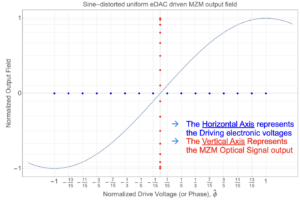
The relation between the driving DAC inputs and the discrete optical outputs is generally nonlinear (see diagram above). This means the constellation points look warped and are not spaced equally apart causing signal distortion.
Such optical distortion can be tackled using various specialised DAC architectures but the cost is either higher power, limited speed or extra modulation loss.
“Ideally, we would like to have equal distances between the symbols so we can robustly separate each symbol from the others since we also have electronic errors coming from the DACs that impact the quality of the symbols and shift them from their optimal points,” says Tomkos.
The impact of modulation loss and optical distortion also worsen when higher modulation schemes above 16-QAM are used.
The oDAC
Mention the term optical DAC, and specific thoughts come to mind. Is the optical signal sampled? Is the DAC electrical in its input and output, but its inner workings are photonic?
The optical DAC, as proposed by Nazarathy and Tomkos, is neither of the above. Moreover, it uses existing driver electronics based on the simplest traditional lowest-order DACs.
Indeed, the oDAC looks similar to a conventional coherent optics transmitter in terms of components, but the differences in operation and achieved performance are significant.
The oDAC can also be implemented in several ways bringing critical benefits for various system requirements.
Architecture
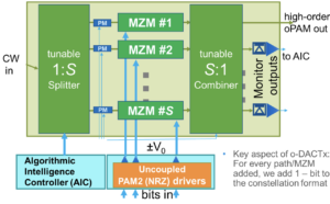
A conventional coherent optical transmitter splits the incoming laser source and feeds the light equally to the in-phase and quadrature Mach-Zehnder modulators (one arm of which includes a 90-degree phase shifter).

The two Mach-Zehnder modulators are driven, as shown. In this example, two drivers implement a bipolar 4-level pulse amplitude modulation (PAM-4) signal such that the coherent transmitter produces a 16-QAM output signal.
The oDAC architecture is subtly different.
The oDAC’s main two components are a variable splitter and combiner at the input and output and the Mach-Zehnder modulator pair. Here, both modulators are identical; there is no 90o phase shifter but the differential phase is maintained at 0o degrees and the modulators are operated at full-scale resulting in zero modulation loss (see diagram at the article’s start).

Each modulator arm is driven by an electrical PAM-4 signal, and the variable splitter-combiner produces the bipolar PAM-16 optical output.
For 16-PAM, 4/5 of the laser signal is fed to one arm and the remaining 1/5 to the other. The PAM-4 DAC drivers for both Mach-Zehnder modulators are identical.
“In the first case, we had 16 symbols in two dimensions (i.e. QAM16); here we have 16 symbols, but in one dimension (i.e. PAM16), the other dimension is missing due to the absence of the 90-degree phase shifter,” says Tomkos.
According to Tomkos, the sine nonlinearity of the optical modulators here is an advantage. “The generated signal does not suffer from modulation loss and optical distortion due to electronic driver mismatch errors, as the noise coming from the electronic DACs gets squelched,” he says.
Higher-order modulation
As mentioned, the oDACs can be implemented and arranged in several ways.
For example, two oDACs can be used, one orthogonal in phase to the other, in a conventional coherent transmitter structure to generate a higher modulation signal. For example, two optical DAC arms, each 16-PAM, used as I and Q, will produce a 256-QAM signal.
But even more strikingly, more than two parallel modulation paths (by stacking-up more modulators in parallel, see diagram) can be used as an alternative approach to generating higher-order modulation schemes and higher bit rates, and at reduced power consumption per bit.
“The ratio between the bit rate and the baud rate is exactly the number of parallel paths,” says Nazarathy. “Another name for it is spectral efficiency: how many bits each symbol carries.”
The oDAC uses straightforward drivers. The professors say only PAM-2 or PAM-4 drivers are used. This way, power savings are maximised.
“The big picture is that we offload the electronics burden by going parallel optically,” says Nazarathy, adding that what is being traded is electronic DAC complexity and the associated performance limitations of the drivers for optical parallelism of replicated blocks of Mach-Zehnder modulators.
“You don’t want to stack things [photonic componentry] serially as if you keep stacking that way, you incur an optical loss because the loss is compounded,” says Nazarathy. Here, the modulators are stacked in parallel, the preferred integration approach.
Moreover, the more paths used, the higher-order the generated optical constellation is. “Eventually, only PAM-2 (Non-return-to-zero) drivers are used and that’s the minimum power consumption you can get,” says Tomkos.
“So we have parallelism (at the same laser power) that generates for the same baud rate, double or triple the bit rate [depending on whether 2 or 3 paths are used],” says Nazarathy. And the resulting constellations are near ideal: there is no modulation loss, nor is there optical distortion.
Nazarathy explains such benefits as the result of a ‘divide-and-conquer’ approach.
“If you keep the modulation paths simple, you have more freedom to optimise the drive point of the modulators,” he says. “The modulators benefit you more because they are more simply driven.” Then, by adding more modulator paths, the system performance improves overall.”
He also notes how the optical implementation is robust to imperfections generated by the electronic circuitry.
Optical DAC: A definition
- Two or more optical modulator units and some static or slowly-tuned ‘glue’ optics.
- The electrical drivers feeding the optical modulators are simple for lowest-power, either PAM2 (NRZ) or PAM4 drivers. Electronic DACs generating higher-order PAM are not needed.
- No high-speed power-hungry digital encoder (mapper) is used. The number of Mach-Zehnder modulators is B where the constellation size is C=2B. This is referred to as Direct Digital Drive. This last condition ensures the lowest power consumption.
Status
The oDAC work is currently at the research stage.
The working of the oDAC has been simulated and verified, and several papers have been published. Patents have also been filed.
At the recent OFC event in San Diago in March, Professor Tomkos met with hyperscalers, systems and components vendors to explain the oDAC technology and its benefits.
The two academics are focused on the oDAC in the optical transmitter, but Nazarathy says they also plan to surprise at the optical receiver end.
Tomkos says the optical DAC is an ideal fit for future coherent transmitters that will be used in 6G networks and datacenter networks, which will carry significant amounts of traffic at ultra-high rates.
The oDAC approach also bodes well for the trend of using linear drive optics. Indeed, the implementation of the oDAC hardware is carried out within the framework of a major R&D project called FLEX-SCALE that Tomkos is co-ordinating and is funded under the first phase of the 6G Smart Networks and Services (SNS) Partnership.
Tomkos believes that the first use of the optical DAC may likely be for data centre interconnect, a more mature market where higher-order modulation formats can be used and low-power is at a premium.
The professors are looking for partners and exploring options to commercialise the technology.

imec’s research work to advance biosensors

Part 3: Biosensor developments
- Pol Van Dorpe discusses the institute’s use of photonics and silicon to develop new designs for medical diagnostics.
- imec has designed a breathalyser that detects the coronavirus with the accuracy of a polymerase chain reaction (PCR) test, a claimed world first.
Optics and photonics are advancing medical diagnostics in two notable ways.
The technologies are helping to shrink diagnostic systems to create new types of medical devices.
“Going from big lab equipment to something much smaller is a clear trend,” says Pol Van Dorpe, a Fellow at imec, the Belgium R&D nanoelectronics and nanotechnology institute.
Photonics and silicon also benefit central labs by creating more powerful test instruments. More functionality and detectors can be integrated in a given area enabling multiple tests in parallel, a technique dubbed multiplexing.
imec’s biosensor work and espertise
imec began its biosensor research in the 1990s, investigating electrical and surface plasmon-based devices. In more recent years, it has added the development of custom biosensor chips for companies.
As examples, imec worked with Panasonic to develop a chip for PCR, a testing technique now known to the public due to covid-19. The R&D institute also worked with Genalyte, a pioneering silicon photonics medical diagnostics company that uses optical waveguides, ring resonators, and a tunable laser for its multiplexing biosensor product.
imec has also developed in-house expertise across several disciplines needed for biosensor development.
Several groups at imec cover photonics, with Van Dorpe heading the group addressing biophotonics and single-molecule electrical devices.
Another group addresses biochemistry and surface chemistry used to coat and activate a sensor’s surface so that receptors can be attached. Receptors are biochemical materials that enable the sensor to trap and detect materials.
A further team covers microfluidics used to deliver liquid samples to the sensor or to mix solutions precisely.
Semiconductor process steps are used to create high-aspect-ratio structures that implement microfluidic structures. Such structures can also be used to sort cells, known as cytometry.
“There are many sensor types, and each has its own fluidic needs,” says Van Dorpe.
Spin-offs
imec has also spun off several biosensor companies.
One, miDiagnostics, raised $16.5 million in funding in 2020. miDiagnostics has a nanofluidic processor (nFP) that performs diagnostic tests on fluids guided through the system using capillary forces. The liquids can be redirected and can even have their flow reversed.
The nFP is configurable depending on the application. It combines nanofluidic processing and PCR for processing biomarkers: from cells and proteins to nucleic acids and small molecules.
Indigo is another spin-off that is developing a glucose monitoring system. A photonics sensor is embedded under the skin and communicates the user’s blood sugar level to a smartphone.
Market trends
The biosensor market is complex. Many actors – labs, doctors and users – in healthcare must be convinced before adopting a biosensor device. For a device to be successful, it must add value compared to existing equipment. Cost is also key as is the use-case and ease of use.
Portable equipment that delivers results promptly so that medical staff can make quick decisions is one example. Others include identifying if a patient has suffered a heart attack or bacterial infections such as sepsis, or enabling a doctor’s office to determine if a patient has a bacterial or viral infection. But no doctor will have 20 devices in their office, each performing a specific test, he says.
Such biosensor devices could also have played a key role during the current coronavirus pandemic.
“I can tell you we were working with companies and if they were several years ahead in their roadmaps, much of this would have been a lot easier,” says Van Dorpe.
Antigen-based quick tests for covid exist but people don’t trust them completely due to their limited sensitivity. It is also still not known when people become contagious. “If you take a nasal swab but are already recovering then you may not be as contagious,” says Van Dorpe.
imec has developed a coronavirus breathalyser. Blowing into a filter, aerosols and small droplets from a person’s lungs are collected. A 5-minute PCR analysis unit delivers a result, informing the person if their breath is infectious.
The goal is to use such systems at airports and large events, but it doesn’t guarantee that a person won’t get sick. “You could have been infected the previous day,” says Van Dorpe.
In clinical trials with UZ Leuven, the university hospital of Leuven, the system has tested viral RNA in exhaled air with high sensitivity.
“Our chip technology can detect quickly the virus particles with the same accuracy as classical PCR tests,” says Van Dorpe. “We are the first in the world to demonstrate this.”
imec is undertaking more clinical trials while improving the test’s robustness and ease of use. “We are discussing the commercialisation of our technology with different parties,” he says.
Biosensor technologies
imec’s toolbox of technologies include silicon nitride optical waveguides, beam splitters, filters, spectrometers, and in-plane and out-of-plane lenses.
imec can deposit waveguides on CMOS and has exploited the technique with CMOS image sensors that have many detectors. “We can use commercial image-sensor wafers and deposit the waveguide technology and use those pixels as detectors,” says Van Dorpe.
Established diagnostic techniques used in medical labs include ELISA, a reference technique to detect proteins, and PCR that tests for nucleic acid detection (DNA/ RNA).
The importance of both lab techniques will not change anytime soon, says Van Dorpe.
One reason why ELISA and PCR are so established is that they use ‘amplification’ to detect minute amounts of the material being tested for – the analyte – in complex samples.
For amplification, another label is used in addition to the receptors. The analyte is attached to an antibody within the label, and it is this second label that provides greater testing sensitivity. This, however, requires sample preparation by trained staff.
In contrast, newer biosensors technologies such as surface plasmon resonance (SPR) and silicon photonics use a label-free approach that does away with the second analyte-label stage.
But the label-free sensor is less sensitive; the technique measures when something attaches to the receptors but it can’t distinguish what it measures.
Van Dorpe stresses that amplification is chemistry-related and so it can be used with silicon photonics or SPR.
It is the overall diagnostic system that determines sensitivity, the combination of the transduction process and the chemistry, says Van Dorpe.
SPR and silicon photonics
SPR and silicon photonics biosensors work by measuring changes in light caused by passing a sample over the sensor which causes molecules to attach to the surface.
An SPR system comprises a laser, a prism attached to a gold surface, and a detector. Light is shone through the prism and is reflected from the gold layer before being detected. At a certain incident angle, the light causes electron resonance on the gold surface causing the reflected light intensity to dip.
Attaching biochemical receptors to the gold surface tailored to the analyte causes a shift in resonance angle and the angle change is a measure of the analyte’s presence.
In contrast, silicon photonic designs measure refractive index changes in the light caused by analytes attached to receptors on the sensor’s surface. Two sensor designs are used: a laser with either a Mach-Zehnder interferometer (MZI) or a ring resonator.
“Everything that changes the refractive index causes a signal,” says Van Dorpe.
imec’s biosensor developments
imec’s work with Genalyte a decade ago involved a biosensor that used a tunable laser and ring-resonator sensors.
More recently, the R&D institute has developed technologies not reflected in the silicon photonics designs used by biosensor start-ups such as Genalyte, SiDx, Antelope DX and SiPhox.
imec’s biosensor technologies have been developed to be less sensitive to non-specific binding. What is measured is fluorescence that occurs with the binding to the analyte.
“In blood or more complicated samples, there is a lot of stuff [besides what is being tested for],” says Van Dorpe.
One technology imec has developed performs rapid ELISA-style testing without needing the repeated wash stages required with ELISA systems.

ELISA uses an antibody receptor to detect the tested-for material while a second antibody uses an enzyme that produces colour. And it is the colour that is measured. In effect, both antibodies detect the analyte but the second, with its fluorescent label, helps determine how much analyte has bound.
With standard ELISA testing, repeated wash steps are required to remove what has not bound to the receptors and labels. These wash stages lengthen the testing time.
imec’s sensor is sensitive in the region very close to the surface. Measuring the fluorescence near the surface determines its build-up over time (see diagram).
The cleverness of the sensor is that the larger the concentration, the faster the surface fills up, reflected in the rate of change of fluorescence over time.
“You don’t need to wait until everything has stabilised to determine the concentration,” says Van Dorpe. “You can wait, say 2 minutes, measure the slope of the signal and that gives you a direct measure of the concentration.”
The design can be used with blood samples, to measure protein production or proteins that shouldn’t be there.
The sensor allows the real-time measurement of biomarkers, and no wash stages are needed. It also enables a controlled process for the biological production of vaccines or cancer therapy.
The key here is that using waveguides and integrated photonics allows localised sensing.
“Also with waveguide technology, because you route light on a chip, you can address a lot of [sensing] sites at the same time,” says Van Dorpe. “That allows you to measure a lot of spots, what is called multiplexing.”
These are the advantages of integrated photonics: the ability to test in parallel and the precise quantification of concentrations, he says.
imec has developed a second fluorescence technique – called super-critical angled fluorescence – closely related to the first but that does away with the waveguide.
As with the first technique, two antibodies are used, one with a fluorescent label.
By exciting the fluorescent label, light is produced in all directions. If a high-angle beam is used, the light at the surface interface refracts within a critical angle.
A fluorescent molecule close to the surface – less than a wavelength away – emits light into a silicon-oxide material. This helps distinguish molecules far from the surface compared to closer ones.
imec’s compact system filters out fluorescence from labels floating further away while measuring those nearby. This is like what happens with the waveguide of the first technique, where it is routed to the detector. But here the detector is situated underneath to measure the fluorescence. The technique delivers rapid results.
The two imec techniques deliver selective sensing that doesn’t rely on refractive index changes or mass. With the latter techniques, all the signals are picked up: everything that binds, wanted and unwanted materials.
The imec techniques are not perfect. There is some degree of auto-fluorescence but it is low. Also, some antibodies with the label will bind to the surface but that is much smaller than the proteins, says Van Dorpe.
Cytometry
imec is working with Sarcura, a cell therapy firm, on a high-throughput cytometry solution for cell separation. Here photonic integration is used along with a microfluidic solution to measure the cells.
A standard cytometer has a flow of cells and a bank of lasers at multiple wavelengths typically. As the cells pass, they scatter the focused light from the lasers. The scattering is measured while the cells also fluoresce since they are labelled. This allows for cell categorisation.
With cell therapy for cancer treatment, immune cells are grown and need analysing. Another use is identifying tumour cells in the blood.
“There are lots of applications where you want to pick out specific cells, label them, look at their properties and classify,” he says.
Traditional equipment used for these tasks is large and complex, requiring skilled staff.
What silicon photonics and microfluidics allow is the bringing of cells to the channel and, with waveguides, illuminate them and detect them.
The result, says Van Dorpe, is a high-throughput design with many adjacent channels.

Silicon photonics' second wave
Two concentric circles drawn in chalk are shown on-screen. So Professor Roel Baets open his plenary talk at the European Conference on Integrated Optics (ECIO) 2020, asking the online audience what is being shown.

Professor Roel Baets
Suggestions come flooding in: the cross-section of an optical fibre, a silicon wafer, a ring resonator optical component and - the correct answer - a doughnut.
The image is from the front cover of Doughnut Economics: Seven Ways to Think Like a 21st-Century Economist by Kate Raworth, a UK professor of economics.
The author discusses how continual economic growth is out of kilter with the planet’s well-being and details alternative approaches. The “doughnut” represents a sweet-spot region ensuring sustainable growth.
Baets applied the book’s thinking to his plenary talk on the topic of silicon photonics research.
Research perspective
Baets’ research work focusses on the use of silicon photonics for applications other than telecom and datacom.
High-speed transceivers for telecom and datacom continue to drive silicon photonics, creating mature platforms and funding the technology’s development.
The two industries will also continue to drive silicon photonics for the coming decade but the picture is set to change. “There is huge potential for other markets; sensing, life sciences and medical being some of them,” he says.
Baets is director of the multidisciplinary Centre for Nano- and Biophotonics at Ghent University in Belgium. His research group comprises 90 staff, split between Ghent University and imec, the renowned R&D centre. “We are sort of a hybrid unit, part university and part imec,” he says.
His focus on the next wave of silicon photonics is partly due to a long-standing interest in biomedical engineering and because high-speed transceiver research is now mainstream.
“I have a big appetite to do something less evolutionary and more groundbreaking,” he says.
Applying the technology to do something helpful appeals to him: “Diagnosing diseases or for therapy of diseases, I feel that is more relevant.”
Background
Baets received the 2020 John Tyndall Award from The Optical Society (OSA) and the IEEE Photonics Society. The award is for his “seminal research in silicon photonics and for driving the foundry model in this field.”
Baets read electrical engineering at Ghent University where he also earned a masters degree. He gained a second masters at Stanford University in California.
“It sounds redundant but I had the privilege of doing a lot of things in terms of subjects that I hadn’t been able to do at Ghent so it was wonderful,” says Baets.
It was at Stanford that Baets pursued his interest in biomedical engineering. He also ‘fell in love’ with photonics after he met and worked with Joseph Goodman, whom he describes as the father of Fourier optics and statistical optics.
That set the course of his photonics research, while his interest in biomedical engineering remained. “And it [biomedical engineering] has popped up in recent years in combination with photonics,” he says.
Foundry model
Baets compares the progress of silicon photonics with that of the chip industry several decades ago.
In the 1970s, universities undertaking integrated circuit research had clean rooms but the growing sophistication of chip-making meant it became too costly.
“Universities and research groups had to give up having their own fabrication facilities for research,” he says.
The same happened within the chip industry, with few chip firms able to afford clean rooms resulting in the advent of foundries.
Even the semiconductor titan Intel, which built its fortune by leading the chip industry in CMOS process technology, is now considering foundries to make its chips.
A similar model is now playing out with integrated photonics.
>
“I believe the field of silicon photonics is at a pivotal point of change and acceleration.”
“The microelectronics fab is an extremely expensive infrastructure,” says Baets. “Maintaining the process flow for certain platforms that enable you to combine [optical] functions on-chip takes quite a bit of diligence and therefore cost.”
This is why creating ‘open’ mechanisms whereby interested parties can gain access to such technology is so important.
“Even if you don’t have a fab in your backyard, there are places you can go to,” says Baets. “That was the essence behind starting ePIXfab.”
Baets helped found ePIXfab, the first global multi-project wafer service for silicon photonics, in 2006.
The idea of multi-project wafers is to aggregate photonic designs from many different users into one mask set before passing a wafer run through a fab. “Multi-project wafers is a cost-sharing process that is well established in electronics,” he says.
Platforms
The Kate Raworth book on sustainable growth was an eye-opener to many people, says Baets, given the topic was addressed by an economist rather than a climate-change scientist.
“Growth is important but there are other dimensions, and you need to find a sweet spot,” he says. “I couldn’t resist using this for my ECIO talk as a metaphor for the field of silicon photonics.”
Silicon photonics is at a turning point, he says, and it will be interesting to see how the field develops over the next five to ten years in terms of finding a way to create mature platforms serving different applications and markets.
The term platform refers to the entire chain of processes that happen in a microelectronics fab, starting with plain wafers and ending with diced chips.
When Baets talks about mature platforms he is referring to a standardised process flow where the basic components are well defined and where a user has some freedom in how the optical functions are connected. It should also be “open access”, similar to CMOS chip foundries.
The technology used for chip-making - the wafer-level processes and the infrastructure - is hugely expensive yet what it produces - the chips - are ‘insanely cheap’, says Baets
“Because of these special boundary conditions, you have to be careful in the research directions you choose,” he says. ”It doesn’t make sense to embark in a direction where it is hard to imagine how it would fit into a sustainable platform.“
This is the essence of his plenary talk.
For example, several places around the world have created a process flow that combines silicon nitride optical waveguides with standard silicon ones. This has only happened in the last couple of years.
“It is a beautiful example of how you can extend the richness of a platform to another level, thereby serving many new applications and customers,” he says.
Meanwhile, a current focus of academic research concerns ways to add III-V lasers to the silica substrate, what he describes as the Holy Grail of silicon photonics.
Baets stresses that there is huge potential for many different applications in the coming years but that it will only happen if real-world products can be made in places that have mature, open-access platforms.
“This is not entirely trivial as it is expensive to establish such platforms,” he says.
There is also this dream of creating a unified platform that can do everything. But Baets says such a generic platform is unrealistic given the overall range of wavelengths used, for datacom, telecom and the longer wavelengths of infra-red.
“You cannot expect one platform to serve all of these,” says Baets. ”But, equally, if there is too much fragmentation, things will not turn out well,” he says.
Baets is aware of at least 20-30 start-up companies developing silicon photonics products, not for datacom or telecom.
In his plenary talk he listed such applications as neuromorphic computing, quantum computing, virtual reality – augmented reality, environmental sensing such as for gas using mid-infrared, critical infrastructure monitoring, and a variery of medical applications such as biosensors, cardiovascular monitoring, glucose monitoring neurophotonics and optical coherence tomography.
Not all these players will be successful but he does expect silicon photonics chips to be made in volumes that will eclipse telecom and datacom in the next five years or so.
But that brings us back to the issue of platforms. “Can they [designers] do things with the existing platforms or do they need a platform that goes a step further - or three steps further?” he says. “And then that question of a unified platform comes up again.”
Training
Baets is dedicating part of his time to address the issue of training in silicon photonics.
“There is a shortage of people with the skills to do silicon photonics,” he says.
Silicon foundries are full of people that understand electronics devices and there is a need for people that understand photonic devices, which are different.
People are also needed with application skills.
“If you think of medical devices, there is a vast distance between expertise in medical-device companies and expertise in the field of silicon photonics,” says Baets. “So there is a need for a lot of bridging work to make people aware of the potential of photonics in general and silicon photonics in particular.”
This is a role ePIXfab has embraced with training activities to address this need.
Research goals
What would Baets like to witness given another decade of uninterrupted research work?
“It is all about impact,” he says. “You would want to see research work turned into something that, at the end of the day, helps people.”
He has great respect for curiosity-driven research. “Curiosity-driven research is like art,” he says. “It is something that is beautiful if done by people with the right skills and is something that society can afford.”
But he is less attracted to conceptual beauty and more to things that prove helpful: “This whole field is about things that help people, whether that is the internet or a medical device.”
Meanwhile, there is COVID-19 to contend with.
As we complete the interview, Baets has a follow-on online meeting with his students.
And the previous evening he attended his first live concert since the start of the COVID-19 lockdown, given by Belgium jazz pianist, Jef Neve. “It was a privilege and it was very enjoyable,” he says.
Classical music is a passion of Baets and in his youth, he played the piano.
“The number of times I now touch the piano is limited but I have some ambition to take it up again,” he says.
Further Information:
Kim Roberts, 2019 John Tyndall Award winner, click here

Imec eyes silicon photonics to solve chip I/O bottleneck
In the second and final article, the issue of adding optical input-output (I/O) to ICs is discussed with a focus on the work of the Imec nanoelectronics R&D centre that is using silicon photonics for optical I/O.
Part 2: Optical I/O
Imec has demonstrated a compact low-power silicon-photonics transceiver operating at 40 gigabits per second (Gbps). The silicon photonics transceiver design also uses 14nm FinFET CMOS technology to implement the accompanying driver and receiver electronics.
 Joris Van Campenhout“We wanted to develop an optical I/O technology that can interface to advanced CMOS technology,” says Joris Van Campenhout, director of the optical I/O R&D programme at Imec. “We want to directly stick our photonics device to that mainstream CMOS technology being used for advanced computing applications.”
Traditionally, the Belgium nanoelectronics R&D centre has focussed on scaling logic and memory but in 2010 it started an optical I/O research programme. “It was driven by the fact that we saw that electrical I/O doesn’t scale that well,” says Van Campenhout. Electrical interfaces have power, space and reach issues that get worse with each hike in transmission speed.
Imec is working with partner companies to research optical I/O. The players are not named but include semiconductor foundries, tool vendors, fabless chip companies and electronic design automation tools firms. The aim is to increase link capacity, bandwidth density - a measure of the link capacity that can be crammed in a given space - and reach using optical I/O. The research’s target is to achieve between a 10x to 100x in scaling.
The number of silicon photonics optical I/O circuits manufactured each year remains small, says Imec, several thousand to ten thousand semiconductor wafers at most. But Imec expects volumes to grow dramatically over the next five years as optical interconnects are used for ever shorter reaches, a few meters and eventually below one meter.
“That is why we are participating in this research, to put together building blocks to help in the technology pathfinding,” says Van Campenhout.
We wanted to develop an optical I/O technology that can interface to advanced CMOS technology
Silicon photonics transceiver
Imec has demonstrated a 1330nm optical transceiver operating at 40Gbps using non-return-to-zero signalling. The design uses hybrid integration to combine silicon photonics with 14nm FinFET CMOS electronics. The resulting transceiver occupies 0.025 mm2, the area across the combined silicon photonics and CMOS stack for a single transceiver channel. This equates to a bandwidth density of 1.6 terabit-per-second/mm2.
The silicon photonics and FinFET test chips each contain circuitry for eight transmit and eight receive channels. Combined, the transmitter path comprises a silicon photonics ring modulator and a FinFET differential driver while the receiver uses a germanium-based photo-detector and a first-stage FinFET trans-impedance amplifier (TIA).
The transceiver has an on-chip power consumption of 230 femtojoules-per-bit, although Van Campenhout stresses that this is a subset of the functionality needed for the complete link. “This number doesn’t include the off-chip laser power,” he says. “We still need to couple 13dBm - 20mW - of optical power in the silicon photonics chip to close the link budget.” Given the laser has an efficiency of 10 to 20 percent, that means another 100mW to 200mW of power.
That said, an equivalent speed electrical interface has an on-chip power consumption of some 2 picojoules-per-bit so the optical interface still has some margin to better the power efficiency of the equivalent electrical I/O. In turn, the optical I/O’s reach using single-mode fibre is several hundred meters, far greater than any electrical interface.
Imec is confident it can increase the optical interface’s speed to 56Gbps. The layout of the CMOS circuits can be improved to reduce internal parasitic capacitances while Imec has already improved the ring modulator design compared to the one used for the demonstrator.
“We believe that with a few design tweaks we can get to 56Gbps comfortably,” says Van Campenhout. “After that, to go faster will require new technology like PAM-4 rather than non-return-to-zero signalling.”
Imec has also tested four transmit channels using cascaded ring modulators on a common waveguide as part of work to add a wavelength-division multiplexing capability.
Transceiver packaging
The two devices - the silicon photonics die and the associated electronics - are combined using chip-stacking technology.
Both devices use micro-bumps with a 50-micron pitch with the FinFET die flip-chipped onto the silicon photonics die. The combined CMOS and silicon photonics assembly is glued on a test board and wire-bonded, while the v-groove fibre arrays are attached using active alignment. The fibre-to-chip coupling loss, at 4.5dB in the demonstration, remains high but the researchers say this can be reduced, having achieved 2dB coupling losses in separate test chips.
 Source: Imec.
Imec is also investigating using through-silicon vias (TSV) technology and a silicon photonics interposer in order to replace the wire-bonding. TSVs deliver better power and ground signals to the two dies and enable high-speed electrical I/O between the transceiver and the ASIC such as a switch chip. The optics and ASIC could be co-packaged or the transceiver used in an on-board optics design next to the chip.
“We have already shown the co-integration of TSVs with our own silicon photonics platform but we are not yet showing the integration with the CMOS die,” says Van Campenhout. “Something we are working on.”
Co-packaging the optics with silicon will come at a premium cost
Applications
The first ICs to adopt optical I/O will be used in the data centre and for high-performance computing. The latest data centre switch ICs, with a capacity of 12.8 terabits, are implemented using 16nm CMOS. Moving to a 7nm CMOS process node will enable capacities of 51.2 terabits. “These are the systems where the bandwidth density challenge is the largest,” says Van Campenhout.
But significant challenges must be overcome before this happens, he says: “I think we all agree that bringing optics deeply integrated into such a product is not a trivial thing.”
Co-packaging the optics with silicon will come at a premium cost. There are also reliability issues to be resolved and greater standardisation across the industry will be needed as to how the packaging should be done.
Van Campenhout expects this will only happen in the next four to five years, once the traffic-handling capacity of switch chips doubles and doubles again.
Imec has seen growing industry interest in optical I/O in the last two years. “We have a lot of active interactions so interest is accelerating now,” says Van Campenhout.
IoT will drive chip design and new styles of computing
Looking back 20 years hence, how will this period be viewed? The question was posed by the CEO of imec, Luc Van de hove, during his opening talk at a day event imec organised in Tel-Aviv.
For Van den hove, this period will be seen as one of turbulent technological change. “The world is changing at an incredible rate,” he says. “The era of digital disruption is changing our industry and this disruption is not going to stop.”
 Luc Van den hove
It was the Belgium nonoelectronics R&D centre’s second visit to Israel to promote its chip and systems expertise as it seeks to expand its links with Israel’s high-tech industry. And what most excites imec is the Internet of Things (IoT), the advent of connected smart devices that turn data into information and adapt the environment to our needs.
The world is changing at an incredible rate. The era of digital disruption is changing our industry and this disruption is not going to stop
Internet of Things
Imec is focussing on five IoT areas: Smart Health - wearable and diagnostic devices, Smart Mobility which includes technologies for autonomous cars, drones and robots, Smart Cities, Smart Industry and Smart Energy. “In all these areas we look at how we can leverage our semiconductor know-how,” says Van den hove. “How we can bring innovative solutions by using our microchip technology.”
The broad nature of the IoT means imec must form partnerships across industries while strengthening its systems expertise. In healthcare, for example, imec is working with John Hopkins University, while last October, imec completed the acquisition of iMinds, a Belgium research centre specialising in systems software and security.
“One of the challenges of IoT is that there is not one big killer application,” says Van den hove. “How to bring these technologies to market is a challenge.” And this is where start-ups can play a role and explains why imec is visiting Israel, to build its partnerships with local high-tech firms.
Imec also wants to bring its own technologies to market through start-ups and has established a €100 million investment fund to incubate new ideas and spin-offs.
Technologies
Imec’s expertise ranges from fundamental semiconductor research to complex systems-on-chip. It is focussing on advanced sensor designs for IoT as this is where it feels it can bring an advantage. Imec detailed a radar chip design for cars that operates at 79GHz yet is implemented in CMOS. It is also developing a Light Detection and Ranging (LIDAR) chip for cars based on integrated photonics. Future cars will have between 50 to 100 sensors including cameras, LIDAR, radar and ultrasound.
 Imec's multi-project wafers. Source: imec
The data generated from these sensors must be processed, fused and acted upon. Imec is doing work in the areas of artificial intelligence and machine learning. In particular, it is developing neuromorphic computing devices that use analogue circuits to mimic the biological circuitry of the brain. Quantum computing is another area imec has begun to explore.
One of the challenges of IoT is that there is not one big killer application
“There is going to be so much data generated,” says Van den Hove. “And it is better to do it [processing] locally because computation is cheaper than bandwidth.”
Imec envisages a network with layers of intelligence, from the sensors all the way to the cloud core. As much of the data as possible will be processed by the sensor so that it can pass on more intelligent information to the network edge, also known as fog computing. Meanwhile, the cloud will be used for long-term data storage, for historical trending and for prediction using neuromorphic algorithms, says Van den Hove.
But to perform intensive processing on-chip and send the results off-chip in a power-efficient manner will require advances in semiconductor technology and the continuation of Moore’s law.
Moore's law
Imec remains confident that Moore’s law will continue to advance for some years yet but notes it is getting harder. In the past, semiconductor technology had a predictable roadmap such that chip designers could plan ahead and know their design goals would be met. Now chip technologists and designers must work together, a process dubbed technology-design co-optimisation.
Van den hove cites the example of imec’s work with ARM Holdings to develop a 7nm CMOS process node. “You can create some circuit density improvement just by optimising the design, but you need some specific technology features to do that,” he says. For example, by using a self-alignment technique, fewer metal tracks can be used when designing a chip's standard cell circuitry. "Using the same pitch you get an enormous shrink," he says. But even that is not going to be enough and techniques such as system-technology co-optimisation will be needed.
Imec is working on FinFETs, a style of transistor, to extend CMOS processes down to 5nm and then sees the use of silicon nanowire technology - first horizontal and then vertical designs - to extend the roadmap to 3nm, 2.5nm and even 1.8nm feature sizes.
Imec is also working on 3D chip stacking techniques that will enable multi-layer circuits to be built. “You can use specific technologies for the SRAM, processing cores and the input-output.” Imec is an active silicon photonics player, seeing the technology playing an important role for optical interconnect.
Imec awarded Gordon Moore a lifetime of innovation award last year, and Van den hove spent an afternoon at Moore’s home in Hawaii. Van den hove was struck with Moore’s humility and sharpness: “He was still so interested in the technology and how things were going.”
The ecosystem for silicon photonics starts to take shape
Silicon photonics luminaries series
Interview 6: imec - Philippe Absil and Joris Van Campenhout
Imec has a unique vantage point when it comes to the status and direction of silicon photonics.
The Belgium nano-electronics research centre gets to see prototype designs nearing commercialisation due to its silicon photonics integration platform and foundry service. “We allow companies to build prototypes using a robust silicon photonics technology,” says Philippe Absil, department director for 3D and optical technologies at imec.
 Philippe Absil
Imec also works intimately with several partners on longer-term research, one being Huawei. This optical I/O R&D activity is part of imec’s CORE CMOS scaling R&D programme which as well as Huawei includes GlobalFoundries, Intel, Micron, Qualcomm, Samsung, SK Hynix, Sony and TSMC. The research is sufficiently far ahead to be deemed pre-competitive such that all the firms collaborate.
For silicon photonics, the optical I/O research includes optical integration schemes, new device concepts and new materials. “The aim is to bring silicon photonics technology to the next level in order to resolve today’s challenges,” says Absil.
Assured future
Imec is confident about silicon photonics’ future but stresses an ecosystem for the technology needs to be in place first. This means having more than one foundry, suitable equipment to reduce the cost of testing silicon photonics circuits, and developing packaging solutions.
“These elements are being developed and the ecosystem is coming together nicely,” says Joris Van Campenhout, programme director for optical I/O at imec.
Another encouraging sign is the strong industry interest in the technology in the last two years. It was mainly academics that were interested in imec's multi-wafer project service but now there is strong demand from companies as well; companies bringing products to market.
Silicon photonics is not a one-off technology; it has value for several generations
Systems scaling is what gives imec confidence that silicon photonics will not end up a niche technology. “Look at the cloud economy and cloud data centres, these systems need to scale continually,” says Van Campenhout. “A lot of effort is being put into scaling, and interconnect is an essential part of such systems.”
Moreover, there are few technologies to deliver such scalability, which is why many of the bigger systems companies are investing in silicon photonics. “Silicon photonics is not a one-off technology; it has value for several generations," says Van Campenhout. “That is really the potential of silicon photonics and that is where the disruption lies.”
Challenges
One focus for imec and its partners is to reduce the overall insertion loss of silicon photonics circuits for short-reach interconnect applications. Such short-reach links span distances of up to a few meters, a market segment currently addressed using advanced copper cabling or VCSEL-based optical interconnects.
 Joris Van Campenhout
Because of the relatively high insertion loss of silicon photonics designs, it is not possible to achieve a sufficiently low-power consumption for such links. “That is a show-stopper because it prevents us closing link budgets,” says Van Campenhout. A link budget refers to the gain and losses across the elements making up the optical link such as the laser, modulator, optical fibre and receiver circuitry.
In order to drive up volumes, silicon photonics needs to become more competitive at shorter reaches where VCSELs are still the mainstream optical technology
The team is tackling the loss issue on two fronts: reducing the insertion loss between the fibre and the waveguide, and reducing the modulator's insertion loss which still exceeds that of other optical technologies.
“For these two parts of the technology, further improvements are required to reduce the overall losses,” says Van Campenhout. “That will enable us to be competitive at shorter distances.” These are engineering challenges, he stresses, rather than any fundamental problem.
Another silicon photonics research area being explored at imec include edge coupling solutions between the waveguide and fibre. “These can have very low insertions losses - one decibel or lower - and can be polarisation insensitive," says Van Campenhout.
Packaging approaches that have a low insertion loss are also being developed, engineered in a way to enable passive alignment assembly procedures. Passively aligning the laser is a key part of reducing component packaging costs. “Silicon doesn’t have a laser so in the next few years it will continue to require hybrid solutions,” says Van Campenhout. “You need a good way to do passive alignment of laser sources, and also packaged in a way that doesn’t require a hermetic solution.”
These are the challenges facing the industry in the next few years: lowering insertion loss and developing packaging technologies. Overcoming these challenges will mark an important milestone since the total market for silicon photonics can be served with a small number of silicon wafers. “In order to drive up volumes, silicon photonics needs to become more competitive at shorter reaches where VCSELs are still the mainstream optical technology,” says Van Campenhout.
It is not yet mature but there is a broader adoption of a model whereby silicon photonics can be designed by one company and fabricated by another
Value proposition
Overall, silicon photonics faces stiff competition from VCSELs and indium phosphide. The two established optical technologies continue to evolve and benefit from having all the optical functionality in one platform, something that silicon photonics, with its lack of a laser source, can’t match.
But the trend whereby the optical transceiver is coming ever closer to the host IC strengthens silicon photonics’ hand. That is because silicon photonics can be co-packaged with silicon, and can share the same equipment as the two device types - electronic and photonic ICs - are put together.
Absil also highlights how the ecosystem needed for widespread adoption of silicon photonics is taking shape. “It is not yet mature but there is a broader adoption of a model whereby silicon photonics can be designed by one company and fabricated by another,” he says. “The adoption of that will result in a new model for the optical component world.”
Market opportunities
Van Campenhout expects silicon photonics to be a niche technology for 100-gigabit connections in the data centre. This may change as silicon photonics matures but today the market is dominated by III-V technologies, he says.
Applications that require integration density in the form of a large number of parallel high-speed transceivers, and close integration with host ICs is what will drive silicon photonics. Imec cites as an example data centre switches which require a large number of network and backplane interconnects tightly integrated with the switch logic IC. These interconnects will be on-board and eventually on-package optical modules. Silicon photonics is ideally placed to provide a scalable I/O solution for such applications, as channel data rates move to 50 gigabit and beyond, says Van Campenhout.
But if it is going to take several years to resolve the insertion loss issues for short-reach interconnects, this is a market application that will only start driving significant volumes early in the next decade.
The advent of 400 Gigabit Ethernet and perhaps 800 Gigabit Ethernet after that will be another driver in the coming years.
Other emerging markets include sensors. “Mid infra-red for sensing is a very interesting topic with quite some potential,” says Van Campenhout. “But it is not entirely clear what will be the killer application.”
Sensing is a fragmented application area where many technology solutions exist. “It is too early to figure out what applications an optical sensing device would be competitive against incumbent designs.” But the more integration required, the more competitive silicon photonics will become for such applications, he says.
The Internet of Things will also use sensing but this will be an extremely cost-sensitive market.
“It is not entirely clear if optical technology will be able to meet such cost pressures but if it does, it will drive tremendous volumes and help develop an ecosystem around silicon photonics,” says Van Campenhout.
Further reading:
Imec gears up for the Internet of Things economy, click here
Mario Paniccia: We are just at the beginning
 During that time, his Intel team had six silicon photonics papers published in the science journals, Nature and Nature Photonics, and held several world records - for the fastest modulator, first at 1 gigabit, then 10 gigabit and finally 40 gigabit, the first pulsed and continuous-wave Raman silicon laser, the first hybrid silicon laser working with The University of California, Santa Barbara, and the fastest silicon germanium photo-detector operating at 40 gigabit.
It got to the stage where Intel’s press relations department would come and ask what the team would be announcing in the coming months. “ 'Hey guys,' I said, 'it doesn't work that way ' ”.
Since leaving Intel last year, Paniccia has been working as a consultant and strategic advisor. He is now exploring opportunities for silicon photonics but in segments other than telecom and datacom.
“I didn't want to go into developing transceivers for other big companies and compete with my team's decade-plus of development; I spent 20 years at Intel,” he says.
Decade of development
Intel’s silicon photonics work originated in the testing of its microprocessors using a technique known as laser voltage probing. Infra-red light is applied to the back side of the silicon to make real-time measurements of the chip’s switching transistors.
For Paniccia, it raised the question: if it is possible to read transistor switching using light, can communications between silicon devices also be done optically? And can it be done in parallel to the silicon rather than using the back side of silicon?
In early 2000 Intel started working with academic Graham Reed, then at the University of Surrey, and described by Paniccia as one of the world leaders in silicon photonics devices. “We started with simple waveguides and it just progressed from there,” he says.
The Intel team set the target of developing a silicon modulator working at 1 gigahertz (GHz); at the time, the fastest silicon modulator operated at 10 megahertz. “Sometimes leadership is about pushing things out and putting a stake in the ground,” he says.
It was Intel’s achievement of a working 1GHz silicon modulator that led to the first paper in Nature. And by the time the paper was published, Intel had the modulator working at 2GHz. The work then progressed to developing a 10 gigabit-per-second (Gbps) modulator and then broadened to include developing other silicon photonics building-block devices that would be needed alongside the modulator – the hybrid silicon laser, the photo-detector and other passive devices needed for an integrated transmitter.
There is a difference between proving the technology works and making a business out of it
Once 10Gbps was achieved, the next milestone was 20Gbps and then 40Gbps. Once the building block devices achieved operation in excess of 40Gbps, Intel’s work turned to using these optical building blocks in integrated designs. This was the focus of the work between 2010 to 2012. Intel chose to develop a four-channel 40Gbps (4x10 gigabit) transceiver using four-wavelength coarse WDM which ended up working at 50Gbps (4x12.5 gigabit) and then, most recently, a 100Gbps transceiver.
He says the same Intel team is no longer talking about 50Gbps or 100Gbps but how to get multiple terabits coming out of a chip.
Status
Paniccia points out that in little more than a decade, the industry has gone from not knowing whether silicon could be used to make basic optical functions such as modulators and photo-detectors, to getting them to work at speeds in excess of 40Gbps. “I’d argue that today the performance is close to what you can get in III-V [compound semiconductors],” he says.
He believes silicon photonics is the technology of the future, it is just a question of when and where it is going to be applied: “There is a difference between proving the technology works and making a business out of it”.
In his mind, these are the challenges facing the industry: proving silicon photonics can be a viable commercial technology and determining the right places to apply it.
For Paniccia, the 100-gigabit market is a key market for silicon photonics. “I do think that 100 gigabit is where the intercept starts, and then silicon photonics becomes more prevalent as you go to 200 gigabit, 400 gigabit and 1 terabit,” he says.
So has silicon photonics achieved its tipping point?
Paniccia defines the tipping point for silicon photonics as when people start believing the technology is viable and are willing to invest. He cites the American Institute for Manufacturing Integrated Photonics (AIM Photonics) venture, the $610 million public and private funded initiative set up in 2015 to advance silicon photonics-based manufacturing. Other examples include the silicon photonics prototyping service coordinated by nano-electronics research institute imec in Belgium, and global chip-maker STMicroelectronics becoming a silicon photonics player having developed a 12-inch wafer manufacturing line.
Instead of one autonomous LIDAR system in a car, you could have 20 or 50 or 100 sprinkled throughout your vehicle
“All these are places where people not only see silicon photonics as viable but are investing significant funds to commercialise the technology,” says Paniccia. “There are numerous companies now selling commercialised silicon photonics, so I think the tipping point has passed.”
Another indicator that the tipping point has happened, he argues, is that people are not spending their effort and their money solely on developing the technology but are using CMOS processes to develop integrated products.
“Now people can say, I can take this process and build integrated devices,” he says. “And when I put it next to a DSP, or an FPGA, or control electronics or a switching chip, I can do things that you couldn't do next to bulky electronics or bulky photonics.”
It is this combination of silicon photonics with electronics that promises greater computing power, performance and lower power consumption, he says, a view shared by another silicon photonics luminary, Rockley Photonics CEO, Andrew Rickman.
Moreover, the opportunities for integrated photonics are not confined to telecom and datacom. “Optical testing systems for spectroscopy today is a big table of stuff - lasers, detectors modulators and filters,” says Paniccia. Now all these functions can be integrated on a chip for such applications as gas sensing, and the integrated photonics device can then be coupled with a wireless chip for Internet of Things applications.
The story is similar with autonomous vehicle systems that use light detection and ranging (LIDAR) technology. “These systems are huge, complicated, have a high power consumption, and have lots of lasers that are spinning around,” he says. “Now you can integrate that on a chip with no moving parts, and instead of one autonomous LIDAR system in a car, you could have 20 or 50 or 100 sprinkled throughout your vehicle”
Disruptive technology
Paniccia is uncomfortable referring to silicon photonics as a disruptive technology. He believes disruption is a term that is used too often.
Silicon photonics is a technology that opens up a lot of new possibilities, he says, as well as a new cost structure and the ability to produce components in large volume. But it doesn’t solve every problem.
The focus of the optical vendors is very much on cost. For markets such as the large-scale data centre, it is all about achieving the required performance at the right cost for the right application. Packaging and testing still account for a significant part of the device's overall cost and that cannot be forgotten, he says.
Paniccia thus expects silicon photonics to co-exist with the established technologies of indium phosphide and VCSELs in the near term.
“It is all about practical decisions based on price, performance and good-enough solutions,” he says, adding that silicon photonics has the opportunity to be the mass market solution and change the way one thinks about where photonics can be applied.
“Remember we are just at the beginning and it will be very exciting to see what the future holds.”
Imec gears up for the Internet of Things economy
It is the imec's CEO's first trip to Israel and around us the room is being prepared for an afternoon of presentations the Belgium nanoelectronics research centre will give on its work in such areas as the Internet of Things and 5G wireless to an audience of Israeli start-ups and entrepreneurs.
 Luc Van den hove
iMinds merger
Imec announced in February its plan to merge with iMinds, a Belgium research centre specialising in systems software and security, a move that will add 1,000 staff to imec's 2,500 researchers.
At first glance, the world-renown semiconductor process technology R&D centre joining forces with a systems house is a surprising move. But for Van den hove, it is a natural development as the company continues to grow from its technology origins to include systems-based research.
"Over the last 15 years we have built up more activities at the system level," he says. "These include everything related to the Internet of Things - our wireless and sensor programmes; we have a very strong programme on biomedical applications, which we sometimes refer to as the Internet of Healthy Things - wearable and diagnostics devices, but always leveraging our core competency in process technology."
Imec is also active in energy research: solar cells, power devices and now battery technology.
For many of these systems R&D programmes, an increasing challenge is managing data. "If we think about wearable devices, they collect data all the time, so we need to build up expertise in data fusion and data science topics," says Van den hove. There is also the issue of data security, especially regarding personal medical data. Many security solutions are embedded in software, says Van den hove, but hardware also plays a role.
Imec expects the Internet of Things to generate massive amounts of data, and more and more intelligence will need to be embedded at different levels in the network
"It just so happens that next to imec we have iMinds, a research centre that has top expertise in these areas [data and security]," says Van den hove. "Rather than compete with them, we felt it made more sense to just merge."
The merger also reflects the emergence of the Internet of Things economy, he says, where not only will there be software development but also hardware innovation: "You need much more hardware-software co-development". The merger is expected to be completed in the summer.
Internet of Things
Imec expects the Internet of Things to generate massive amounts of data, and more and more intelligence will need to be embedded at different levels in the network.
"Some people refer to it as the fog - you have the cloud and then the fog, which brings more data processing into the lower parts of the network," says Van den hove. "We refer to it as the Intuitive Internet of Things with intelligence being built into the sensor nodes, and these nodes will understand what the user needs; it is more than just measuring and sending everything to the cloud."
Van den hove says some in the industry believe that these sensors will be made in cheap, older-generation chip technologies and that processing will be performed in data centres. "We don't think so," he says. "And as we build in more intelligence, the sensors will need more sophisticated semiconductors."
Imec's belief is that the Internet of Things will be a driver for the full spectrum of semiconductor technologies. "This includes the high-end [process] nodes, not only for servers but for sophisticated sensors," he says.
"In the previous waves of innovation, you had the big companies dominating everything," he says. "With the Internet of Things, we are going to address so many different markets - all the industrial sectors will get innovation from the Internet of Things." There will be opportunities for the big players but there will also be many niche markets addressed by start-ups and small to medium enterprises.
Imec's trip to Israel is in response to the country's many start-ups and its entrepreneurship. "Especially now with our wish to be more active in the Internet of Things, we are going to work more with start-ups and support them," he says. "I believe Israel is an extremely interesting area for us in the broad scope of the Internet of Things: in wireless and all these new applications."
 Herzliya
Semiconductor roadmap
Van den hove's background is in semiconductor process technology. He highlights the consolidation going on in the chip industry due, in part, to the CMOS feature nodes becoming more complex and requiring greater R&D expenditure to develop, but this is a story he has heard throughout his career.
"It always becomes more difficult - that is Moore's law - and [chip] volumes compensate for those challenges," says Van den hove. When he started his career 30 years ago the outlook was that Moore's law would end in 10 years' time. "If I talk to my core CMOS experts, the outlook is still 10 years," he says.
Imec is working on 7nm, 5nm and 3nm feature-size CMOS process technologies. "We see a clear roadmap to get there," he says. He expects the third dimension and stacking will be used more extensively, but he does not foresee the need for new materials like graphene or carbon nanotubes being used for the 3nm process node.
Imec is pursuing finFET transistor technology and this could be turned 90 degrees to become a vertical nanowire, he says. "But this is going to be based on silicon and maybe some compound semiconductors like germanium and III-V materials added on top of silicon." The imec CEO believes carbon-based materials will appear only after 3nm.
"The one thing that has to happen is that we have a cost-effective lithography technique and so EUV [extreme ultraviolet lithography] needs to make progress," he says. Here too he is upbeat pointing to the significant progress made in this area in the last year. "I think we are now very close to real introduction and manufacturing," he says.
We see strong [silicon photonics] opportunities for optical interconnect and that is one of our biggest activities, but also sensor technology, particularly in the medical domain
Silicon Photonics
Silicon photonics is another active research area with some 200 staff at imec and at its associated laboratory at Ghent university. "We see strong opportunities for optical interconnect and that is one of our biggest activities, but also sensor technology, particularly in the medical domain," he says.
Imec views silicon photonics as an evolutionary technology. "Photonics is being used at a certain level of a system now and, step by step, it will get closer to the chip," he says. "We are focussing more on when it will be on the board and on the chip."
Van den hove talks about integrating the photonics on a silicon interposer platform to create a cost-effective solution for the printed circuit board and chip levels. For him, first applications of such technology will be at the highest-end technologies of the data centre.
For biomedical sensors, silicon photonics is a very good detector technology. "You can grow molecules on top of the photonic components and by shining light through them you can perform spectroscopy; the solution is extremely sensitive and we are using it for many biomedical applications," he says.
Looking forward, what most excites Van den hove is the opportunity semiconductor technology has to bring innovation to so many industrial sectors: "Semiconductors have created a fantastic revolution is the way we communicate and compute but now we have an opportunity to bring innovation to nearly all segments of industry".
He cites medical applications as one example. "We all know people that have suffered from cancer in our family, if we can make a device that would detect cancer at a very early stage, it would have an enormous impact on our lives."
Van den hove says that while semiconductors is a mature technology, what is happening now is that semiconductors will miniaturise some of the diagnostics devices just like has happened with the cellular phone.
"We are developing a single chip that will allow us to do a full blood analysis in 10 minutes," he says. DNA sequencing will also become a routine procedure when visiting a doctor. "That is all going to be enabled by semiconductor technology."
Such developments is also a reflection of how various technologies are coming together: the combination of photonics with semiconductors, and the computing now available.
Imec is developing a disposable chip designed to find tumour cells in the blood that requires the analysis of thousands of images per second. "The chip is disposable but the calculations will be done on a computer, but it is only with the most advanced technology that you can do that," says Van den hove.
Monolithic silicon photonic chips move a step closer
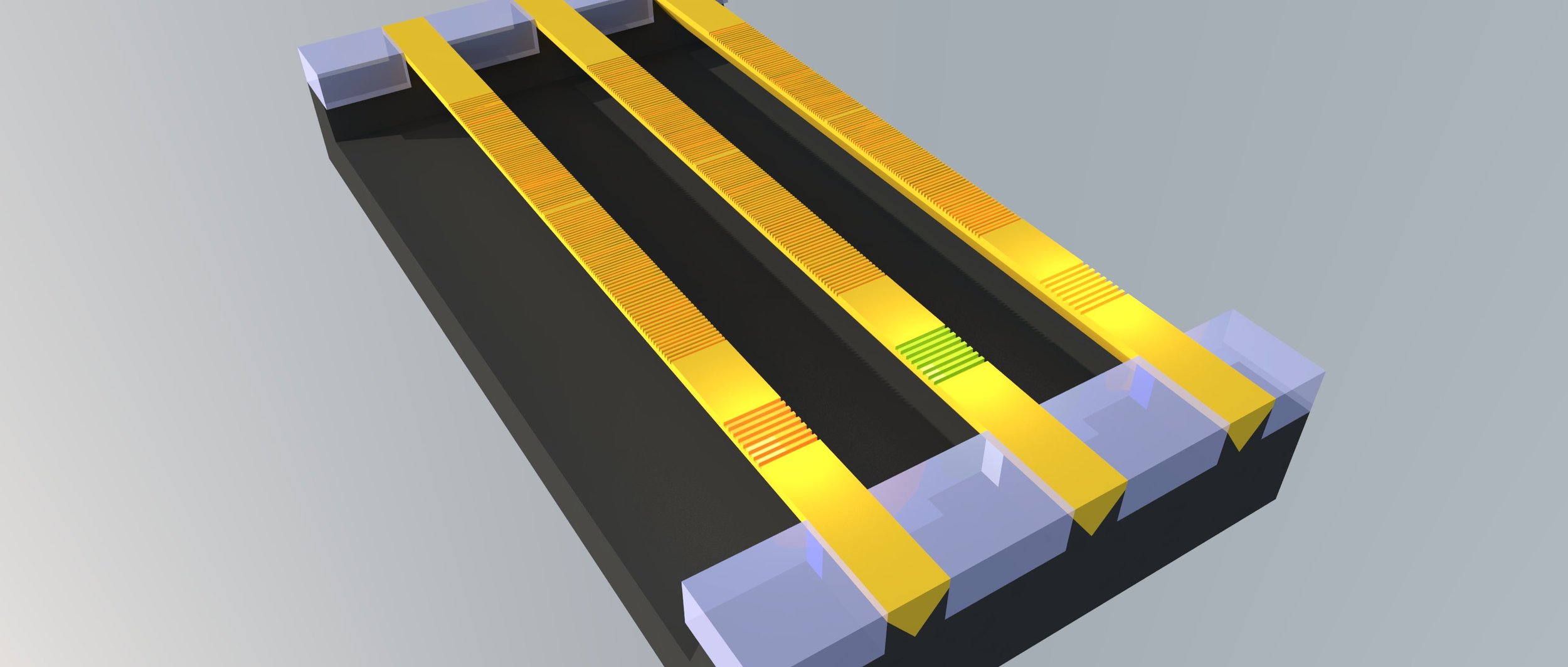 Shown are three v-shaped indium phosphide lasers and their gratings on a silicon-on-insulator substrate. Source: Ghent University, imec
Silicon photonics chips are hybrid designs because of silicon’s inability to generate light. Silicon photonics companies either couple a discrete laser to a chip or bond indium phosphide wafers or ‘chiplets' to the silicon wafer and process it to create working lasers that become part of the silicon photonics chip. Growing lasers directly on silicon creates a third approach for the densest applications.
“Monolithic integration offers the best scalability once you can grow III-V [material] and do wafer-scale processing,” says Professor Dries Van Thourhout of Ghent University. “But it is also the most challenging to implement in terms of pure physics.”
Depositing indium phosphide on a silicon wafer is challenging because differences in the two crystal materials causes defects. Imec and Ghent University have not stopped such defects but has confined them by depositing indium phosphide in pre-etched v-shaped grooves.
The defects propagate along the v-groove and are confined to a layer 20 nm thick compared to alternative approaches that grow the indium phosphide across a wafer where defects propagate several microns deep. The bulk of the deposited material is of high quality, says Van Thourhout.
 Close-up of indium phosphide deposited in the v-groove etched into the silicon wafer. Source: Ghent University, imec.
The challenge is that the amount of indium phosphide material available overall is far less, since the v-groove slots are 300 to 500 nm wide only. “We have these [narrow] slots and we have to adapt the laser design accordingly,” says Van Thourhout.
Ghent University uses the indium phosphide-deposited wafers made on imec’s 300 mm wafer pilot line and etches gratings on top to create the working lasers.
A 20mW external pump laser is used to get the array to lase, says Van Thourhout, while the output power of each laser in the array is 10 mW. The lasers operate in the 910 nm to 930 nm region.
Monolithic integration offers the best scalability once you can grow III-V [material] and do wafer-scale processing. But it is also the most challenging to implement in terms of pure physics
Future work
To get the lasers to work at 1,300 nm and 1,550 nm telecom wavelengths, another material such as indium gallium arsenide will need to be grown on top of the indium phosphide, an area Van Thourhout and his team are investigating.
However, the main challenge still remaining is to use electronic injection to drive the lasers. This requires a PIN junction to be integrated on-chip to inject carriers into the laser, and that will require adding electrical contacts which must not induce optical loss in the laser.
“That will certainly be a design challenge, getting the right doping level and so on,” says Van Thourhout. “We also have to find a way to inject current into the device without disturbing the optical field.” Only then can the reliability of laser array be determined. “That [reliability] is something that at this point is unknown but is very important for any commercial device,” he says.
Ghent University says the optically pumped lasers have not shown any breakdown and almost all the devices tested are operating well but he admits that the work remains preliminary.
Applications
Ghent University says the advent of monolithic lasers will complement existing discrete laser and hybrid techniques rather than replace them.
“The main target for monolithic is high-volume applications and more integrated designs,” says Van Thourhout. One example is optical links between a CPU and memory. Such designs that integrate optics with ICs will have to be very cheap. “The only way to make something like this very cheap is by a very high degree of integration,” says Van Thourhout.
Meanwhile, Imec has a R&D programme on optical I/O with key partners of its core CMOS programmes. Huawei has been one known partner but others include GlobalFoundries, Intel, Micron, Panasonic, Qualcomm, Samsung, SK Hynix, Sony and TSMC.