
Drut tackles disaggregation at a data centre scale
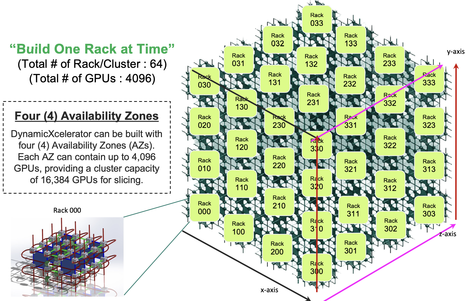
- Drut’s DynamicXcelerator supports up to 4,096 accelerators using optical switching and co-packaged optics. Four such clusters enable the scaling to reach 16,384 accelerators.
- The system costs less and is cheaper to run, has lower latency, and better uses the processors and memory.
- The system is an open design supporting CPUs and GPUs from different vendors.
- DynamicXcelerator will ship in the second half of 2024.
Drut Technologies has detailed a system that links up to 4,096 accelerator chips. And further scaling, to 16,384 GPUs, is possible by combining four such systems in ‘availability zones’.
The US start-up previously detailed how its design can disaggregate servers, matching the processors, accelerators, and memory to the computing task at hand. Unveiled last year, the product comprises management software, an optical switch, and an interface card that implements the PCI Express (PCIe) protocol over optics.
The product disaggregates the servers but leaves intact the tiered Ethernet switches used for networking servers across a data centre.
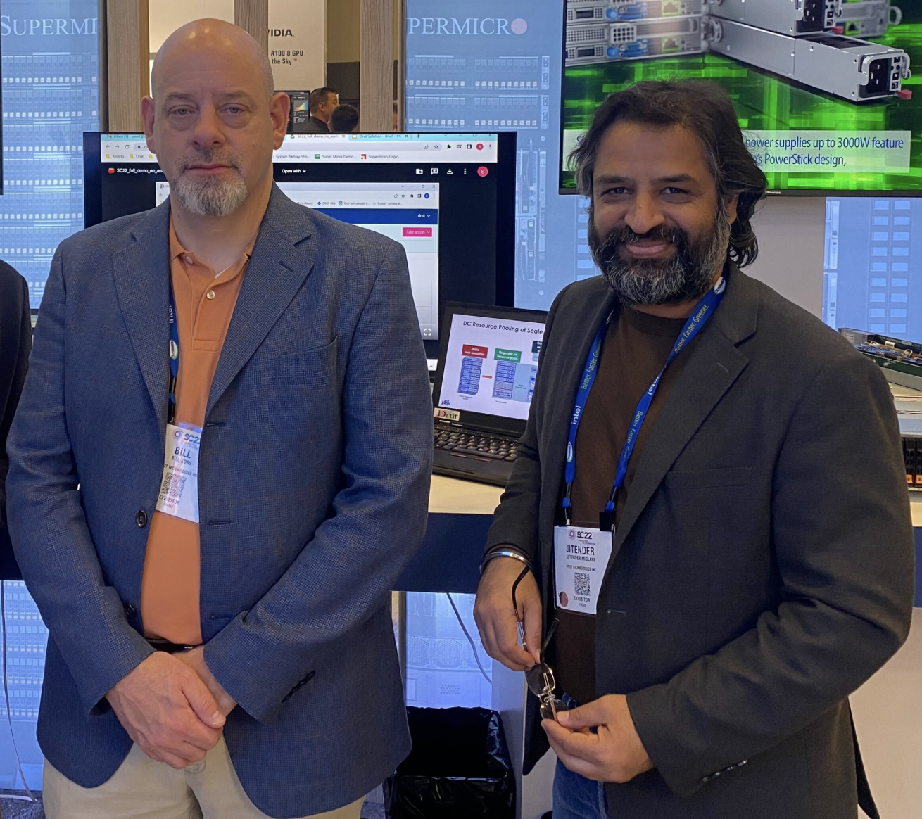
Now the system start-up is expanding its portfolio with a product that replaces the Ethernet switches with optical ones. “You can compose [compute] nodes and drive them using our software,” says Bill Koss, CEO of Drut.
Only Google has demonstrated the know-how to make such a large-scale flexible computing architecture using optical switching.
Company background
Drut was founded in 2018 and has raised several funding rounds since 2021.
Jitender Miglani, founder and president of Drut, previously worked at MEMS-based optical switch maker, Calient Technologies.
Drut’s goal was to build on its optical switching expertise and add the components needed to make a flexible, disaggregated computing architecture. “The aim was building the ecosystem around optical switches,” says Miglani.
The company spent its first two years porting the PCIe protocol onto an FPGA for a prototype interface card. Drut showcased its prototype product alongside a third-party optical switch as part of a SuperMicro server rack at the Supercomputing show in late 2022.
Drut has spent 2023 developing its next-generation architecture to support clusters of up to 4,096 endpoints. These can be accelerators like graphics processing units (GPUs), FPGAs, data processing units (DPUs), or storage using the NVM Express (nonvolatile memory express).
The architecture, dubbed DynamicXcelerator, supports PCIe over optics to link processors (CPUs and GPUs) and RDMA (Remote Direct Memory Access) over optics for data communications between the GPUs and between the CPUs.
The result is the DynamicXcelerator system, a large-scale reconfigurable computing for intensive AI model training and high-performance computing workloads.
DynamicXcelerator
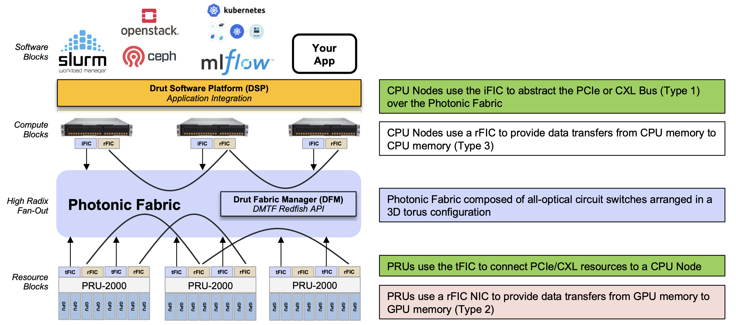
The core of the DynamicXcelerator architecture is a photonic fabric based on optical switches. This explains why Drut uses PCIe and RDMA protocols over optics.
Optical switches brings size and flexibility and by relaying optical signals, their ports are data-rate independent.
Another benefit of optical switching is power savings. Drut says an optical switch consumes 150W whereas an equivalent-sized packet switch consumes 1,700W. On average, an Infiniband or Ethernet packet switch draws 750W when used with passive cables. Using active cables, the switch’s maximum power rises to 1,700W. “[In contrast], a 32-64-128-144 port all-optical switch draws 65-150W,” says Koss.
Drut also uses two hardware platforms. One is the PCIe Resource Unit, dubbed the PRU-2000, which hosts eight accelerator chips such as GPUs. Unlike Nvidia’s DGX platform, which uses Nvidia GPUs such as the Hopper, or Google, which uses its TPU5 tensor processor unit (TPU), Drut’s PRU-2000 is an open architecture and can use GPUs from Nvidia, AMD, Intel, and others. The second class of platform is the compute node or server, which hosts the CPUs.
DynamicXcelerator’s third principal component are the FIC 2500 interface cards.
The iFIC 2500 card is similar to Drut’s current product’s iFIC 1000, which features an FPGA and four QSFP28s. However, the iFIC 2500 supports the PCIe 5.0 generation bus and the Compute Express Link (CXL) protocols. The two other FIC cards are the tFIC 2500 and rFIC 2500.
“The iFIC and tFIC are the same card, but different software images,” says Koss. “The iFIC fits into a compute node or server while the tFIC fits into our Photonic Resource Unit (PRU) unit, which holds GPUs, FPGAs, DPUs, NVMe, and the like.”
The rFIC provides RDMA over photonics for GPU-to-GPU memory sharing. The rFIC card for CPU-to-CPU memory transfers is due later in 2024.
Miglani explains that PCIe is used to connect the GPUs and CPUs, but for GPU-to-GPU communication, RDMA is used since even PCIe over photonics has limitations.
Certain applications will use hundreds and even thousands of accelerators, so a PCIe lane count is one limitation, distance is another; a 5ns delay is added for each metre of fibre. “There is a window where the PCIe specification starts to fall off,” says Miglani.
The final component is DynamicXcelerator’s software. There are two software systems: the Drut fabric manager (DFM), which controls the system’s hardware configuration and traffic flows, and the Drut software platform (DSP) that interfaces applications onto the architecture.
Co-packaged optics
Drut knew it would need to upgrade the iFIC 1000 card. DynamicXcelerator uses PCIe 5.0, each lane being 32 gigabit-per-second (Gbps). Since 16 lanes are used, that equates to 512 gigabits of bandwidth.
“That’s a lot of bandwidth, way more that you can crank out with four 100-gigabit pluggables,” says Koss, who revealed co-packaged optics will replace pluggable modules for the iFIC 2500 and tFIC 2500 cards.
The card for the iFIC and tFIC will use two co-packaged optical engines, each 8×100 gigabits. The total bandwidth of 1.6 terabits – 16×100-gigabit channels – is a fourfold increase over the iFIC 1000.
System workings
The system’s networking can be viewed as a combination of circuit switching and packet switching.
The photonic fabric, implemented as a 3D torus (see diagram), supports circuit switching. Using a 3D torus, three hops at most are needed to link any two of the system’s endpoints.
One characteristic of machine learning training, such as large language models, is that traffic patterns are predictable. This suits an architecture that can set the resources and the connectivity for a task’s duration.
Packet switching is not performed using Infiniband. Nor is a traditional spine-leaf Ethernet switch architecture used. The DynamicXcelerator does uses Ethernet but in the form of a small, distributed switching layer supported in each interface card’s FPGA.
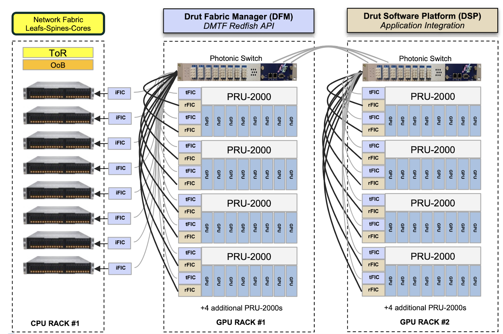
The smallest-sized DynamicXcelerator would use two racks of stacked PRU-2000s (see diagram). Further racks would be added to expand the system.
“The idea is that you can take a very large construct of things and create virtual PODs,” says Koss. “All of a sudden, you have flexible and fluid resources.”
Koss says a system can scale to 16,384 units by combining four clusters, each of 4,096 accelerators. “Each one can be designated as an ‘availability zone’, with users able to call resources in the different zones,” he says.
Customers might use such a configuration to segment users, run different AI models, or for security reasons. “It [a 16,384 unit system] would be huge and most likely something that only a service provider would do or maybe a government agency,” says Koss.
Capital and operation savings
Drut claims the architecture costs 30 per cent less than conventional systems, while operational cost-savings are 40 per cent.
The numbers need explaining, says Koss, given the many factors and choices possible.
The bill of materials of a 16, 32, 64 or 128-GPU design has a 10-30 per cent saving solely from the interconnect.
“The bigger the fabric, the better we scale in price as solutions using tiered leaf-spine-core packet switches involving Ethernet-Infiniband-PCIe are all built around the serdes of the switch chip in the box,” says Koss. “We have a direct-connect fabric with a very high radix, which allows us to build the fabric without stacked tiers like legacy point-to-point networks.”
There are also the power savings, as mentioned. Less power means less heat and hence less cooling.
“We can also change the physical wires in the network,” says Koss, something that can’t be done with leaf-spine-core networks, unless data centre staff change the cabling.
“By grouping resources around a workload, utilisation and performance are much better,” says Koss. “Apps run faster, infrastructure is grouped around workloads, giving users the power to do more with less.”
The system’s evolution is another consideration. A user can upgrade resources because of server disaggregation and the ability to add and remove resources from active machines.
“Imagine that you bought the DynamicXcelerator in 2024. Maybe it was a small sized, four-to-six rack system of GPUs, NVMe, etc,” says Koss. If, in mid-2026, Nvidia releases a new GPU, the user can take several PRU-2000s offline and replace the existing GPUs with the new ones.
“Also if you are an Nvidia shop but want to use the new Mi300 from AMD, no problem,” says Koss. “You can mix GPU vendors with the DynamicXcelerator.” This is different from today’s experience, where what is built is wasteful, expensive, complex, and certainly not climate-conscious, says Koss.
Plans for 2024
Drut has 31 employees, 27 of which are engineers. “We are going on a hiring binge and likely will at least double the company in 2024,” says Koss. “We are hiring in engineering, sales, marketing, and operations.”
Proof-of-concept DynamicXcelerator hardware will be available in the first half of 2024, with general availability then following.

Drut's agile optical fabric for the data centre
A US start-up has developed a photonic fabric for the data centre that pulls together the hardware needed for a computational task.
Drut Technologies offers management software and a custom line card, which, when coupled with the optical switch, grabs the hardware required for the workload.
“You can have a server with lots of resource machines: lots of graphic processing units (GPUs) and lots of memory,” says Bill Koss, CEO of Drut. “You create a machine, attach a workload to it and run it; forever, for a day, or 15 minutes.”
Drut first showcased its technology supporting the PCI Express (PCIe) bus over photonics at server specialist, SuperMicro’s exhibition stand, at the Supercomputing 22 show held last November in Dallas, Texas.
“This is a fully reconfigurable, direct-connect optical fabric for the data centre,” says Koss.
Drut says hyperscalers use between 40 and 60 per cent of the hardware in their data centres. With direct connectivity, resources can be used as needed and released, improving overall hardware utilisation.
Optical circuit switching
Drut’s system is a second recent example of a company using optics for the data centre to establish reconfigurable photonic paths between endpoints, referred to as optical circuit switching.
Google revealed in August 2022 that it had developed its own MEMS-based optical switch design, which the hyperscaler has used for several years in its data centres.
The optical circuit switches are used instead of the highest tier of Ethernet switches – the spine layer – in Google’s data centres.
Using optical circuit switching reduces networking costs by 30 per cent and power consumption by over 40 per cent. The optical switch layer also enables more efficient and less disruptive upgrading of the server endpoints.
Koss says the difference between its design and Google’s is scale: “Ours is more granular.”
Drut says its solution will enable racks of optically-attached machines, but unlike Google, the optical switching is much closer to the end equipment. Indeed, it is a second fabric independent of the data centre’s tiered Ethernet switches.

Product architecture
The main three elements of Drut’s technology are an FPGA-based line card, the fabric-manager software and a third-party optical switch.
Drut’s line card, the iFIC 1000, has an FPGA and four 100-gigabit transceivers. “That is as much as we can fit on,” says Koss.

The company uses its own transport protocol that runs over the fabric, an ‘out-of-band’ network design.
“You can dynamically attach and detach, and the machine doesn’t go into crazy land,” says Koss.
The fabric manager knows all the ports of the switch and the endpoints and sets up the desired system configurations.
With the fabric management software and the FPGA, the system can configure banks of graphic processing units (GPUs).
Drut has also demonstrated linking memory over its photonic fabric, although this is in development and still unavailable as a product.
Drut says a primary challenge was developing the FPGA that takes the out-of-band signalling off the main bus and supports it over the optical fabric.
A photonic fabric design promises to change the nature of a server. A user will request CPUs, accelerators such as GPUs and FPGAs, and memory, as needed, for each workload.
The merits of using an optical switch include its support for multiple ports, i.e. the switch’s large radix, and its being interface-speed agnostic.
The photonic switch also has a lower latency than switch ICs and simplifies cabling. “It is all single-mode fibre pluggable optics,” says Koss.

Status
Drut is developing a second line card which will use a larger FPGA. Each card generation will expand the number of optical ports to scale the endpoints supported.
The company is also working with a co-packaged optics player on a design for a hyperscaler.
“We use pluggable optics today because co-packaged optics isn’t available,” says Koss.
The advantage of co-packaged optics is that it will increase the port density on each line card and hence the overall scaling.
Koss says that Drut already has two customers: an enterprise and a cloud provider.
Drut, which means ‘high tempo’ in Sanskrit, has so far secured two rounds of funding.
“We did a good-sized seed round in June 2021 and closed a bigger seed extension last September; not an easy task in 2022,” says Koss. “We added Boston Seed Capital and another firm as new investors as well.”
The company has sufficient funding till 2024 and is talking to new investors for a Series A funding round.

PCI-SIG releases the next PCI Express bus specification

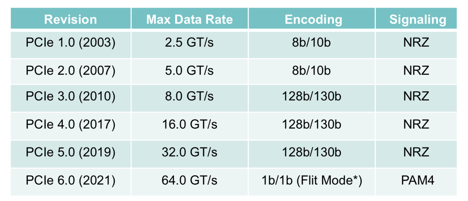
The Peripheral Component Interconnect Express (PCIe) 6.0 specification doubles the data rate to deliver 64 giga-transfers-per-second (GT/s) per lane.
For a 16-lane configuration, the resulting bidirectional data transfer capacity is 256 gigabytes-per-second (GBps).
“We’ve doubled the I/O bandwidth in two and a half years, and the average pace is now under three years,” says Al Yanes, President of the Peripheral Component Interconnect – Special Interest Group (PCI-SIG).
The significance of the specification’s release is that PCI-SIG members can now plan their products.
Users of FPGA-based accelerators, for example, will know that in 12-18 months there will be motherboards running at such rates, says Yanes
Applications
The PCIe bus is used widely for such applications as storage, processors, artificial intelligence (AI), the Internet of Things (IoT), mobile, and automotive.
In servers, PCIe has been adopted for storage and by general-purpose processors and specialist devices such as FPGAs, graphics processor units (GPUs) and AI hardware.
The CXL standard enables server disaggregation by interconnecting processors, accelerator devices, memory, and switching, with the protocol sitting on top of the PCIe physical layer. The NVM Express (NVMe) storage standard similarly uses PCIe.
“If you are on those platforms, you know you have a healthy roadmap; this technology has legs,” says Yanes.
A focus area for PCI-SIG is automotive which accounts for the recent membership growth; the organisation now has 900 members. PCI-SIG has also created a new workgroup addressing automotive.
Yanes attributes the automotive industry’s interest in PCIe due to the need for bandwidth and real-time analysis within cars. Advanced driver assistance systems, for example, use a variety of sensors and technologies such as AI.
PCIe 6.0
The PCIe bus uses a dual simplex scheme – serial transmissions in both directions – referred to as a lane. The bus can be configured in several lane configurations: x1, x2, x4, x8, x12, x16 and x32, although x2, x12 and x32 are rarely used.
PCIe 6.0’s 64GT/s per lane is double that of PCIe 5.0 that is already emerging in ICs and products.
IBM’s latest 7nm POWER10 16-core processor, for example, uses the PCIe 5.0 bus as part of its I/O, while the latest data processing units (DPUs) from Marvell (Octeon 10) and Nvidia (BlueField 3) also support PCIe 5.0.
To achieve the 64GT/s transfer rates, the PCIe bus has adopted 4-level pulse amplitude modulation (PAM-4) signalling. This requires forward error correction (FEC) to offset the bit error rates of PAM-4 while minimising the impact on latency. And low latency is key given the PCIe PHY layer is used by such protocols as CXL that carry coherency and memory traffic. (see IEEE Micro article.)
The latest specification also adopts flow control unit (FLIT) encoding. Here, fixed 256-byte packets are sent: 236 bytes of data and 20 bytes of cyclic redundancy check (CRC).
Using fixed-length packets simplifies the encoding, says Yanes. Since the PCIe 3.0 specification, 128b/130b encoding has been used for clock recovery and the aligning of data. Now with the fixed-sized packet of FLIT, no encoding bits are needed. “They know where the data starts and where it ends,” says Yanes.
Silicon designed for PCIe 6.0 will also be able to use FLITs with earlier standard PCIe transfer speeds.
Yanes says power-saving modes have been added with the release. Both ends of a link can agree to make lanes inactive when they are not being used.
Status and developments
IP blocks for PCIe 6.0 already exist while demonstrations and technology validations will occur this year. First products using PCIe 6.0 will appear in 2023.
Yanes expects PCIe 6.0 to be used first in servers with accelerators used for AI and machine learning, and also where 800 Gigabit Ethernet will be needed.
PCI-SIG is also working to develop new cabling for PCIe 5.0 and PCIe 6.0 for sectors such as automotive. This will aid the technology’s adoption, he says
Meanwhile, work has begun on PCIe 7.0.
“I would be ecstatic if we can double the data rate to 128GT/s in two and a half years,” says Yanes. “We will be investigating that in the next couple of months.”
One challenge with the PCIe standard is that it borrows the underlying technology from telecom and datacom. But the transfer rates it uses are higher than the equivalent rates used in telecom and datacom.
So, while PCI 6.0 has adopted 64GT/s, the equivalent rate used in telecom is 56Gbps only. The same will apply if PCI-SIG chooses 128GT/s as the next data rate given that telecom uses 112Gbps.
Yanes notes, however, that telecom requires much greater reaches whereas PCIe runs on motherboards, albeit ones using advanced printed circuit board (PCB) materials.

Xilinx’s Versal Premium ready for the 800-gigabit era
When Xilinx was created in 1984, the founders banked on programmable logic becoming ever more attractive due to Moore’s law.
Making logic programmable requires extra transistors so Xilinx needed them to become cheaper and more plentiful, something Moore’s law has delivered, like clockwork, over decades.
Since then, Xilinx’s field-programmable gate array (FPGA) devices have advanced considerably.
Indeed, Xilinx’s latest programmable logic family, the Versal Premium, is no longer referred to as an FPGA but as an adaptive compute accelerator platform (ACAP).
The Versal Premium series of chips, to be implemented using TSMC’s 7nm CMOS process, was unveiled for the OFC 2020 show. The Premium series will have seven chips with the largest, the VP1802, having 50 billion transistors.
First devices will ship in the second half of 2021.
ACAP series
Xilinx unveiled its adaptive compute acceleration platform in 2018.

Kirk Saban
“It is a complete rearchitecting of our device technology,” says Kirk Saban, vice president product and platform marketing at Xilinx. “It is heterogenous by nature and has multiple types of processing engines.”
“Versal Premium is evolutionary compared with previous FPGAs that have hardened blocks for certain functions,” says Bob Wheeler, principal analyst at The Linley Group. “It is another step along a continuum, not really new.”
Six ACAP families are planned for Versal: three tailored for artificial intelligence (AI) - the AI RF, AI Core and AI Edge - and the others being the Prime, Premium and HBM (high bandwidth memory).
Only Versal AI series will have AI engines: very-long-instructing-word (VLIW) processor cores that can also be used for computational-intensive tasks such as digital signal processing.
Premium is the third Versal family to be unveiled, joining the AI Core and Prime series.
Versal Prime is Xilinx’s broadest series in the portfolio, featuring a range of device sizes and capabilities. The Prime series is suited to such applications as storage acceleration in the data centre; wired networking such as 5G back-, mid- and front-haul, and passive optical networking; and industrial applications such as machine vision.
Networking needs
Versal Premium has been developed with core networking and data centre acceleration applications in mind.
“The top-end SKU handles high-end networking applications such as optical transport and data centre interconnect as well as the most demanding signal-processing applications such as radar systems,” says Wheeler.
Xilinx defines core networking as the infrastructure beyond the radio access network. “All the wireline infrastructure is what we consider to be the core of the network,” says Saban. “Access, metro, and core networks, all together.”
When Xilinx’s designers sat down to consider the networking needs for the coming six years, they anticipated a huge capacity hike in the core network. Device numbers are set to grow tenfold with each device generating ten times more traffic.
“The bandwidth going through the wired network globally needs to grow at 50 per cent on a compound annual basis to keep pace with the number of devices being connected and the data coming through them,” says Saban.
Versal Premium will deliver three times the bandwidth and nearly twice the logic capacity of the 16nm Virtex UltraScale+ VU13P FPGA, the largest device used currently for networking and data centre applications.
“Shifts are happening that the Virtex FPGAs are not going to be able to handle,” says Saban. “The move to 400 gigabit and then 800 gigabit on the mid-term horizon, the Virtex products can’t handle that kind of throughput.”
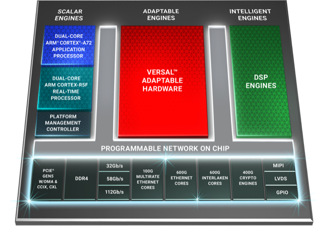
Versal Premium architecture. Source: Xilinx
Premium architecture
The Premium devices feature ARM-based scalar processors such as the dual-core Cortex-A72 application processor and the dual-core Cortex-R5F real-time processor.
The application processor is used for general-purpose processing and control. The real-time processor is used for applications that require deterministic processing. Such a processor is key for safety-certified applications.
Also included is a platform management controller that oversees the device. A user can configure many of the ACAP settings using a standard tool flow but the controller’s operation is effectively transparent to the user, says Saban.
The Premium features several types of on-chip memory that Saban likens to levels of cache memory used by high-performance processors. ”We have look-up-table RAM, Block RAM and Ultra RAM and we can offload to [external] DDR4 [RAM],” he says. “The memory hierarchy can be configured to match the algorithm you are building.”
The various on-chip functional blocks are linked via a programmable network-on-a-chip. Having the network-on-a-chip frees up programmable logic resources that would otherwise be required to connect the design’s functional blocks.
“Equipment manufacturers need to deliver on this core network growth but they also need to do it securely,” says Saban. “With everything shifting to the cloud, there are huge concerns about data privacy; in many instances, security is just as important as performance for the operators.”
To this aim, the Premium’s on-chip peripherals include 400-gigabit crypto-engines that support the AES-GCM-256 and -128, MACsec, and IPSec encryption standards.
“The crypto blocks are unique and save a lot of look-up tables and power compared with implementing these in programmable logic,” says Linley’s Wheeler.
Other on-chip features include up to 5 terabits of Ethernet throughput supporting rates from 10 to 400 Gigabit Ethernet. The devices have multiple 600-gigabit Ethernet MAC cores and support such protocols as FlexE, Flex-O, Ethernet CPRI (eCPRI), Fibre Channel over Ethernet (FCoE), and OTN.
The Premium family delivers up to 1.8 terabits of Interlaken, from 10-gigabit to 600-gigabit interfaces. Interlaken enables chip-to-chip and chip-to-backplane communications.
There are also 112-gigabit 4-level pulse-amplitude modulation (PAM-4) serialisers/ deserialisers (serdes). The VP1802 will have 28, 32-gigabit serdes and either 140, 58-gigabit or 70, 112-gigabit serdes. The electrical transceivers can drive 10m of copper cable, says Saban.
PCI Express Generation 5.0, enabling direct memory access and cache-coherent interconnect, is also supported on-chip. “We can connect to server CPUs and be an extension of their memory map,” says Saban.
Xilinx claims 22 UltraScale+ FPGAs would be needed to implement all the logic and peripherals of the Versal Premium VP1802.
System design
Wireline vendors want to double the performance with each generation of equipment while keeping platform size and power consumption constant.
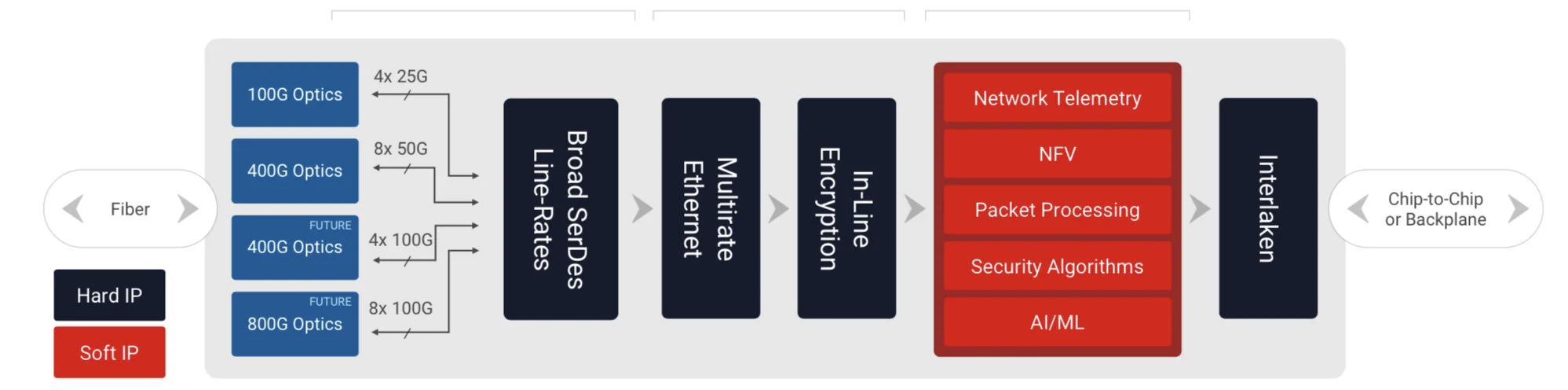
Xilinx has a diagram (shown) of a generic telecom line-card design using the Versal Premium. “Vendors have different variants but at a high-level, they all look like this,” says Saban.
Generic telecom line card using the Versal Premium. Source: Xilinx
Line-card data arrives via optical modules. At present 100-gigabit is mainstream with 400-gigabit coming soon, and eventually 800-gigabit interfaces. The data is fed to the Premium’s hardened logic blocks: the Ethernet and encryption blocks.
The adaptive logic (in red) is what companies use to implement their unique designs such as executing virtualised network functions (NFV) or for packet processing.
“We are seeing the need to infuse artificial intelligence and machine learning into these applications in some capacity,” says Saban. Premium devices have no AI VLIW cores but have sufficient resources for some level of artificial intelligence/ machine learning capability.
Interlaken then sends the data to a host chip or across the backplane to another line card.
Software tools
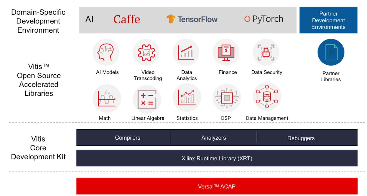
Xilinx stresses the company is no longer a chip provider but a platform provider. This is reflected in the software tools it provides to accompany its silicon.
Vitis software tool. Source: Xilinx
Versal ACAPs come with advanced toolkit libraries so engineers can program the chip with no knowledge of the underlying hardware.
Xilinx is continuing to provide its Vivado toolset that supports register-transfer level (RTL), a design abstraction used by hardware engineers for their circuit designs. “The traditional RTL toolchain is not going away and will continue to evolve,” says Saban.
But coders developing data centre applications with no knowledge of RTL or programmable logic can now use Xilinx’s Vitis toolset that was launched in 2019.
“It is critical to enable software developers and data scientists doing machine learning a way to interface to our [ACAP] products,” says Saban.
Vitis supports programming languages such as C, C++ and Python as well as higher-level machine-learning frameworks such as TensorFlow and Caffe.
Xilinx also has a library of functions for tasks such as data analytics and genomics. Such applications can be switched in and out since they are executed using adaptive hardware.
The Premium software tools will be available in the fourth quarter of the year.
Lifespan
A programmable logic family’s lifespan is five or six years; the Virtex UltraScale family was launched in 2015.
“We added a few kickers [to the Virtex family] such as high bandwidth memory and 58-gigabit serdes,” says Saban. “And we will likely do the same with Versal, add some integrated block in a derivative product.”
Xilinx’s chip designers will likely now be already working on an ACAP architecture for 2026 supporting 1.6-terabit speeds and to be implemented using a 5nm CMOS process.
“If we are to deliver twice the bandwidth at half the power, it is not enough to lean on CMOS process technology,” says Saban. “We will need to look at new chip architectures to solve the problems.”
This is challenging. “It gets harder, it gets more expensive and there are less and fewer companies that can afford it,” says Saban.

Will white boxes predominate in telecom networks?
Will future operator networks be built using software, servers and white boxes or will traditional systems vendors with years of network integration and differentiation expertise continue to be needed?
AT&T’s announcement that it will deploy 60,000 white boxes as part of its rollout of 5G in the U.S. is a clear move to break away from the operator pack.
The service provider has long championed network transformation, moving from proprietary hardware and software to a software-controlled network based on virtual network functions running on servers and software-defined networking (SDN) for the control switches and routers.
 Glenn WellbrockNow, AT&T is going a stage further by embracing open hardware platforms - white boxes - to replace traditional telecom hardware used for data-path tasks that are beyond the capabilities of software on servers.
For the 5G deployment, AT&T will, over several years, replace traditional routers at cell and tower sites with white boxes, built using open standards and merchant silicon.
“White box represents a radical realignment of the traditional service provider model,” says Andre Fuetsch, chief technology officer and president, AT&T Labs. “We’re no longer constrained by the capabilities of proprietary silicon and feature roadmaps of traditional vendors.”
But other operators have reservations about white boxes. “We are all for open source and open [platforms],” says Glenn Wellbrock, director, optical transport network - architecture, design and planning at Verizon. “But it can’t just be open, it has to be open and standardised.”
Wellbrock also highlights the challenge of managing networks built using white boxes from multiple vendors. Who will be responsible for their integration or if a fault occurs? These are concerns SK Telecom has expressed regarding the virtualisation of the radio access network (RAN), as reported by Light Reading.
“These are the things we need to resolve in order to make this valuable to the industry,” says Wellbrock. “And if we don’t, why are we spending so much time and effort on this?”
Gilles Garcia, communications business lead director at programmable device company, Xilinx, says the systems vendors and operators he talks to still seek functionalities that today’s white boxes cannot deliver. “That’s because there are no off-the-shelf chips doing it all,” says Garcia.
We’re no longer constrained by the capabilities of proprietary silicon and feature roadmaps of traditional vendors
White boxes
AT&T defines a white box as an open hardware platform that is not made by an original equipment manufacturer (OEM).
A white box is a sparse design, built using commercial off-the-shelf hardware and merchant silicon, typically a fast router or switch chip, on which runs an operating system. The platform usually takes the form of a pizza box which can be stacked for scaling, while application programming interfaces (APIs) are used for software to control and manage the platform.
As AT&T’s Fuetsch explains, white boxes deliver several advantages. By using open hardware specifications for white boxes, they can be made by a wider community of manufacturers, shortening hardware design cycles. And using open-source software to run on such platforms ensures rapid software upgrades.
Disaggregation can also be part of an open hardware design. Here, different elements are combined to build the system. The elements may come from a single vendor such that the platform allows the operator to mix and match the functions needed. But the full potential of disaggregation comes from an open system that can be built using elements from different vendors. This promises cost reductions but requires integration, and operators do not want the responsibility and cost of both integrating the elements to build an open system and integrating the many systems from various vendors.
Meanwhile, in AT&T’s case, it plans to orchestrate its white boxes using the Open Networking Automation Platform (ONAP) - the ‘operating system’ for its entire network made up of millions of lines of code.
ONAP is an open software initiative, managed by The Linux Foundation, that was created by merging a large portion of AT&T’s original ECOMP software developed to power its software-defined network and the OPEN-Orchestrator (OPEN-O) project, set up by several companies including China Mobile and China Telecom.
AT&T has also launched several initiatives to spur white-box adoption. One is an open operating system for white boxes, known as the dedicated network operator system (dNOS). This too will be passed to The Linux Foundation.
The operator is also a key driver of the open-based reconfigurable optical add/ drop multiplexer multi-source agreement, the OpenROADM MSA. Recently, the operator announced it will roll out OpenROADM hardware across its network. AT&T has also unveiled the Akraino open source project, again under the auspices of the Linux Foundation, to develop edge computing-based infrastructure.
At the recent OFC show, AT&T said it would limit its white box deployments in 2018 as issues are still to be resolved but that come 2019, white boxes will form its main platform deployments.
Xilinx highlights how certain data intensive tasks - in-line security, performed on a per-flow basis, routing exceptions, telemetry data, and deep packet inspection - are beyond the capabilities of white boxes. “White boxes will have their place in the network but there will be a requirement, somewhere else in the network for something else, to do what the white boxes are missing,” says Garcia.
Transport has been so bare-bones for so long, there isn’t room to get that kind of cost reduction
AT&T also said at OFC that it expects considerable capital expenditure cost savings - as much as a halving - using white boxes and talked about adopting in future reverse auctioning each quarter to buy its equipment.
Niall Robinson, vice president, global business development at ADVA Optical Networking, questions where such cost savings will come from: “Transport has been so bare-bones for so long, there isn’t room to get that kind of cost reduction. He also says that there are markets that already use reverse auctioning but typically it is for items such as components. “For a carrier the size of AT&T to be talking about that, that is a big shift,” says Robinson.
Layer optimisation
Verizon’s Wellbrock first aired reservations about open hardware at Lightwave’s Open Optical Conference last November.
In his talk, Wellbrock detailed the complexity of Verizon’s wide area network (WAN) that encompasses several network layers. At layer-0 are the optical line systems - terminal and transmission equipment - onto which the various layers are added: layer-1 Optical Transport Network (OTN), layer-2 Ethernet and layer-2.5 Multiprotocol Label Switching (MPLS). According to Verizon, the WAN takes years to design and a decade to fully exploit the fibre.
“You get a significant saving - total cost of ownership - from combining the layers,” says Wellbrock. “By collapsing those functions into one platform, there is a very real saving.” But there is a tradeoff: encapsulating the various layers’ functions into one box makes it more complex.
“The way to get round that complexity is going to a Cisco, a Ciena, or a Fujitsu and saying: ‘Please help us with this problem’,” says Wellbrock. “We will buy all these individual piece-parts from you but you have got to help us build this very complex, dynamic network and make it work for a decade.”
Next-generation metro
Verizon has over 4,000 nodes in its network, each one deploying at least one ROADM - a Coriant 7100 packet optical transport system or a Fujitsu Flashwave 9500. Certain nodes employ more than one ROADM; once one is filled, a second is added.
“Verizon was the first to take advantage of ROADMs and we have grown that network to a very large scale,” says Wellbrock.
The operator is now upgrading the nodes using more sophiticated ROADMs, as part of its next-generation metro. Now each node will need only one ROADM that can be scaled. In 2017, Verizon started to ramp and upgraded several hundred ROADM nodes and this year it says it will hit its stride before completing the upgrades in 2019.
“We need a lot of automation and software control to hide the complexity of what we have built,” says Wellbrock. This is part of Verizon’s own network transformation project. Instead of engineers and operational groups in charge of particular network layers and overseeing pockets of the network - each pocket being a ‘domain’, Verizon is moving to a system where all the networks layers, including ROADMs, are managed and orchestrated using a single system.
The resulting software-defined network comprises a ‘domain controller’ that handles the lower layers within a domain and an automation system that co-ordinates between domains.
“Going forward, all of the network will be dynamic and in order to take advantage of that, we have to have analytics and automation,” says Wellbrock.
In this new world, there are lots of right answers and you have to figure what the best one is
Open design is an important element here, he says, but the bigger return comes from analytics and automation of the layers and from the equipment.
This is why Wellbrock questions what white boxes will bring: “What are we getting that is brand new? What are we doing that we can’t do today?”
He points out that the building blocks for ROADMs - the wavelength-selective switches and multicast switches - originate from the same sub-system vendors, such that the cost points are the same whether a white box or a system vendor’s platform is used. And using white boxes does nothing to make the growing network complexity go away, he says.
“Mixing your suppliers may avoid vendor lock-in,” says Wellbrock. “But what we are saying is vendor lock-in is not as serious as managing the complexity of these intelligent networks.”
Wellbrock admits that network transformation with its use of analytics and orchestration poses new challenges. “I loved the old world - it was physics and therefore there was a wrong and a right answer; hardware, physics and fibre and you can work towards the right answer,” he says. “In this new world, there are lots of right answers and you have to figure what the best one is.”
Evolution
If white boxes can’t perform all the data-intensive tasks, then they will have to be performed elsewhere. This could take the form of accelerator cards for servers using devices such as Xilinx’s FPGAs.
Adding such functionality to the white box, however, is not straightforward. “This is the dichotomy the white box designers are struggling to address,” says Garcia. A white box is light and simple so adding extra functionality requires customisation of its operating system to run these application. And this runs counter to the white box concept, he says.
We will see more and more functionalities that were not planned for the white box that customers will realise are mandatory to have
But this is just what he is seeing from traditional systems vendors developing designs that are bringing differentiation to their platforms to counter the white-box trend.
One recent example that fits this description is Ciena’s two-rack-unit 8180 coherent network platform. The 8180 has a 6.4-terabit packet fabric, supports 100-gigabit and 400-gigabit client-side interfaces and can be used solely as a switch or, more typically, as a transport platform with client-side and coherent line-side interfaces.
The 8180 is not a white box but has a suite of open APIs and has a higher specification than the Voyager and Cassini white-box platforms developed by the Telecom Infra Project.
“We are going through a set of white-box evolutions,” says Garcia. “We will see more and more functionalities that were not planned for the white box that customers will realise are mandatory to have.”
Whether FPGAs will find their way into white boxes, Garcia will not say. What he will say is that Xilinx is engaged with some of these players to have a good view as to what is required and by when.
It appears inevitable that white boxes will become more capable, to handle more and more of the data-plane tasks, and as a response to the competition from traditional system vendors with their more sophisticated designs.
AT&T’s white-box vision is clear. What is less certain is whether the rest of the operator pack will move to close the gap.
FPGAs with 56-gigabit transceivers set for 2017
The company demonstrated a 56-gigabit transceiver using 4-level pulse-amplitude modulation (PAM-4) at the recent OFC show. The 56-gigabit transceiver, also referred to as a serialiser-deserialiser (serdes), was shown successfully working over backplane specified for 25-gigabit signalling only.
 Gilles GarciaXilinx's 56-gigabit serdes is implemented using a 16nm CMOS process node but the first FPGAs featuring the design will be made using a 7nm process. Gilles Garcia says the choice of 7nm CMOS is solely a business decision and not a technical one.
”Optical module [makers] will take another year to make something decent using PAM-4," says Garcia, Xilinx's director marketing and business development, wired communications. "Our 7nm FPGAs will follow very soon afterwards.”
The company is still to detail its next-generation FPGA family but says that it will include an FPGA capable of supporting 1.6 terabit of Optical Transport Network (OTN) using 56-gigabit serdes only. At first glance that implies at least 28 PAM-4 transceivers on a chip but OTN is a complex design that is logic not I/O limited suggesting that the FPGA will feature more than 28, 56-gigabit serdes.
Applications
Xilinx’s Virtex UltraScale and its latest UltraScale+ FPGA families feature 16-gigabit and 25-gigabit transceivers. Managing power consumption and maximising reach of the high-speed serdes are key challenges for its design engineers. Xilinx says it has 150 engineers for serdes design.
“Power is always a key challenge because as soon as you talk about 400-gigabit to 1-terabit per line card, you need to be cautious about the power your serdes will use,” says Garcia. He says the serdes need to adapt to the quality of the traces for backplane applications. Customers want serdes that will support 25 gigabit on existing 10-gigabit backplane equipment.
Xilinx describes its Virtex UltraScale as a 400-gigabit capable single-chip system supporting up to 104 serdes: 52 at 16 gigabit and 52 at 25 gigabit.
The UltraScale+ is rated as a 500-gigabit to 600-gigabit capable system, depending on the application. For example, the FPGA could support three, 200-gigabit OTN wavelengths, says Garcia.
Xilinx says the UltraScale+ reduces power consumption by 35% to 50% compared to the same designs implemented on the UltrasScale. The Virtex UltraScale+ devices also feature dedicated hardware to implement RS-FEC, freeing up programmable logic for other uses. RS-FEC is used with multi-mode fibre or copper interconnects for error correction, says Xilinx. Six UltraScale+ FPGAs are available and the VU13P, not yet out, will feature up to 128 serdes, each capable of up to 32 gigabit.
We don’t need retimers so customers can connect directly to the backplane at 25 gigabit, thereby saving space, power and cost
The UltraScale and UltraScale+ FPGAs are being used in several telecom and datacom applications.
For telecom, 500-gigabit and 1-terabit OTN designs are an important market for the UltraScale FPGAs. Another use for the FPGA serdes is for backplane applications. “We don’t need retimers so customers can connect directly to the backplane at 25 gigabit, thereby saving space, power and cost,” says Garcia. Such backplane uses include OTN platforms and data centre interconnect systems.
The FPGA family’s 16-gigabit serdes are also being used in 10-gigabit PON and NG-PON2 systems. “When you have an 8-port or 16-port system, you need to have a dense serdes capability to drive the [PON optical line terminal’s] uplink,” says Garcia.
For data centre applications, the FPGAs are being employed in disaggregated storage systems that involved pooled storage devices. The result is many 16-gigabit and 25-gigabit streams accessing the storage while the links to the data centre and its servers are served using 100-gigabit links. The FPGA serdes are used to translate between the two domains (see diagram).
 Source: Xilinx
For its next-generation 7nm FPGAs with 56-gigabit transceivers, Xilinx is already seeing demand for several applications.
Data centre uses include server-to-top-of-rack links as the large Internet providers look move from 25 gigabit to 50- and 100-gigabit links. Another application is to connect adjacent buildings that make up a mega data centre which can involve hundreds of 100-gigabit links. A third application is meeting the growing demands of disaggregated storage.
For telecom, the interest is being able to connect directly to new optical modules over 50-gigabit lanes, without the need for gearbox ICs.
Optical FPGAs
Altera, now part of Intel, developed an optical FPGA demonstrator that used co-packaged VCSELs for off-chip optical links. Since then Altera announced its Stratix 10 FPGAs that include connectivity tiles - transceiver logic co-packaged and linked with the FPGA using interposer technology.
Xilinx says it has studied the issue of optical I/O and that there is no technical reason why it can’t be done. But the issue is a business one when integrating optics in an FPGA, he says: “Who is responsible for the yield? For the support?”
Garcia admits Xilinx could develop its own I/O designs using silicon photonics and then it would be responsible for the logic and the optics. “But this is not where we are seeing the business growing,” he says.
OpenCL and the reconfigurable data centre
Part 3: General purpose data centres
Xilinx's adoption of the Open Computing Language (OpenCL) as part of its SDAccel development tool is important, not just for FPGAs but also for the computational capabilities of the data centre.
The FPGA vendor is promoting its chips as server co-processors to tackle complex processing tasks such as image searches, encryption, and custom computation.
Search-engine specialists such as Baidu and Microsoft have seen a greater amount of traffic for image and video searches in the last two years, says Loring Wirbel, senior analyst at market research firm, The Linley Group: "All of a sudden they are seeing that these accelerator cards as being necessary for general-purpose data centres."
Xilinx and Altera have been way ahead of the niche FPGA vendors, indeed ahead of a lot of the network processor and graphics processor (GPU) vendors, in recognising the importance of OpenCL
OpenCL was developed by Apple and is being promoted by the Khronos Group, an industry consortium set up to promote the integration of general purpose microprocessors, graphics processors, and digital signal processing blocks. And it is the FPGA vendors that are playing a pivotal role in OpenCL's adoption.
"Xilinx and Altera have been way ahead of the niche FPGA vendors, indeed ahead of a lot of the network processor and graphics processor (GPU) vendors, in recognising the importance of OpenCL," says Wirbel.
Altera announced the first compiler kit for OpenCL in 2013. "The significant thing Altera did was develop 'channels' for accelerator 'kernels'. Using the channels, kernels - the tasks to be accelerated in hardware - communicate with each other without needing the host processor. "It offers an efficient way for multiple co-processors to talk to each other," says Wirbel. The OpenCL community have since standardised elements of Altera's channels, now referred to as pipes.
"What Xilinx has brought with SDAccel is probably more significant in that it changes the design methodology for bringing together CPUs and GPUs with FPGAs," says Wirbel. Xilinx's approach may be specific to its FPGAs but Wirbel expects other firms to adopt a similar design approach. "Xilinx has created a new way to look at design that will ease the use of parallelism in general, and OpenCL," says Wirbel. (see SDAccel design approach, below.)
"Altera and Xilinx should be saluted in that they have encouraged people to start looking at OpenCL as a move beyond C for programming everything," says Wirbel. This broadening includes programming multi-core x86 and ARM processors, where a good parallel language is desirable. "You get better performance moving from C to C++, but OpenCL is a big jump," he says.
The future says that every data centre is going to become an algorithmically-rich one that can suddenly be reallocated to do other tasks
Wirbel does not have hard figures as to how many of a data centre's servers will have accelerator cards but he believes that every data centre is going to have specialised acceleration for tasks such as imaging and encryption as a regular feature within the next year or two. His educated guess is that it will be one accelerator card per eight host CPUs and possibly one in four.
Longer terms, such acceleration will change the computational nature of the data centre. "The future says that every data centre is going to become an algorithmically-rich one that can suddenly be reallocated to do other tasks," he says. It could mean that institutions such as national research labs that tackle huge-scale simulation work may no longer require specialist supercomputer resources.
"That is a little bit exaggerated because what will really happen is you will have to have whole clusters of data centres around the country allocated to ad-hoc virtual multiprocessing on very difficult problems," says Wirbel. "But the very notion that there needs to be assigned computers in data centres to one set of problems will be a thing of the past."
How does that relate to Xilinx's SDAccel and OpenCL?
"Some of this will happen because of tools like OpenCL as the language and tools like SDAccel for improving FPGAs," says Wirbel.
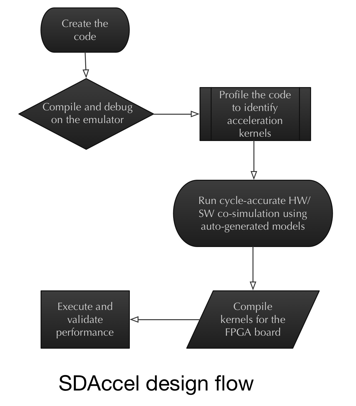
The SDAccel design approach
Xilinx has adopted the concept of co-simulation at an early stage of an FPGA-based co-processor design, alongside a server's x86 processor.
Wirbel says that despite all the talk about co-simulation over the last decade, little has been done in practice. With co-simulation, an x86 processor or a graphics processor is simulated with a designer's IP logic that makes up an ASIC or an FPGA design.
Making FPGAs with very tightly-packed processors and with a very low power dissipation is critical; it is a big deal
"What Xilinx did is they said: the biggest problem is designers having to redo an FPGA, even placing and routing elements and going back to using back-end EDA [electronic design automation] tools," says Wirbel. "Maybe the best way of doing this is recognising we have to do some early co-simulation on a target x86 CPU board."
This is where OpenCL plays a role.
"The power of OpenCL is that it lets you define an acceleration task as a kernel," says Wirbel. It is these acceleration kernels that are sent to the hardware emulator with the x86 on board. The kernels can then be viewed in the co-simulation environment working alongside the x86 such that any problems encountered can be tackled, and the two optimised. "Then, and only then, do you send it to a compiler for a particular FPGA architecture."
The challenge for Xilinx is keeping a lid on the FPGA accelerator card's power consumption given the huge number of servers in a data centre.
"The large internet players have got to be able to add these new features for almost zero extra power," says Wirbel. "Making FPGAs with very tightly-packed processors and with a very low power dissipation is critical; it is a big deal."
For Part 1, click here
For Part 2, click here
What role FPGA server co-processors for virtual routing?
IP routing specialists have announced first virtual edge router products that run on servers. These include Alcatel-Lucent with its Virtualized Service Router and Juniper with its vMX. Gazettabyte asked Alcatel-Lucent's Steve Vogelsang about the impact FPGA accelerator cards could have on IP routing.

Steve Vogelsang, IP routing and transport CTO, Alcatel-Lucent
The co-processor cards in servers could become interesting for software-defined networking (SDN) and network function virtualisation (NFV).
The main challenge is that we require that our virtualised network functions (vNFs) and SDN data plane can run on any cloud infrastructure; we can’t assume that any specific accelerator card is installed. That makes it a challenge.
I can imagine, over time, that DPDK, the set of libraries and drivers for packet processing, and other open source libraries will support co-processors, making it easier to exploit by an SDN data plane or vNF.
For now we’re not too worried about pushing the limits of performance because the advantage of NFV is the operational simplicity. However, when we have vNFs running at significant scale, we will likely evaluate co-processor options to improve performance. This is similar to what Microsoft and others are doing with search algorithms and other applications.
Note that there are alternative co-processors that are more focussed on networking acceleration. An example is Netronome which is a purpose-built network co-processor for the x86 architecture. Not sure how it compares to Xilinx for networking functionality, but it may outperform FPGAs and be a better option if networking is the focus.
Some servers are also built to enable workload-specific processing architectures. Some of these are specialised on a single processor architecture while others such as HP's Moonshot allow installation of various processors including FPGAs.
When we have vNFs running at significant scale, we will likely evaluate co-processor options to improve performance
I don’t expect FPGA accelerator cards will have much impact on network processors (NPUs). We or any other vendor could build an NPU using a Xilinx or another FPGA. But we get much more performance by building our own NPU because we control how we use the chip area.
When designing an FPGA, Xilinx and other FPGA vendors have to decide how to allocate chip space to I/O, processing cores, programmable logic, memory, and other functional blocks. The resulting structure can deliver excellent performance for a variety of applications, but we can still deliver considerably more performance by designing our own chips allocating the chip space needed to the required functions.
I have experience with my previous company which built multiple generations of NPUs using FPGAs, but they could not come close to the capabilities of our FP3 chipset.
For Part 1, click here
For Part 3, click here
Cortina unveils multi-channel dispersion compensation chip
Cortina Systems has announced its latest electronic dispersion compensation (EDC) chip. The CS4342 is a compact device that supports eight duplex 10 Gigabit-per-second (Gbps) links.

"Some customers are doing 2,000 signals at 10 Gig across the backplane"
Scott Feller, Cortina
The chip is suited for use with optical modules and on line cards to counter the effect of transmission distortion where a bit's energy leaks into one or more adjacent bits, known as inter-symbol interference (ISI).
The Cortina device can be used for 10, 40 and 100Gbps line card and backplane designs and supports copper cable and optical fibre standards such as the multimode 10GBASE‐LRM and the 80km 10GBASE‐ZR interface.
Significance
Routeing high-speed signals from an ASIC to the various high-speed interfaces - 10Gbps and greater - is becoming harder as more interfaces are crammed onto a card.
"Boards are getting denser: from 48 ports to 96," says Scott Feller, director of the EDC product line at Cortina Systems. The issue with an ASIC on the board is that the distance it can span to the modules is only about 6-8 inches (~15-20cm). Placing the PHY chip on the board relaxes this constraint.
 The use of the octal EDC chip between a line card IC and SFP+ optical transceivers. Source: Cortina Systems
Vendors also gain greater flexibility in terms of the interfaces they can support. "These types of PHYs allow them [designers] to avoid having to make hard decisions," says Feller. "They put the PHY in front of the optical connector and they almost get every single optical format on the market."
The platforms using such EDC PHYs include data centre switches and telecom platforms such as packet optical transport systems (P-OTS). Data centre switches typically support Direct Attach Copper cable - a market area that has been growing significantly, says Cortina - and short-reach optical interfaces. For P-OTS the interfaces include the 10GBASE-ZR where EDC is a necessity.
The device is also being used for system backplanes where bandwidth requirements are increasing significantly. "Some customers are doing 2,000 signals at 10 Gig across the backplane," says Feller. "Now that there are so many signals - so much crosstalk - and the ASICs are further away from the backplane, so PHYs are starting to be put into systems."
 EDC employed in a backplane design. Source: Cortina Systems
Chip details
Cortina claims the 17x17 ball grid array CS4342 is a third smaller than competing devices. The chip compensates the received signal in the analogue domain. An on-chip DSP calculates the filter's weights to counter ISI while the filtering is performed using analogue circuitry. As a result, the EDC has a latency of 1ns only.
Cortina has dual, quad and now octal EDC ICs. It says that the delay between the different devices is the same such that both an octal and dual chip can be used to implement a 10-channel 100 Gig interface, for example the 10x10 MSA. In turn, future line cards supporting four 100Gbps interfaces would use five octal PHYs ICs.
The CS4342 is available in sample form and will enter production from October.
What next
"This type of product is at the very end of the food chain so there is always macro developments that could change the market," says Feller. Silicon photonics is one but Feller expects that it will be years before the technology is adopted widely in systems.
The external EDC PHYs must also compete with PHYs integrated within custom ASIC designs and FPGAs. "We always have to be ahead of the cost and performance curves on the PHY," says Feller. "If not, they [companies] are just going to integrate PHYs into their ASICs and FPGAs."
Meanwhile, Cortina says it has two more EDC devices in development.
Reflections and predictions: 2011 & 2012 - Part 1

"For 2012, the macroeconomy is likely to dominate any other developments"
Martin Geddes, telecom consultant @martingeddes
Sometimes the important stuff is slow-burning: we're seeing a continued decline in the traditional network equipment providers, and the rise in Genband, Acme, Sonus and Metaswitch in their place. Smaller, leaner, and more used to serving Tier 2 and Tier 3 operators and enterprise players and their lower cost structures.
The recognition of the decline of SMS and telephony became mainstream in 2011 -- maybe I can close down my Telepocalypse blog as what I foresaw is reality.
We've seen absolute declines in revenue and usage of telco voice and messaging in leading markets like Norway and Netherlands. The creation of Telefonica Digital is a landmark reorganisation around new markets. No longer are those initiatives endlessly parked in business development whilst marketing dream up a new price plan for minutes, messages and megabytes.
If I had to pick one thing to characterise 2011, it was the year of the App.
For 2012, the macroeconomy is likely to dominate any other developments. The scenarios are "distress", "meltdown" and "collapse".
Telecoms is well-placed to weather the storm. Even £600 smartphones may remain in vogue as people defer purchases like cars and holidays, and hide their fiscal distress with status symbols hewn out of pure blocks of profit.
Voice will be much more prominent, after decades of languishing, as LTE sets up a complex dynamic of service innovation driven by over-the-top applications - which will increasingly come from telcos as well as telecoms outsiders. Microsoft's purchase of Skype is the one to watch - if they get it right, it joins Windows and Office in the hall of fame; get it wrong, and Microsoft is probably out of the smartphone game due to a lack of competitive differentiation and advantage.
So 2012 is the year when (mobile) voice gets vocal again - because we're going to have a lot to talk about, and want to do it much cheaper and better.
Brandon Collings, CTO for communications and commercial optical products at JDS Uniphase
For the course of 2011, the tunable XFP shipped in volume and it rather quickly supplanted the 300-pin transceiver. On the service/ market trend, over-the-top consumer video (Netflix) grew rapidly to be the dominant traffic on the internet.
"Solutions for the next generation ROADM networks - self aware networks - are now firm"
I expect the maturation of 100 Gigabit to continue through 2012 with the introduction of a number of new 100 Gigabit solutions, both network equipment makers and at the transceiver level.
Also, as the adoption percentage of consumers using over-the-top video usage still seems to be relatively small, yet is growing strongly and is already the dominant traffic on the internet, it will be interesting to see how this trend continues as it strongly drives bandwidth yet with potentially unfavorable revenue models for the network operators who need to deliver it.
Lastly, I expect that as the solutions for the next generation ROADM networks - self aware networks - are now firm, the practical assessment of the value and advantages of these networks can quantitatively take place.
Eve Griliches, managing partner, ACG Research @EveGr
The Juniper PTX announcement really caught the market by surprise. I'm not so much sure why but clearly it rocked some folks back on their heels. Momentum for the product has been good as well. I think you can count this as a success story.
Another one is the Infinera 500Gbps release with super-channels. A pretty impressive technology and service providers are waiting for final product to test.
The death of Steve Jobs rattled us all. I think it struck a note for everyone in how different he was and how he touched us all.
"Content providers ask for simple, scalable and low-featured products. Those who deliver will be rewarded for listening."
I continue to be amazed at how much optical equipment content providers [the Googles, Facebooks, MSNs of this world] are deploying and how few folks at the vendor level are doing anything about getting into their networks. Maybe that is a 2012 thing, I don't know.
As for 2012, we'll definitely see some mergers and acquisitions - expect low acquisition prices too - and some companies exiting this market. I love optics and it really pains me to say that, but there are just more companies out there who can't support the declining margins. I think margin erosion will be key to who survives.
Cisco and Infinera should be bringing some cool products to market in the next six months. We hope the products are good because it will generate debate for the final vendor choices for operators such as AT&T and Verizon.
Again, content providers ask for simple, scalable and low-featured products. Those who deliver will be rewarded for listening. Some don't listen, and will wonder what happened.
Peter Jarich, service director, service provider infrastructure, mobile ecosystem, Current Analysis @pnjarich
2012 is going to be the year for LTE-Advanced (LTE-A). Why? One, vendors always like to talk up what’s next, and LTE-A is what follows LTE (Long Term Evolution).
At the same time, operators who haven’t yet deployed LTE will want to look to start with the latest and greatest. Of course, LTE-A brings real advances for operators: carrier aggregation for dealing with fragmented spectrum assets; heterogeneous networks for dealing with the interaction of small cell and macrocell networks; relaying for improved cell edge performance.
Avi Shabtai, CEO of MultiPhy
The most significant development of 2011 was the availability of CMOS technology that allows next-generation optical transport solutions for 100 Gigabit. And specifically, metro-focused solutions that hit the cost and power numbers required by this industry.
On top of that, optical communication has entered the era of digital signal processing receivers. We have also seen the potential segmentation in 100 Gigabit of metro versus long-haul, each with its specific set of solutions.
"We will see a huge growth in video consumption. This has already started but it is just the tip of the iceberg."
The transition of the telecom and datacom market to 100 Gigabit has also begun - from the transport optical network all the way to copper backplanes - it's all a 4x25Gbps architecture. This year has also seen consolidation in the ecosystem, especially among module companies.
This consolidation will continue at all industry levels in 2012: semiconductors, subsystems, systems and the carriers. The consolidation will coincide with an across-the-board price reduction in emerging technologies like 100 Gigabit transport.
The increase in capacity demand will also force an increase in requirements for various solutions supporting 100 Gigabit. I expect to see more CMOS-based devices introduced.
From a services point or view, we will see a huge growth in video consumption. This has already started but it is just the tip of the iceberg. Video will have a tremendous influence on network evolution.
Gilles Garcia, director, wired communication at Xilinx @gllsgarcia
The CFP2 and CFP4 optical modules are arriving a lot faster than it took for the CFP to follow the XFP optical module.
The CFP standard took 3-4 years to complete while the standard for the CFP2 just closed after two years. Now the CFP4 standard has been launched and is expected to take 18 months only. The new form factors are being driving by the cost-per-port of 100 Gigabit and how to reduce it. The CFP2 doubles the density when compared to the CFP while the CFP4 doubles it again.

"Programmability is becoming the key trend among telecom system vendors as operators look to react faster to standards, new feature requests and deployment of new services."
Telecom application-specific standard product (ASSP) players have been relatively quiet in 2011. Word from customers is that such vendors are pushing out their roadmap/ product availability because of too much flux in the various IEEE and ITU-T telecom standards and difficulties to justify the return-on-investment. This is proving a perfect opportunity for FPGAs.
Large system vendors are growing their network services as operators continue to outsource their network management and maintenance. As reported in their financial reports, this is an important source of business for the likes of Ericsson, Huawei and Alcatel-Lucent.
It is leading the vendors to push more of their own hardware, as they look to add value-add services and integrate the services using their own platforms. Some equipment vendors realise they do not have a full portfolio and have established partnerships for the missing platforms. They are also starting to develop platforms to generate more revenue.
In 2012, I’m not expecting a telecom revolution but I do expect accelerated evolution. And I foresee big disruptions in the ASSP market as it continues to consolidate: I expect several mergers and acquisitions among the top 20 ASSP suppliers.
Programmability is becoming the key trend among telecom system vendors as operators look to react faster to standards, new feature requests and deployment of new services. Programmability also improves time-to-market to deliver these services and reduce time-to-revenue.
Mobile backhaul will be a market driver in 2012. The growth in mobile data terminals will lead to a new generation of mobile backhaul networks. This will drive the move from 1 to 10 Gigabit Ethernet, higher-feature packet processing, and traffic management integration into mobile infrastructure to better control and bill bandwidth usage i.e. pay for what you use.
The 'God box' - packet optical transport systems and the like - are back, but really it is network needs that is driving this.
And one topic to watch that will become clearer in 2012 is how cloud computing impacts the networking market with regard such issues as security, cacheing and higher speed links.
Google is becoming an important internal - for its own usage -networking equipment player. And Google will be joined by others - Facebook, Amazon etc. What impact will this have on the traditional system networking vendors? Such new players are defining and building networks platforms tailored for their needs. This is competition to the traditional system vendors who are not getting this piece of the business. Semiconductors, including FPGAs, could serve those companies directly.
Other issues to note: What will Intel do in the networking space? Intel acquired Fulcrum in 2011 and has invested in several networking companies.
There are also technology issues.
What will happen to ternary content addressable memory (TCAM)? Broadcom's acquisition of NetLogic Microsystems has created a hole in the TCAM market. Will Broadcom continue with TCAM? Will customers want to give their TCAM business to Broadcom?
Xilinx FPGAs have added network search engines IP in the solution portfolio as multi-core ‘search engine’ face increasing difficulty in sustaining the performance required.
And of course there is the continual issue of power optimisation.
For Part 2, click here
For Part 3, click here