
OIF demonstrates its 25 Gig interfaces are ready for use
The Open Internetworking Forum (OIF) has demonstrated its specified 25 and 28 Gigabit-per-second (Gbps) electrical interfaces working across various vendors' 100 Gigabit modules and ICs.
 "The infrastructure over the backplane is maturing to the point of 25 Gig; you don't need special optical backplanes" John Monson, Mosys
"The ecosystem is maturing," says John Monson, vice president of marketing at Mosys, one of the 11 firms participating in the demonstrations. "The demos are not just showing the electrical OIF interfaces but their functioning between multiple vendors, with optical standards running across them at 100 Gig."
The demonstrations - using the CFP2, QSFP and CPAK optical modules and the 28Gbps CEI-28G-VSR module-to-chip electrical interface - set the stage for higher density 400 and 800 Gigabit line cards, says Monson. The CEI-28G-VSR is specified for up to 10dB of signal loss, equating to some 4 to 6 inches of trace on a high-quality material printed circuit board.
Higher density system backplanes are also ready using the OIF's CEI-25G-LR interface. "Until I get backplanes capable of high rates, there are just too many pins at 10 Gig to support 800 Gig and Terabit [line card] solutions," says Monson.
The ECOC demonstrations include two 100Gbps modules linked over fibre. "You have two CFP2 modules, from different vendors, running at 4x28Gbps OTN [Optical Transport Network] rates over 10km," says Monson.
On the host side, the CEI-28G-VSR interface sits between a retimer inside the CFP2 module and a gearbox chip that translates between 25Gbps and the 10Gbps lanes that link a framer or a MAC IC on the line card.
The demonstrations cover different vendors' gearbox ICs talking to different optical module makers' CFP2s as well as Cisco's CPAK. "We are mixing and matching quite a bit in these demos," says Monson.
The OIF has already started work for the next-generation electrical interfaces that follow the 25 and 28 Gigabit ones
There is also a demo of a QSFP+ module driving active copper cable and one involving two 100 Gigabit SR10 modules and a gearbox IC. Three further demos involve the CEI-25G-LR backplane interface. Lastly, there is a demo involving the thermal modelling of a line card hosting eight slots of the CDFP 400Gbps optical module MSA.
The OIF's CEI-25G-LR is specificed for up to 25dB of loss. The IEEE P802.3bj 100 Gbps Backplane and Copper Cable Task Force is specifying an enhanced backplane electrical interface that supports 35dB of loss using techniques such as forward error correction.
"What the demos say is that the electrical interfaces, at 25 Gig, can be used not just for a 4-6 inch trace, but also high-density backplanes," says Monson. As a result line card density will increase using the smaller form factor 100Gbps optical modules. It also sets the stage for 400 Gig individual optics, says Monson: "The infrastructure over the backplane is maturing to the point of 25 Gig; you don't need special optical backplanes."
Meanwhile, standards work for 400 Gigabit Ethernet is still at an early stage, but proposals for 56Gbps links have been submitted for consideration. "Such a rate would double capacity and reduce the number of pins required on the ASSPs and ASICs," says Monson.
As to how the electrical interface for 400 Gigabit Ethernet will be implemented, it could be 16x25Gbps or 8x50Gbps lanes and will also be influenced by the chosen optical implementation. The OIF has already started work for the next-generation electrical interfaces that follow the 25 and 28 Gigabit ones.
The 11 companies and the two test and measurement companies taking part, as well as the demonstrations, are detailed in an OIF White Paper, click here.
Is silicon photonics an industry game-changer?
Briefing: Silicon Photonics
Part 3: Merits, challenges and applications
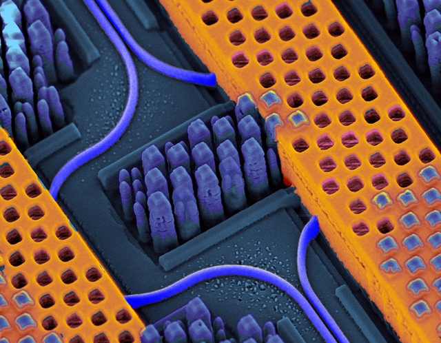 Shown in blue are the optical waveguides (and bend radius) while the copper wires carrying high-speed electrical signals are shown in orange. Source: IBM
System vendors have been on a silicon-photonics spending spree.
Cisco Systems started the ball rolling in 2012 when it acquired silicon photonics start-up, LightWire, for $272M. Mellanox Technologies more recently bought Kotura for $82M. Now Huawei has acquired Caliopa, a four-year-old Belgium-based start-up, for an undisclosed fee. The Chinese system vendor has said it is looking to further bolster its European R&D, and highlighted silicon photonics in particular.
Given that it was only just over a decade ago when systems companies were shedding their optical component units, the trend to acquire silicon photonics highlights the growing importance of the fledgling technology.
These system vendors view silicon photonics as a strategic technology. The equipment makers want to develop expertise and experience as they plan to incorporate the technology in upcoming, hopefully differentiated platforms.
"If I have a Terabit of capacity on the front panel, how am I going to manipulate that across the line card, a fabric or the backplane?" says Adam Carter, general manager and senior director of the transceiver modules group at Cisco Systems. "We saw silicon photonics as a technology that could potentially enable us to get there."
System vendors are already using embedded optics - mounted on boards close to the ICs instead of pluggable modules on the front panel - to create platforms with denser interfaces.
"Photonics doesn't need the latest and greatest lithography"
Arista Networks' 7500E switch has a line card with board-mounted optics rather than pluggable transceivers to increase 100 Gigabit port density. The company offers several line cards using pluggable modules but it has designed one card with board-mounted optics that offers flexible interfaces - 10 Gig, 40 Gig and 100 Gig - and a higher port density. When developing the design, the multi-source agreement (MSA) CFP2 pluggable module was not ready, says Arista.
Compass-EOS, a core IP router start-up, has developed chip-mounted optics based on 168 lasers and 168 detectors. The novel Terabit-plus optical interface removes the need for a switch fabric and the mid-plane to interconnect the router card within the platform. The interface also enables linking of platforms to scale the IP core router.
Both companies are using VCSELs, an established laser technology that silicon photonics competes with. Yet the two designs highlight how moving optics closer to chips enables system innovation, a development that plays to silicon photonics' strength.
 "I characterise silicon photonics as a technology that will compete in the right applications but won’t displace indium phosphide" Ed Murphy, JDSU
Silicon photonics promises cost savings by enabling vendors to piggyback on the huge investments made by the semiconductor industry. Vendors making their own products, such as optical transceivers, also promises to shake up the existing optical component supply chain.
Cisco Systems' first silicon photonics product is the proprietary 100 Gigabit optical CPAK transceiver that is undergoing qualification. By making its own optical module, Cisco avoids paying the optical module makers' margins. Cisco claims the CPAK's smaller size improves the faceplate density compared to the CFP2.
Pros and cons
Silicon photonics may be able to exploit the huge investment already made in the semiconductor industry, but it does differ from standard CMOS integrated circuits (ICs).
First, optics does not have the equivalent of Moore's Law. Whereas chip economics improve with greater integration, only a few optical functions can be cascaded due to the accumulated signal loss as light travels through the photonic circuit. This is true for optical integration in general, not just silicon photonics.
Another issue is that the size of an optical component - a laser or a modulator - is dictated by the laws of physics rather than lithography. "Photonics doesn't need the latest and greatest lithography," says Martin Zirngibl, domain leader for enabling physical technologies at Alcatel-Lucent's Bell Labs. "You can live with 100nm, 120nm [CMOS] components whereas for electronics you want to have 45nm."
This can lead to the interesting situation when integrating electronics with photonics. "You either don't use the latest technology for electronics or you waste a lot of real estate with very expensive lithography for photonics," says Zirngibl.
Another disadvantage of silicon is that the material does not lase. As a result, either a III-V material needs to be bonded to the silicon wafer or an external laser must be coupled to the silicon photonics circuit.
Silicon also has relatively small waveguides which make it tricky to couple light in and out of a chip.
The advantages of silicon photonics, however, are significant.
The technology benefits from advanced 8- and 12-inch wafers and mature manufacturing processes developed by the semiconductor industry. Using such CMOS processes promises high yields, manufacturing scale, and automation and testing associated with large scale IC manufacturing.
"This is probably the only advantage but it is very significant," says Valery Tolstikhin, founder and former CTO of indium phosphide specialist, OneChip Photonics, and now an independent consultant. "It takes silicon totally off the scale compared to any other photonics materials."
"We can build the single-die optical engine in the same CMOS line where processors are built, where billions [of dollars] of investment has been done"
IBM's high-density silicon photonics optical engine is made using a 90nm CMOS process. "We can build the single-die optical engine in the same CMOS line where processors are built, where billions [of dollars] of investment has been done," says Yurii Vlasov, manager of the silicon nanophotonics department at IBM Research. "We are riding on top of that investment."
Extra processing may be introduced for the photonics, says IBM, but the point is that there is no additional capital investment. "It is the same tooling, the same process conditions; we are changing the way this tooling is used," says Vlasov. "We are changing the process a little bit; the capital investment is in place."
 "We believe that even for shorter distance, silicon photonics does compete in terms of cost with VCSELs." Yurii Vlasov, IBM
Stephen Krasulick, CEO of silicon photonics start-up, Skorpios Technologies, makes a similar point. "The real magic with our approach is the ability to integrate it with standard, commercial fabs," he says.
Skorpios is a proponent of heterogeneous integration, or what the company refers to as 'silicon photonics 2.0'. Here silicon and III-V are wafer-bonded and the optical components are created by etching the two materials. This avoids the need to couple external lasers and to use active alignment.
"We do it in a manner such that the CMOS foundry is comfortable letting the wafer back into the CMOS line," says Krasulick, who adds that Skorpios has been working with CMOS partners from the start to ensure that its approach suits their manufacturing flow.
Applications
The first applications adopting silicon photonics span datacom and telecom: from short-reach interconnect in the data centre to 100 Gigabit-per-second (Gbps) long-distance coherent transmission.
Intel is developing silicon photonics technology to help spur sales of its microprocessors. The chip giant is a member of Facebook's Open Compute Project based on a disaggregated system design that separates storage, computing and networking. "When I upgrade the microprocessors on the motherboard, I don't have to throw away the NICs [network interface controllers] and disc drives," says Victor Krutul, director business development and marketing for silicon photonics at Intel. The disaggregation can be within a rack or span rows of equipment.
"Optical modules do not require state-of-the-art lithography or large scale photonic integration, but they do need to be coupled in and out of fibre and they need lasers - none of that silicon photonics has a good solution for"
Intel has developed the Rack Scale Architecture (RSA) which implements a disaggregated design. One RSA implementation for Facebook uses three 100Gbps silicon photonics modules per tray. Each module comprises four transmit and four receive fibres, each at 25Gbps. Each tray uses a Corning-developed MXC connector and its ClearCurve fibre that support data rates up to 1.6Tbps. “Different versions of RSA will have more or less modules depending on requirements," says Krutul.
Luxtera, whose silicon photonics technology has been used for active optical cables, and Mellanox's Kotura, are each developing 100Gbps silicon photonics-based QSFPs to increase data centre reach and equipment face plate density.
One data centre requirement is the need for longer reach links. VCSEL technology is an established solution but at 100Gbps its reach is limited to 100m only. Intel's 100Gbps module, operating at 1310nm and combined with Corning's MXC connector and ClearCurve multi-mode fibre, enables up to 300m links. But for greater distances - 500m to 2,000m - a second technology is required. Data centre managers would like one technology that spans the data centre yet is cost competitive with VCSELs.
"Silicon photonics lends itself to that," says Cisco's Carter. "If we drive the cost lower, can we start looking at replacing or future proofing your network by going to single mode fibre?"
 "There are places where silicon photonics will definitely win, such as chip-to-chip optical interconnects, and there are places where there is still a question mark, like fibre-optics interconnects." Valery Tolstikhin
IBM's 25Gbps-per-channel optical engine has been designed for use within data centre equipment. "We are claiming we have density based on optical scaling which is the highest in the industry, and we have done it using monolithic integration: optical devices are built side-by-side with CMOS," says Vlasov.
What is important, says Vlasov, is not so much the size of the silicon waveguide but how sharp its bend radius is. The bend radius dictates how sharply the light can be guided while remaining confined within the integrated circuit. The higher the light confinement, the smaller the bend radius and hence the overall circuit area.
Much progress has been made in improving light confinement over the past two decades, resulting in the bend ratio coming down from 1cm to a micron. IBM claims that with its technology, it can build systems comprising hundreds of devices occupying a millimeter. "That is a major difference in the density of optical integration," says Vlasov.
IBM does not use heterogeneous integration but couples lasers externally."It is not complicated, it is a technical problem we are solving; we believe that is the way to go," says Vlasov. "The reason why we have gone down this path is very simple: we believe in monolithic integration where electrical circuitry sits side by side with optical components."
Such monolithic integration of the optics with the electronics, such as modulator drivers and clock recovery circuitry, reduces significantly the cost of packaging and testing. "We believe that even for shorter distances, silicon photonics does compete in terms of cost with VCSELs if all elements of the cost are taken care of: bill of materials, packaging and testing," says Vlasov.
But not everyone believes silicon photonics will replace VCSELs.
For example, Tolstikhin questions the merits of silicon photonics for transceiver designs, such as for 100 Gig modules in the data centre. "There are places where silicon photonics will definitely win, such as chip-to-chip optical interconnects, and there are places where there is still a question mark, like fibre-optics interconnects," he says.
Tolstikhin argues that silicon photonics offers little advantage for such applications: "Optical modules do not require state-of-the-art lithography or large scale photonic integration, but they do need to be coupled in and out of fibre and they need lasers - none of that silicon photonics has a good solution for."
Cisco says it was first attracted to LightWire's technology because of its suitability for optical transceivers. Six years ago 1W, SFP+ modules were limited to 10km. "Customers wanted 40km, 80km, even WDM," says Carter. "They [LightWire] did a 40km SFP+ using their modulator that consumed only 0.5W - a huge differentiator." Two years ago 100 Gig CFP modules were at 24W while LightWire demonstrated a module under 8W, says Carter.
Tolstikhin believes silicon photonics' great promise is for applications still to emerge. One example is chip-to-chip communication that has modest optical light requirements and does not have to be coupled in and out of fibre.
"Here you have very high requirements for density packaging and the tiny [silicon] waveguides are handy whereas indium phosphide is too big and too expensive here," says Tolstikhin. Longer term still, silicon photonics will be used for on-chip communication but that will likely be based on deep sub-wavelength scale optics such as surface plasmonics rather than classical dielectric waveguides.
Tolstikhin also argues that the economics of using indium phosphide compared to silicon photonics need not be all that gloomy.
Indium phosphide is associated with custom small-scale fabs and small volume markets. But indium phosphide can benefit from the economics of larger industries just as silicon photonics promises to do with the semiconductor industry.
Indium phosphide is used in higher volume for wireless ICs such as power amplifiers. "Quite significantly orders of magnitude higher," says Tolstikhin. The issue is that, conventionally, photonic circuits are fabricated by using multiple epitaxial growth steps, whereas the wireless ICs are made in a single-growth process, hence epitaxy and wafer processing are decoupled.
"If you can give up on regrowth and still preserve the desired photonic functionality, then you can go to commercial RF IC fabs," he says. "This is a huge change in the economic model." It is an approach that enables a fabless model for indium phosphide photonics, with the potential advantages not unlike those claimed by silicon photonics with respect to commercial CMOS fabs.
"That suggests indium phosphide - which has all kinds of physical advantages for those applications that require transmitters, receivers and fibre, plus readily available high-speed analogue electronics for trans-impedance amplifiers and laser or modulator drivers - may be quite a competitive contender," says Tolstikhin.
"Silicon photonics has a certain capability but the hype around it has magnified that capability beyond reality"
Customers don't care which technology is used inside a transceiver. "They care only about cost, power and package density," says Tolstikhin. "Indium phosphide can be competitive and on many occasions beat silicon photonics."
JDSU also believes that long-term, a perfect fit for silicon photonics may be relative short reach interconnects – chip-to-chip and board-to-board reaches. “You need to have very high speed and dense interconnects, I can see that as being a very strong value proposition long term," says Ed Murphy, senior director, communications and commercial optical products at JDSU.
Finisar and JDSU are open to the potential benefits of silicon photonics but remain strong proponents of traditional optical materials such as indium phosphide and gallium arsenide.
"We have designed silicon photonic chips here at Finisar and have evaluations that are ongoing. There are many companies that now offer silicon photonics foundry services. You can lay out a chip and they will build it for you," says Jerry Rawls, executive director of Finisar. "The problem is we haven't found a place where it can be as efficient or offer the performance as using traditional lasers and free-space optics."
"Silicon photonics has a certain capability but the hype around it has magnified that capability beyond reality,” says JDSU's Murphy. "Practitioners of silicon photonics would tell you that as well."
According to Murphy, each application, when looked at in detail, has its advantages and disadvantages when using either silicon photonics or indium phosphide. “Even in those applications where one or the other is better, the level of improvement is measured in a few tens of percent, not factors of ten,” he says. "I characterise silicon photonics as a technology that will compete in the right applications but won’t displace indium phosphide."
Silicon photonics for telecom
At the other extreme of the optical performance spectrum, silicon photonics is being developed for long-distance optical transmission. The technology promises to help shrink coherent designs to fit within the CFP2 module, albeit at the expense of reach. A CFP2 coherent module has extremely challenging cost, size and power requirements.
Teraxion is developing a coherent receiver for CFP2. "We believe silicon photonics is the material of choice to fulfill CFP2 requirements while allowing even smaller size reduction for future modules such as the CFP4," said Martin Guy, Teraxion's vice president of product management and technology.
u2t Photonics and Finisar recently licensed indium phosphide modulator technology to help shrink coherent designs into smaller form factor pluggables. So what benefit does silicon photonics offer here?
"In terms of size there will not be much difference between indium phosphide and silicon photonics technology," says Guy. "However, being on each side on the fence, we know that process repeatability and therefore yield is better with silicon photonics." Silicon photonics thus promises a lower chip cost.
"We have projects spanning everything from access all the way to long haul, and covering some datacom as well," says Rob Stone, vice president of marketing and program management at Skorpios. The start-up has developed a CMOS-based tunable laser with a narrow line width that is suitable for coherent applications.
"If you develop a library of macrocells, you can apply them to do different applications in a straightforward manner, provided all the individual macrocells are validated," says Stone. This is different to the traditional design approach.
Adding a local oscillator to a coherent receiver requires a redesign and a new gold box. "What we've got, we can plug things together, lay it out differently and put it on a mask," says Stone. "This enables us to do a lot of tailoring of designs really quite quickly - and a quick time-to-market is important."
Perhaps the real change silicon photonics brings is a disruption of the supply chain, says Zirngibl.
An optical component maker typically sells its device to a packaging company that puts it in a transmitter or receiver optical sub-assembly (TOSA/ ROSA). In turn, the sub-assemblies are sold to a module company which then sells the optical transceiver to an equipment vendor. Each player in the supply chain adds its own profit.
Silicon photonics promises to break the model. A system company can design its own chip using design tools and libraries and go to a silicon foundry. It could then go to a packaging company to make the module or package the device directly on a card, bypassing the module maker altogether.
Yet the ASIC model can also benefit module makers.
IBM has developed its 25Gbps-per-channel silicon photonics technology for its platforms, for chip-to-chip and backplanes, less for data centre interconnect. But it is open to selling the engine to interested optical module players. "If this technology can be extended to 2km for big data centres, others can come in, the usual providers of transceivers," says Vlasov.
"There are companies with the potential to offer a [silicon photonics] design service or foundry service to others that would like to access this technology," says Cisco's Carter. "Five years ago there wasn't such an ecosystem but it is developing very fast."
The article is an extended version of one that appeared in the exhibition magazine published at ECOC 2013.
Part 1: Optical interconnect, click here
Part 2: Bell Labs on silicon photonics, click here
OFC/NFOEC 2013 industry reflections - Part 4
Gazettabyte asked industry figures for their views after attending the recent OFC/NFOEC show.
"Spatial domain multiplexing has been a hot topic in R&D labs. However, at this year's OFC we found that incumbent and emerging carriers do not have a near-term need for this technology. Those working on spatial domain multiplexing development should adjust their efforts to align with end-users' needs"
T.J. Xia, Verizon
T.J. Xia, distinguished member of technical staff, Verizon
Software-defined networking (SDN) is an important topic. Looking forward, I expect SDN will involve the transport network so that all layers in the network are controlled by a unified controller to enhance network efficiency and enable application-driven networking.
Spatial domain multiplexing has been a hot topic in R&D labs. However, at this year's OFC we found that incumbent and emerging carriers do not have a near-term need for this technology. Those working on spatial domain multiplexing development should adjust their efforts to align with end-users' needs.
Several things are worthy to watch. Silicon photonics has the potential to drop the cost of optical interfaces dramatically. Low-cost pluggables such as CFP2, CFP4 and QSFP28 will change the cost model of client connections. Also, I expect adaptive, DSP-enabled transmission to enable high spectral efficiencies for all link conditions.
Andrew Schmitt, principal analyst, optical at Infonetics Research
The Cisco CPAK announcement was noteworthy because the amount of attention it generated was wildly out of proportion to the product they presented. They essentially built the CFP2 with slightly better specs.
"It was very disappointing to see how breathless people were about this [CPAK] announcement. When I asked another analyst on a panel if he thought Cisco could out-innovate the entire component industry he said yes, which I think is just ridiculous."
Cisco has successfully exploited the slave labour and capital of the module vendors for over a decade and I don't see why they would suddenly want to be in that business.
The LightWire technology is much better used in other applications than modules, and ultimately the CPAK is most meaningful as a production proof-of-concept. I explored this issue in depth in a research note for clients.
It was very disappointing to see how breathless people were about this announcement. When I asked another analyst on a panel if he thought Cisco could out-innovate the entire component industry he said yes, which I think is just ridiculous.
There were also some indications surrounding CFP2 customers that cast doubt on the near-term adoption of the technology, with suppliers such as Sumitomo Electric deciding to forgo development entirely in favour of CFP4 and/ or QSFP.
I think CFP2 ultimately will be successful outside of enterprise and data centre applications but there is not a near-term catalyst for adoption of this format, particularly now that Cisco has bowed out, at least for now.
SDN is a really big deal for data centres and enterprise networking but its applications in most carrier networks will be constrained to only a few areas relative to multi-layer management.
Within carrier networks, I think SDN is ultimately a catalyst for optical vendors to potentially add value to their systems, and a threat to router vendors as it makes bypass architectures easier to implement.
"Pluggable coherent is going to be just huge at OFC/NFOEC 2014"
Optical companies like ADVA Optical Networking, Ciena and Infinera are pushing the envelope here and the degree to which optical equipment companies are successful is dependent on who their customers are and how hungry these customers are for solutions.
Meanwhile, pluggable coherent is going to be just huge at OFC/NFOEC 2014, followed by QSFP/ CFP4 prototyping and more important production planning and reliability. Everyone is going to use different technologies to get there and it will be interesting to see what works best.
I also think the second half of 2013 will see an increase in deployment of common equipment such as amplifiers and ROADMs.
Magnus Olson, director hardware engineering, Transmode
Two clear trends from the conference, affecting quite different layers of the optical networks, are silicon photonics and SDN.
"If you happen to have an indium phosphide fab, the need for silicon photonics is probably not that urgent. If you don't, now seems very worthwhile to look into silicon photonics"
Silicon photonics, deep down in the physical layer, is now emerging rapidly from basic research to first product realisation. Whereas some module and component companies barely have taken the step from lithium niobate modulators to indium phospide, others have already advanced indium phosphide photonic integrated circuits (PICs) in place.
If you happen to have an indium phosphide fab, the need for silicon photonics is probably not that urgent. If you don't, now seems very worthwhile to look into silicon photonics.
Silicon photonics is a technology that should help take out the cost of optics for 100 Gigabit and beyond, primarily for short distance, data centre applications.
SDN, on the other hand, continues to mature. There is considerable momentum and lively discussion in the research community as well as within the standardisation bodies that could perhaps help SDN to succeed where Generalized Multi-Protocol Label Switching (GMPLS) failed.
Ongoing industry consolidation has reduced the number of companies to meet and discuss issues with to a reasonable number. The larger optical module vendors all have full portfolios and hence the consolidation would likely slow down for awhile. The spirit at the show was quite optimistic, in a very positive, sustainable way.
As for emerging developments, the migration of form factors for 100 Gigabit, from CFP via CFP2 to CFP4 and beyond, is important to monitor and influence from a wavelength-division multiplexing (WDM) vendor point of view.
We should learn from the evolution of the SFP+, originally invented with purely grey data centre applications. Once the form factor is well established and mature, coloured versions start to appear.
If not properly taken into account from the start in the multi-source agreement (MSA) work with respect to, for example, power classes, it is not easy to accommodate tunable dense WDM versions in these form factors. Pluggable optics are crucial for cost as well as flexibility, on both the client side and line side.
Shai Rephaeli, vice president of interconnect products, Mellanox
At OFC, many companies demonstrated 25 Gigabit-per-second (Gbps) prototypes and solutions, both multi mode and single mode.
Thus, a healthy ecosystem for the 100 Gigabit Ethernet (GbE) and EDR (Enhanced Data Rate) InfiniBand looks to be well aligned with our introduction of new NIC (network interface controller)/ HCA (Infiniband host channel adaptor) and switch systems.
However, a significant increase in power consumption compared to current 10Gbps and 14Gbps product is observed. This requires the industry to focus heavily on power optimisation and thermal solutions.
"One development to watch is 1310nm and 1550nm VCSELs"
Standardisation for 25Gbps single mode fibre solutions is a big challenge. All the industry leaders have products at some level of development, but each company is driving its own technology. There may be a real interoperability barrier, considering the different technologies: WDM/ 1310nm, parallel and pulse-amplitude modulation (PAM) which, itself, may have several flavours: 4-levels, 8-levels and 16-levels.
One development to watch is 1310nm and 1550nm VCSELs, which can bring the data centre/ multi-mode fibre volume and prices into the mid-reach market. This technology can be important for the new large-scale data centres, requiring connections significantly longer than 100m.
Part 1: Software-defined networking: A network game-changer, click here
Part 2: OFC/NFOEC 2013 industry reflections, click here
Part 3: OFC/NFOEC 2013 industry reflections, click here
Part 5: OFC/NFEC 2013 industry reflections, click here
OFC/NFOEC 2013 product round-up - Part 1
Part 1: Client-side transceivers
- First CFP2 single-mode and multi-mode transceiver announcements
- Cisco Systems unveils its CPAK module
- 100 Gigabit QSFPs from Kotura and Luxtera
- CFP2 and 40km CFP 10x10 MSA modules
- Infiniband FDR and 'LR4 superset' QSFPs
The recent OFC/NFOEC exhibition and conference held in Anaheim, California, saw a slew of optical transceiver announcements. The first CFP2 client-side products for single-mode and multi-mode fibre were unveiled by several companies, as was Cisco Systems' in-house CPAK transceiver.
The CFP2 is the pluggable form factor that follows the first generation CFP. The CFP MSA announced the completion of the CFP2 specification at the show, while several vendors including Avago Technologies, Finisar, Fujitsu Optical Components, NeoPhotonics, Oclaro and Oplink Communications detailed their first CFP2 products.
The 40 and 100 Gigabit CFP2 is half the size of the CFP, enabling at least a doubling of the CFP2 transceivers on a faceplate compared to four CFPs (see table below). The CFP2 is also future-proofed to support 200 and 400Gbps (See first comment at bottom of CFP2 story).
Another difference between the CFP and the CFP2 is that the CFP2 uses a 4x25Gbps electrical interface. Accordingly, the CFP2 does not need the 'gearbox' IC that translates between ten, 10 Gigabit-per-second (Gbps) lanes to four, 25Gbps electrical lanes that interface to the 4x25/28Gbps optics. Removing the gearbox IC saves space and reduces the power consumption by several watts.
The industry has long settled on the SFP+ at 10Gbps while the QSFP has become the 40Gbps form factor of choice. With 100Gbps still in its infancy, transceiver vendors are pursuing several client-side interfaces. Much work will be needed to reduce the size, power consumption and cost of 100Gbps interfaces before the industry settles on a single pluggable form factor for the single-mode and multi-mode standards.
CFP2 announcements
Finisar demonstrated two CFP2 modules, one implementing the IEEE 100GBASE-LR4 10km standard and the other, the IEEE 100GBASE-SR10 100m multi-mode standard. The company is using directly-modulated, distributed feedback (DFB) lasers for its CFP2 LR4. In contrast, the CFP module uses more expensive, electro-absorption modulator lasers (EMLs). Finisar demonstrated interoperability between the two LR4 modules, an EML-based CFP and a DFB-based CFP2, at the show.
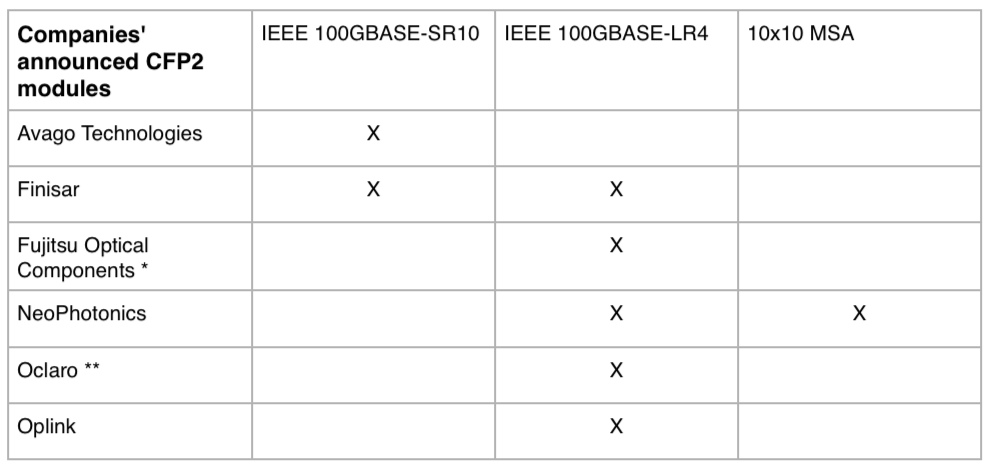
* An ER4 CFP2 is under development
** Oclaro disclosed indium phosphide components for a future CFP2 line side pluggable
Using directly modulated lasers also reduces the power consumption, says Finisar. Overall, the CFP2 LR4 consumes 7W compared to a 24W first-generation CFP-based LR4.
"We can migrate these [directly modulated laser] designs to a single quad 28 Gig photonic integrated circuit TOSA," says Rafik Ward, Finisar's vice president of marketing. "Likewise on the receive [path], there will be a quad 28 Gig ROSA." The TOSA refers to a transmitter optical sub-assembly while the ROSA is the receiver equivalent. Ward says the CFP2s will be in production this year.
Several module and chip makers took part in the Optical Internetworking Forum's (OIF) multi-vendor demonstration of its 4x25 Gigabit chip-to-module electrical interface, the CEI-28G-VSR. The demonstration included CFP2 LR4s from Finisar and from Oclaro as well as Luxtera's 100Gbps shorter reach module in a QSFP28. Oclaro's CFP2 is expected to be in production in the third quarter of 2013.
Another standard implemented in the CFP2 is the 100GBASE-SR10 multi-mode standard. Avago Technologies and Finisar both detailed CFP2 SR10 modules. The SR10 uses 10 VCSELs, each operating at 10Gbps. The SR10 can be used as a 100Gbps interface or as 10 independent 10Gbps channels.
The CFP2 SR10 can be interfaced to 10 Gigabit Ethernet (GbE) SFP+ modules or combinations of 10GbE SFP+ and 40GbE QSFPs. "What people are looking for using the CFP2 multi-mode module is not only for the 100 Gig Ethernet application but interoperability with 40 Gig Ethernet as well as 10 Gig Ethernet modules," says I Hsing Tan, Ethernet segment marketing manager in the fibre optics product division at Avago.
The SR10 electrical interface specification supports retiming and non-retiming options. The Avago CFP2 module includes clock data recovery ICs that can be used for retiming if needed or bypassed. The result is that Avago's CFP2 SR10 consumes 4-6W, depending on whether the clock data recovery chips are bypassed or used.
Meanwhile, NeoPhotonics became the first company to announce the 10x10 MSA in a CFP2.
NeoPhotonics has not detailed the power consumption but says the 10x10Gbps CFP2 is lower than the CFP since all of the chips - photonic and electrical - are a newer generation and much work has gone into reducing the power consumption.
"Demand is quite strong for the 10x10 solution," says Ferris Lipscomb, vice president of marketing at NeoPhotonics. "The CFP2 version is being developed, and we expect strong demand there as well."
The key advantage of the 10x10-based solution over a 4x25Gbps design is cost, according to NeoPhotonics. "10x10 enjoys the volume and maturity of 10 Gig, and thus the cost advantage," says Lipscomb. "We believe the 10x10 CFP2 will follow the trend of the 10x10 MSA CFP and will offer a significant cost advantage over CFP2 LR4-based solutions."
Cisco's CPAK
Cisco finally showed its in-house silicon photonics-based CPAK transceiver at OFC/NFOEC. The CPAK is the first product to be announced following Cisco's acquisition of silicon photonics player, LightWire.

Cisco says the CPAK is more compact than the CFP2 transceiver with the company claiming that 12 or more transceivers will fit on a faceplate. "While the industry is leapfrogging the CFP with the CFP2, our CPAK leapfrogs the CFP2 because it is much more efficient from a size and power consumption perspective," says Sultan Dawood, a marketing manager at Cisco.
Vendors backing the CFP2 stress that the CPAK is only slighter smaller than the MSA module. "The CFP2 and the CPAK are both interim form factors pending when the CFP4 becomes available." says Avago's Tan. "Any product [like the CFP2] governed by an MSA is going to see strong market adoption."
 Cisco's CPAK transceiver Source: Cisco
The CFP4 specification is still being worked on but 16 CFP4s will fit on a faceplate and the transceiver is scheduled for the second half of 2014.
At OFC, Cisco demonstrated the CPAK implementing the 100GBASE-LR4 and -SR10 standards. The CPAK transceiver will be generally available in the summer of 2013, says Cisco.
CFP
Oplink Communication and hybrid integration specialist, Kaiam, showed a 100Gbps 10x10 MSA CFP implementing a 40km extended reach.
The 10x10 40km CFP is for connecting data centres and for broadband backhaul applications. The CFP electro-absorption modulator lasers coupled to a wavelength multiplexer make up the TOSA while the ROSA comprises avalanche photodiode receivers and a demultiplexer. Samples will be available in the second quarter of 2013, with production starting in the third quarter.
Source Photonics announced a second-generation 100GBASE-LR4 CFP with a power consumption of 12-14W.
Meanwhile, Effdon Networks detailed its first 100Gbps product, a CFP with a reach of 80km. Until now 100Gbps CFPs have been limited largely to 10km LR4 while the first 100Gbps CFPs with a reach of 80km or greater being 4x25Gbps direct-detection designs that can include specialist ICs.
100 Gig QSFP
Luxtera and Kotura, both detailed 100 Gigabit QSFPs that use their respective silicon photonics technology. The Kotura design uses two chips, has a reach of 2km and is a four-channel wavelength-division multiplexing (WDM) design while the Luxtera design is a four-channel integrated transceiver that uses a single laser and is tailored for 500m although Luxtera says it can achieve a 2km reach.
40 Gigabit Ethernet and Infiniband FDR
Avago Technologies announced that its eSR4 40 Gigabit Ethernet (GbE) QSFP+ has a reach of up to 550m, beyond the reach specified by the IEEE 40GBASE-SR4 standard. The eSR4 supports 40GbE or four independent 10GbE channels. When used as a multi-channel 10GbE interface, the QSFP+ interfaces to various 10GbE form factors such as X2, XFP and SFP+, It can also interface to a 100GbE CFP2, as mentioned.
Avago first announced the eSR4 QSFP+ with a reach of 300m over OM3 multi-mode fibre and 400m over OM4 fibre. The eSR4 now extends the reach to a guaranteed 550m when used with specific OM4 fibre from fibre makers Corning, Commscope and Panduit.
The extended reach is needed to address larger data centres now being build, as well as support flatter switch architectures that use two rather than three tiers of switches, and that have greater traffic flowing between switches on the same tier.
Avago says data centre managers are moving to deploy OM4 fibre. "The end user is going to move from OM3 to OM4 fibre for future-proofing purposes," says Tan. "The next-generation 32 Gig Fibre Channel and 100 Gigabit Ethernet are focussing on OM4 fibre."
Meanwhile, ColorChip showed its 56Gbps QSFP+ implementing the FDR (Fourteen Data Rate) 4x Infiniband standard as part of a Mellanox MetroX long-haul system demonstration at the show.
Finisar also demonstrated a 40Gbps QSFP using four 1310nm VCSELs. The result is a QSFP with a 10km reach that supports a 40Gbps link or four, 10Gbps links when used in a 'breakout' mode. The existing 40GBASE-LR4 standard supports a 40Gbps link only. Finisar's non-standard implementation adds a point-to-multipoint configuration.
"A single form factor port can be used not only for 40 Gig but also can enable higher density 10 Gig applications than what you can do with SFP+," says Ward.
Kaiam detailed a 40Gbps QSFP+ ER4 transceiver having a 40km reach. The QSFP+ transceiver has the equivalent functionality of four DML-based SFP+s fixed on a coarse WDM grid, and includes a wavelength multiplexer and de-multiplexer.
For OFC/NFOEC 2013 - Part 2, click here
Further reading
LightCounting: OFC/NFOEC review: news from the show floor, click here
Ovum: Cisco hits both show hot buttons with silicon photonics for 100G, click here
OFC/NFOEC 2013 industry reflections - Part 2
Bill Gartner, vice president and general manager of high-end routing and optical business unit at Cisco Systems.
There were several key themes during this year’s OFC conference, but what I found most compelling were the disruptive trends and technologies that stand to significantly impact the optical communications market in the coming years.

"SDN could be the single biggest disruptor in the transport industry and has the potential to transform network programmability and orchestration"
One of the hottest themes at this year’s OFC conference is the role of silicon photonics and the benefits it presents to service providers and carriers. Silicon photonics is truly one of the most interesting advancements taking place in the industry as it has the potential to drastically lower the density, power and overall cost of ASICs.
Several carriers at the show, including CenturyLink and AT&T, presented their view that optics is becoming a larger portion of their spend and now exceeds the cost of packet switching technologies.
A second key trend coming out of the show is software-defined networking (SDN) and its impact on networking. There is tremendous industry interest around this topic and it extended to the Anaheim Convention Center.
With SDN, our customers can increase flexibility in terms of selecting the features and protocols that make sense for their network application – whether it is a data centre application, a service provider application or a large-scale enterprise application.
The last theme that resonated during OFC was around the convergence of packet and optical solutions. As service providers look for ways to decrease both CapEx and OpEx related to the network, incremental technology improvements will decrease costs. However, for many customers, their network capacity is growing far faster than their revenues, so incremental improvements will not yield required reductions.
"As an industry we have to evolve organisationally and technically. Those who fail to recognise that face extinction."
This shows us that we need to explore more fundamental shifts in architectures that have the potential to yield significant savings in OpEx and CapEx. Enter the convergence of IP and optical – this may take the form of converged platforms, but will also involve multi-layer control planes that allow the exchange of information between the packet and optical layers. This convergence helps answer questions like: How well is the network utilised? Can it be optimised? Are there multi-layer protection/ restoration schemes that make better use of the available resources?
During the conference, I had the opportunity to present at the OSA Executive Forum, which brought together more than 150 senior-level executives to discuss key themes, opportunities and challenges facing the next generation in optical communications.
What struck me is that this industry is constantly evolving, which presents challenges and opportunities. We are looking at an industry that is highly fragmented at the moment and requires further streamlining.
You have new players at every level of the value chain that bring exciting, unique perspectives and advanced technologies that increase efficiency and decrease costs. But none of this innovation comes without change; as an industry we have to evolve organisationally and technically. Those who fail to recognise that face extinction.
"This is like solving a simultaneous equation where the variables are power, cost and density – you need to solve for all three"
The key themes discussed at OFC are an indication of what is to come in optical transport and mirror our top priorities at Cisco.
In the coming year, we expect to see CMOS photonics technology enable lower power pluggables. This is the case with CPAK, but more broadly, we will see this technology find its way into low cost board-to-board interconnect and chassis-to-chassis interconnect.
As an industry, we have made great progress in reducing the cost of transmitting bits over a long distance but much more remains to be done. As bit rates increase to beyond 100 Gigabit, we must look for ways to drive this cost down faster, while decreasing both power and size. This is like solving a simultaneous equation where the variables are power, cost and density – you need to solve for all three.
During the next five years, I think that SDN could be the single biggest disruptor in the transport industry and has the potential to transform network programmability and orchestration.
We will see an entire software industry emerge around SDN, but it is important to note that this is really all about multilayer control – Layer 0 to Layer 3. SDN is not simply an optical transport problem to be solved. The advantage will go to those who are looking at this holistically.
Brandon Collings, CTO of the communications and commercial optical products group at JDSU
I found it interesting that the major network equipment manufactures had a significantly increased presence on the exhibition floor.

"This year’s focus and buzz was all on silicon photonics with researchers leveraging it against nearly every function in telecom and datacom"
I learned a lot about SDN at levels above the photonic network. This is a very complex topic likely to take some time to fully mature within telecom networks; however, the potential values appear compelling.
This year’s focus and buzz was all on silicon photonics with researchers leveraging it against nearly every function in telecom and datacom. I expect it will be interesting for industry watchers how this promising technology evolves within the industry, where it achieves its promise and where it runs into practical roadblocks.
Vladimir Kozlov, CEO of LightCounting
This was the best OFC since 2000. The optical community is once again energised. Some attribute the improved mood to high-value acquisitions of companies LightWire and Nicira that were made last year, but this is just part of the story.
Yes, the potential of silicon photonics and software-defined networking (which LightWire and Nicira were focussed on, respectively) do broaden the horizon for optical technologies in communication networks and data centres. But the excitement is not limited to just these two ideas. All the new - and old or forgotten - ideas, technologies and products once again have a shot at making a difference. Demand for optics is strong and the customers are hungry for innovation.
"Demand for optics is strong and the customers are hungry for innovation"
In contrast to 2000, few people are getting carried away with the excitement. The mood is much more constructive this time and it makes me hope that most of this new energy will not be wasted.
I would not single out a specific technology or application to watch out for in the next few years. All of them have opportunities and challenges ahead. We will keep track of as many developments as we can and make sure that hype does lead the industry off the tracks this time.
Effie Favreau, marketing, Sumitomo Electric
One hundred Gigabit technology is here. Last year there was a lot of hype about 100 Gigabit and now it is reality; vendors have products that are shipping.
Sumitomo and ClariPhy partnered on pluggable coherent modules. Together, we hosted an impressive demonstration with all the components to make pluggable coherent modules available next year.
"For the enterprise/ data centre, vendors requiring low cost, high density equipment really need the CFP4"
One thing I learned from the show is that vendors need to re-purpose their existing equipment. There was much discussion regarding software-enabled applications and passives to enhance the performance of networks and make them more intelligent.
There was the introduction of the CFP2 from several vendors as well as Cisco's CPAK. For the enterprise/ data centre, vendors requiring low cost, high density equipment really need the CFP4. At Sumitomo, we are concentrating our R&D efforts on the CFP4.
See also:
Part 1: Software-defined networking: A network game-changer? click here
Part 3: OFC/NFOEC 2013 industry reflections, click here
Part 4: OFC/NFOEC industry reflections, click here
Part 5: OFC/NFEC 2013 industry reflections, click here
Luxtera's interconnect strategy
Part 1: Optical interconnect
Luxtera demonstrated a 100 Gigabit QSFP optical module at the OFC/NFOEC 2013 exhibition.
 "We're in discussions with a lot of memory vendors, switch vendors and different ASIC providers"
Chris Bergey, Luxtera
The silicon photonics-based QSFP pluggable transceiver was part of the Optical Internetworking Forum's (OIF) multi-vendor demonstration of the 4x25 Gigabit chip-to-module interface, defined by the CEI-28G-VSR Implementation Agreement.
The OIF demonstration involved several optical module and chip companies and included CFP2 modules running the 100GBASE-LR4 10km standard alongside Luxtera's 4x28 Gigabit-per-second (Gbps) silicon photonics-based QSFP28.
Kotura also previewed a 100Gbps QSFP at OFC/NFOEC but its silicon photonics design uses two chips and wavelength-division multiplexing (WDM).
The Luxtera QSFP28 is being aimed at data centre applications and has a 500m reach although Luxtera says up to 2km is possible. The QSFP28 is sampling to initial customers and will be in production next year.
100 Gigabit modules
Current 100GBASE-LR4 client-side interfaces are available in the CFP form factor. OFC/NFOEC 2013 saw the announcement of two smaller pluggable form factors at 100Gbps: the CFP2, the next pluggable on the CFP MSA roadmap, and Cisco Systems' in-house CPAK.
Now silicon photonics player Luxtera is coming to market with a QSFP-based 100 Gigabit interface, more compact than the CFP2 and CPAK.
The QSFP is already available as a 40Gbps interface. The 40Gbps QSFP also supports four independent 10Gbps interfaces. The QSFP form factor, along with the SFP+, are widely used on the front panels of data centre switches.
"The QSFP is an inside-the-data-centre connector while the CFP/CFP2 is an edge of the data centre, and for telecom, an edge router connector," says Chris Bergey, vice president of marketing at Luxtera. "These are different markets in terms of their power consumption and cost."
Bergey says the big 'Web 2.0' data centre operators like the reach and density offered by the 100Gbps QSFP as their data centres are physically large and use flatter, less tiered switch architectures.
"If you are a big systems company and you are betting on your flagship chip, you better have multiple sources"
The content service providers also buy transceivers in large volumes and like that the Luxtera QSFP works over single-mode fibre which is cheaper than multi-mode fibre. "All these factors lead to where we think silicon photonics plays in a big way," says Bergey.
The 100Gbps QSFP must deliver a lower cost-per-bit compared to the 40Gbps QSFP if it is to be adopted widely. Luxtera estimates that the QSFP28 will cost less than US $1,000 and could be as low as $250.
Optical interconnect
Luxtera says its focus is on low-cost, high-density interconnect rather than optical transceivers. "We want to be a chip company," says Bergey.
The company defines optical interconnect as covering active optical cable and transceivers, optical engines used as board-mounted optics placed next to chips, and ASICs with optical SerDes (serialiser/ deserialisers) rather than copper ones.
Optical interconnect, it argues, will have a three-stage evolution: starting with face-plate transceivers, moving to mid-board optics and then ASICS with optical interfaces. Such optical interconnect developments promise lower cost high-speed designs and new ways to architect systems.
Currently optics are largely confined to transceivers on a system׳s front panel. The exceptions are high-end supercomputer systems and emerging novel designs such as Compass-EOS's IP core router.
"The problem with the front panel is the density you can achieve is somewhat limited," says Bergey. Leading switch IC suppliers using a 40nm CMOS process are capable of a Terabit of switching. "That matches really well if you put a ton of QSFPs on the front panel," says Bergey.
But once switch IC vendors use the next CMOS process node, the switching capacity will rise to several Terabits. This becomes far more challenging to meet using front panel optics and will be more costly compared to putting board-mounted optics alongside the chip.
"When we build [silicon photonics] chips, we can package them in QSFPs for the front panel, or we can package them for mid-board optics," says Bergey.
"If it [silicon photonics] is viewed as exotic, it is never going to hit the volumes we aspire to."
The use of mid-board optics by system vendors is the second stage in the evolution of optical interconnect. "It [mid-board optics] is an intermediate step between how you move from copper I/O [input/output] to optical I/O," says Bergey.
The use of mid-board optics requires less power, especially when using 25Gbps signals, says Bergey: “You dont need as many [signal] retimers.” It also saves power consumed by the SerDes - from 2W for each SerDes to 1W, since the mid-board optics are closer and signals need not be driven all the way to the front panel. "You are saving 2W per 100 Gig and if you are doing several Terabits, that adds up," says Bergey.
The end game is optical I/O. This will be required wherever there are dense I/O requirements and where a lot of traffic is aggregated.
Luxtera, as a silicon photonics player, is pursuing an approach to integrate optics with VLSI devices. "We're in discussions with a lot of memory vendors, switch vendors and different ASIC providers," says Bergey.
Silicon photonics fab
Last year STMicroelectronics (ST) and Luxtera announced they would create a 300mm wafer silicon photonics process at ST's facility in Crolles, France.
Luxtera expects that line to be qualified, ramped and in production in 2014. Before then, devices need to be built, qualified and tested for their reliability.
"If you are a big systems company and you are betting on your flagship chip, you better have multiple sources," says Bergey. "That is what we are doing with ST: it drastically expands the total available market of silicon photonics and it is something that ST and Luxtera can benefit from.”
Having multiple sources is important, says Bergey: "If it [silicon photonics] is viewed as exotic, it is never going to hit the volumes we aspire to."
Part 2: Bell Labs on silicon photonics click here
Part 3: Is silicon photonics an industry game-changer? click here
Cisco Systems demonstrates 100 Gigabit technologies
* Announces 100 Gigabit transmission over 4,800km

"CPAK helps accelerate the feasibility and cost points of deploying 100Gbps"
Stephen Liu, Cisco
Cisco Sytems has announced that its 100 Gigabit coherent module has achieved a reach of 4,800km without signal regeneration. The span was achieved in the lab and the system vendor intends to verify the span in a customer's network.
The optical transmission system achieved a reach of 3,000km over low-loss fibre when first announced in 2012. The extended reach is not a result of a design upgrade, rather the 100 Gigabit-per-second (Gbps) module is being used on a link with Raman amplification.
Cisco says it started shipping its 100Gbps coherent module in June 2012. "We have shipped over 2,000 100Gbps coherent dense WDM ports," says Sultan Dawood, marketing manager at Cisco. The 100Gbps ports include line-side 100Gbps interfaces integrated within Cisco's ONS 15454 multi-service transport platform and its CRS core router supporting its IP-over-DWDM elastic core architecture.
Cisco has also coupled the ASR 9922 series router to the ONS 15454. "We are extending what we have done for IP and optical convergence in the core," says Stephen Liu, director of market management at Cisco. "There is now a common solution to the [network] edge."
None of Cisco's customers has yet used 100Gbps over a 3,000km span, never mind 4,800km. But the reach achieved is an indicator of the optical transmission performance. "The [distance] performance is really a proxy for usefulness," says Liu. "If you take that 3,000km over low-loss fibre, what that buys you is essentially a greater degree of tolerance for existing fibre in the ground."
Much industry attention is being given to the next-generation transmission speeds of 400Gbps and one Terabit. This requires support for super-channels - multi-carrier signals to transmit 400Gbps and one Terabit as well as flexible spectrum to pack the multi-carrier signals efficiently across the fibre's spectrum. But Cisco argues that faster transmission is only one part of the engineering milestones to be achieved, especially when 100Gbps deployment is still in its infancy.
To benefit 100Gbps deployments, Cisco has officially announced its own CPAK 100Gbps client-side optical transceiver after discussing the technology over the last year. "CPAK helps accelerate the feasibility and cost points of deploying 100Gbps," says Liu.
CPAK
The CPAK is Cisco' first optical transceiver using silicon photonics technology following its acquisition of LightWire. The CPAK is a compact optical transceiver to replace the larger and more power hungry 100Gbps CFP interfaces.
The CPAK is being launched at the same time as many companies are announcing CFP2 multi-source agreement (MSA) optical transceiver products. Cisco stresses that the CPAK conforms to the IEEE 100GBASE-LR4 and -SR10 100Gbps standards. Indeed at OFC/NFOEC it is demonstrating the CPAK interfacing with a CFP2.
The CPAK will be used across several Cisco platforms but the first implementation is for the ONS 15454.
The CPAK transceiver will be generally available in the summer of 2013.
OFC/NFOEC 2013 to highlight a period of change
Next week's OFC/NFOEC conference and exhibition, to be held in Anaheim, California, provides an opportunity to assess developments in the network and the data centre and get an update on emerging, potentially disruptive technologies.
 Source: Gazettabyte
Several networking developments suggest a period of change and opportunity for the industry. Yet the impact on optical component players will be subtle, with players being spared the full effects of any disruption. Meanwhile, industry players must contend with the ongoing challenges of fierce competition and price erosion while also funding much needed innovation.
The last year has seen the rise of software-defined networking (SDN), the operator-backed Network Functions Virtualization (NFV) initiative and growing interest in silicon photonics.
SDN has already being deployed in the data centre. Large data centre adopters are using an open standard implementation of SDN, OpenFlow, to control and tackle changing traffic flow requirements and workloads.
Telcos are also interested in SDN. They view the emerging technology as providing a more fundamental way to optimise their all-IP networks in terms of processing, storage and transport.
Carrier requirements are broader than those of data centre operators; unsurprising given their more complex networks. It is also unclear how open and interoperable SDN will be, given that established vendors are less keen to enable their switches and IP routers to be externally controlled. But the consensus is that the telcos and large content service providers backing SDN are too important to ignore. If traditional switching and routers hamper the initiative with proprietary add-ons, newer players will willing fulfill requirements.
Optical component players must assess how SDN will impact the optical layer and perhaps even components, a topic the OIF is already investigating, while keeping an eye on whether SDN causes market share shifts among switch and router vendors.
The ETSI Network Functions Virtualization (NFV) is an operator-backed initiative that has received far less media attention than SDN. With NFV, telcos want to embrace IT server technology to replace the many specialist hardware boxes that take up valuable space, consume power, add to their already complex operations support systems (OSS) while requiring specialist staff. By moving functions such as firewalls, gateways, and deep packet inspection onto cheap servers scaled using Ethernet switches, operators want lower cost systems running virtualised implementations of these functions.
The two-year NFV initiative could prove disruptive for many specialist vendors albeit ones whose equipment operate at higher layers of the network, removed from the optical layer. But the takeaway for optical component players is how pervasive virtualisation technology is becoming and the continual rise of the data centre.
Silicon photonics is one technology set to impact the data centre. The technology is already being used in active optical cables and optical engines to connect data centre equipment, and soon will appear in optical transceivers such as Cisco Systems' own 100Gbps CPAK module.
Silicon photonics promises to enable designs that disrupt existing equipment. Start-up Compass-EOS has announced a compact IP core router that is already running live operator traffic. The router makes use of a scalable chip coupled to huge-bandwidth optical interfaces based on 168, 8 Gigabit-per-second (Gbps) vertical-cavity surface-emitting lasers (VCSELs) and photodetectors. The Terabit-plus bandwidth enables all the router chips to be connected in a mesh, doing away with the need for the router's midplane and switching fabric.
The integrated silicon-optics design is not strictly silicon photonics - silicon used as a medium for light - but it shows how optics is starting to be used for short distance links to enable disruptive system designs.
Some financial analysts are beating the drum of silicon photonics. But integrated designs using VCSELs, traditional photonic integration and silicon photonics will all co-exist for years to come and even though silicon photonics is expected to make a big impact in the data centre, the Compass-EOS router highlights how disruptive designs can occur in telecoms.
Market status
The optical component industry continues to contend with more immediate challenges after experiencing sharp price declines in 2012.
The good news is that market research companies do not expect a repeat of the harsh price declines anytime soon. They also forecast better market prospects: The Dell'Oro Group expects optical transport to grow through 2017 at a compound annual growth rate (CAGR) of 10 percent, while LightCounting expects the optical transceiver market to grow 50 percent, to US $5.1bn in 2017. Meanwhile Ovum estimates the optical component market will grow by a mid-single-digit percent in 2013 after a contraction in 2012.
In the last year it has become clear how high-speed optical transport will evolve. The equipment makers' latest generation coherent ASICs use advanced modulation techniques, add flexibility by trading transport speed with reach, and use super-channels to support 400 Gigabit and 1 Terabit transmissions. Vendors are also looking longer term to techniques such as spatial-division multiplexing as fibre spectrum usage starts to approach the theoretical limit.
Yet the emphasis on 400 Gigabit and even 1 Terabit is somewhat surprising given how 100 Gigabit deployment is still in its infancy. And if the high-speed optical transmission roadmap is now clear, issues remain.
OFC/NFOEC 2013 will highlight the progress in 100 Gigabit transponder form factors that follow the 5x7-inch MSA, 100 Gigabit pluggable coherent modules, and the uptake of 100 Gigabit direct-detection modules for shorter reach links - tens or hundreds of kilometers - to connect data centres, for example.
There is also an industry consensus regarding wavelength-selective switches (WSSes) - the key building block of ROADMs - with the industry choosing a route-and-select architecture, although that was already the case a year ago.
There will also be announcements at OFC/NFOEC regarding client-side 40 and 100 Gigabit Ethernet developments based on the CFP2 and CFP4 that promise denser interfaces and Terabit capacity blades. Oclaro has already detailed its 100GBASE-LR4 10km CFP2 while Avago Technologies has announced its 100GBASE-SR10 parallel fibre CFP2 with a reach of 150m over OM4 fibre.
The CFP2 and QSFP+ make use of integrated photonic designs. Progress in optical integration, as always, is one topic to watch for at the show.
PON and WDM-PON remain areas of interest. Not so much developments in state-of-the-art transceivers such as for 10 Gigabit EPON and XG-PON1, though clearly of interest, but rather enhancements of existing technologies that benefit the economics of deployment.
The article is based on a news analysis published by the organisers before this year's OFC/NFOEC event.
Optical transceiver market to grow 50 percent by 2017
- The optical transceiver market will grow to US $5.1bn in 2017
- The fierce price declines of 2012 will lessen during the forecast period
- Stronger traffic growth could have a significant positive effect on transceiver market growth
 "The price declines in 2012 were brutal but they will not happen again [during the forecast period]"
Vladimir Kozlov, LightCounting
The global optical transceiver market will grow strongly over the next five year to $5.1bn in 2017, from $3.4bn in 2012. So claims market research company, LightCounting, in its latest telecom and datacom forecast.
"That [market value] does not include tunable lasers, wavelength-selective switches, pump lasers and amplifiers which will add some $1bn or $2bn more [in 2017]," says Vladimir Kozlov, CEO of LightCounting.
One key assumption underpinning the forecast is that competitive pressures will ease. "The price declines in 2012 were brutal but they will not happen again [during the forecast period]," says Kozlov.
Optical transceivers
The optical transceiver market saw price declines as high as 30 percent last year. These were not new products ramping in volume where sharp price declines are to be expected, says Kozlov. Last year also saw fierce competition among the service providers while the steepest price declines were experienced by the telecom equipment makers.
One optical transceiver sector that performed well last year is high-speed optical transceivers and in particular Ethernet.
The 100 Gigabit Ethernet (GbE) market saw revenue growth due to strong demand for the 100GBASE-LR4 10km transceiver even though its unit price declined 30 percent. This is a sector the Chinese optical transceiver players are eyeing as they look to broaden the markets they address.
One unheralded market that did well was 40 Gigabit transceivers for telecoms and the data centre. "This is 40 Gig short reach mostly - up to 100m - but also 10km reach transceivers did well in the data centre," says Kozlov.
LightCounting expects the steady growth of 40GbE to continue; 40GbE transceivers use 10 Gig technology co-packaged into one module, offer improved port density and have a lower power and cost compared to four 10GbE transceivers.
Even the veteran 10GbE market continues to grow. Some 7-8M 10GbE short reach and long reach units were sold in 2012 growing to 10M units this year.
Meanwhile, the 100 Gigabit coherent long-haul transponder market was small in 2012. The optical vendors only started selling in volume last year and most of the system vendors manufacture their own 100 Gigabit-per-second (Gbps) designs using discrete components. "Those companies that sell modulators and receivers for 100 Gig did really well in 2012," says Kozlov.
LightCounting expects the 100Gbps coherent transponder market will grow in 2013 as system vendors embrace more third-party 100 Gig transponders. "We estimate that the optical transceiver vendors captured 10-15 percent of the 40 and 100 Gig market and this will grow to 18-20 percent in 2013," says Kozlov.
Other markets that grew in 2012 include optical access. The fibre-to-the-x (FTTx) continues to grow in terms of units shipped, with transceivers and board optical sub-assembly (BOSA) designs sharing the volumes.
LightCounting says that the number of optical network units (ONU) exceeded by more than double the number of FTTx subscribers added in 2012: 35-40M ONU transceivers and BOSAs compared to 15M new subscribers.
The result was a market value of $700M in 2012 compared to $300M in 2009. But because of the excess in shipments compared to new subscribers, Kozlov expects the FTTx market to slow down. "That is probably a sure sign that it is going to grow again," he quips.
Market expectations
Kozlov will be watching how the optical interconnect market does this year. The active optical cable market did well in 2012 and this is likely to continue. Kozlov is interested to see if silicon photonics starts to make its mark in the transceiver market, citing as an example Cisco's in-house silicon photonics-based CPAK transceiver. He also expects the 40G and 100Gbps module makers to do well.
LightCounting stresses the wide discrepancy between video traffic growth through 2017 as forecast by Bell Labs and by Cisco Systems. This is important because the optical transceiver forecast model developed by LightCounting is sensitive to traffic growth. LightCounting has averaged the two forecasts but if video traffic grows more quickly, the overall transceiver market will exceed the market research company's 2017 forecast.
Another reason why Kozlov is upbeat about the market's prospects is that while the system vendors suffered the sharpest price declines - up to 35 percent in 2012 - this will not continue.
The sharp falls in equipment prices were due largely to the fierce competition provided by the Chinese giants Huawei and ZTE. But relief is expected with government initiatives in Europe and the United States to limit the influence of Huawei and ZTE, says Kozlov.
The U.S. government has effectively restricted sales of Huawei and ZTE networking equipment to major U.S. carriers due to cyber security concerns, while the European Commission has determined that Huawei and ZTE are both inflicting damage on European equipment vendors by dumping products onto the European market.
Q&A with Kotura's CTO: Integration styles and I/O limits
The second, and final part, of the Q&A with Mehdi Asghari, CTO of silicon photonics start-up, Kotura.
Part 2 of 2

"When do the big players adopt a new technology and go from an electrical to an optical solution? In my experience, usually when they absolutely have to."
Mehdi Asghari, CTO, Kotura
Q: Silicon photonics comes in two integration flavours: the monolithic approach where the modulators and detectors are implemented monolithically while the lasers are coupled externally (e.g. Kotura and Luxtera); and heterogeneous integration where III-V materials such as indium phosphide are bonded to the silicon to form a hybrid design yet are grown on a single die (e.g. Aurrion). Does one approach have an advantage?
A: I have a III-V background and converted to silicon photonics over 15 years ago. The key issue here is what are you trying to do? Why are we going from III-V processing to silicon? Is it the yield and process maturity or the device performance for actives?
If it is the former, then heterogeneous integration does not really solve the problem since you are still processing III-V devices and are likely to need multiple fabs to do it. If it is the latter then you should stick to III-V wafers.
The fact is that silicon provides passive performance that is far superior to III-V while the active performance – the detector and modulator - is good enough. In fact our germanium detectors could be better and our electro-absorption modulators can be lower power and exhibit a broader working spectral range.
We have seen repeatedly that being good enough is all that silicon has to show it can do to win and that it is certainly doing.
"It is not enough to offer a 10%, 20% or even a 50% cost saving when you are offering the customer a brand new solution that comes with all the risks and unknowns associated with that technology."
Kotura has developed components for telecom (variable optical attenuators, and the functions needed for a 100 Gig coherent receiver) yet its focus is on datacom. Why is that?
We started in telecom as we looked for low hanging fruit that could give us a good margin and an easy start in our early days. This is important for a start-up with a new technology. The well-entrenched incumbent technologies are hard to displace.
You have to find an application with a clear value proposition to get started. Once you have established yourself, your supply chain and manufacturing infrastructure, you can take on more challenging and larger market opportunities.
We see certain areas in datacom that are not well served by either the short reach optics or the telecom grade solutions. Extended reach data centre is one key area where short-reach optics based on VCSELs cannot cover the reach needed and conventional telecom solutions are inherently over-engineered and do not meet the power, cost and size needed.
We think silicon photonics can play a key role here as a starting point in datacom. A key advantage of our platform here is that we can do WDM [wavelength division multiplexing] and hence offer 100 Gig on a single fibre (per direction). This is a major cost saving for longer reaches (>>50m) deployed in such links.
There are some big system players with silicon photonics (Cisco Systems, Alcatel-Lucent) and several small merchant silicon photonics players, such as the companies mentioned in the previous question, which must develop products to sell while funding the development of their technologies. How do you expect the silicon photonics marketplace to evolve, especially now that the technology is being more widely embraced?
For silicon photonics to succeed commercially, we need a multitude of vibrant and successful players in the field. Some of these can be start-ups that lead the innovation in technology and manufacturing but others can be larger organisations that have invested to service an internal need or leverage an existing dominance in the market.
There is room and a necessity for both. It takes a village to raise a child. One single company will not turn silicon photonics into a successful commercial reality.
Cisco Systems has been talking about its proprietary CPAK transceiver. Here is an example of a system vendor using in-house silicon photonics for its own use. Why do you think about such a development? And is Kotura being approached by equipment vendors that want to work with you to develop a custom design?
It is not new for a large company like Cisco to try and make sure that is has its own proprietary components to go into its systems to protect their product and their margins. We see that in all industries.
In terms of other companies coming up with their own proprietary solutions, we do see more and more of this - and a lot more this year than last year - especially when you come off the telecom bandwagon and into the datacom environment: data centres and high-performance computing.
That is because the customer is in charge of the entire environment, the two ends of the link, they can leverage more value from the solution you have to offer without worrying about standards. This is one way for systems companies to leverage value from components.
People are starting to see that the conventional technologies they have deployed are hitting a wall. When they are deploying a new solution they are rethinking their hardware strategy, and how they leverage it to add more value and differentiation to their system.
New ways to architect systems are becoming possible. If you are able to avoid limitations such as distance between the processor and memory, the router and switches and so on, you can come up with a very different architecture for your system and solution.
When do the big players adopt a new technology and go from an electrical to an optical solution? In my experience, usually when they absolutely have to. Most people don't adopt a new solution until they really, really need to; when the value proposition completely outweighs the risk.
It is not enough to offer a 10%, 20% or even a 50% cost saving when you are offering the customer a brand new solution that comes with all the risks and unknowns associated with that technology.
You have to offer them something new, to enable a new application, to add value by enabling a feature, something they can leverage in their product.
When you say systems people adopt new technology when they hit a wall, can you highlight examples of these hurdles?
When you look at the adoption of optics coming from the copper-dominated connectivity, it is very interesting.
Originally, for optics to work its way into the copper world, it had to hide itself and look like a copper solution. People had no idea how to create connectors and they were worried about fibre. So it was disguised as a copper solution.
As customers have got used to it, we can now come out and be more open. We can now do more innovative things with optical transceivers. If you look at the adoption rate, it is being accelerated by customers' demand such as 25 Gigabit signalling.
We can see that the processors and the ASICs - a switch from Broadcom or a processor from Intel or AMD - they are running into I/O [input/ output] density bottlenecks. The chip area is pretty constant, the packages are about the standard size, the number of pins are going beyond what they can support, they have to ramp up the pin rate to about 25 Gigabit-per-second (Gbps), while there are also some 10Gbps pins.
But the number of 25Gbps pins are becoming so high, potentially many hundreds, that they are not going to be able to trace them into the PCB (printed circuit board). The PCB can only take a 25Gbps signal for about 4 inches (~10cm) and then you need serdes [serialiser/ deserialiser) and repeaters.
You may imagine a current router or switch ASIC having ten 25Gbps pins and 100 10Gbps pins. The 10Gbps pins I can take to the edge and use 10Gbps transceivers; and the ten 25Gbps pins I can still do something about it. I may need a lot of electronics and serdes, and use pre-emphasis and equalisation.
But the next generation, when it becomes 100 25Gbps pins, you just cannot do that at the board level. That is where we will start to have to use optics close to the chip.
Will they go for very compact transceivers that sit next to the ASIC or would they try and co-package it with the ASIC?
My perception is that the first generation will be next to the ASIC. People will not integrate an unknown technology into a multi-billion dollar business, they will hedge their bets and have an external solution that offers them some level of assurance that if one solution does not work, they can change to another. But once they get used to it, they can start to integrate these in a multi-chip module solution.
What are the timescales?
I see transceivers next to the ASICs being deployed around 2017-18, maybe a bit sooner, with the co-packaging around 2018-20. People are already talking about it but usually these things take longer.
For part 1 of the Q&A, click here
Further reading: