

The OIF’s 400ZR coherent interface starts to take shape
Part 2: Coherent developments
The Optical Internetworking Forum’s (OIF) group tasked with developing two styles of 400-gigabit coherent interface is now concentrating its efforts on one of the two.
When first announced last November, the 400ZR project planned to define a dense wavelength-division multiplexing (DWDM) 400-gigabit interface and a single wavelength one. Now the work is concentrating on the DWDM interface, with the single-channel interface deemed secondary.
 Karl Gass"It [the single channel] appears to be a very small percentage of what the fielded units would be,” says Karl Gass of Qorvo and the OIF Physical and Link Layer working group vice chair, optical, the group responsible for the 400ZR work.
The likelihood is that the resulting optical module will serve both applications. “Realistically, probably both [interfaces] will use a tunable laser because the goal is to have the same hardware,” says Gass.
The resulting module may also only have a reach of 80km, shorter than the original goal of up to 120km, due to the challenging optical link budget.
Origins and status
The 400ZR project began after Microsoft and other large-scale data centre players such as Google and Facebook approached the OIF to develop an interoperable 400-gigabit coherent interface they could then buy from multiple optical module makers.
The internet content providers’ interest in an 80km-plus link is to connect premises across the metro. “Eighty kilometres is the magic number from a latency standpoint so that multiple buildings can look like a single mega data centre,” says Nathan Tracy of TE Connectivity and the OIF’s vice president of marketing.
Since then, traditional service providers have shown an interest in 400ZR for their metro needs. The telcos’ requirements are different to the data centre players, causing the group to tweak the channel requirements. This is the current focus of the work, with the OIF collaborating with the ITU.
The catch is how much can we strip everything down and still meet a large percentage of the use cases
“The ITU does a lot of work on channels and they have a channel measurement methodology,” says Gass. “They are working with us as we try to do some division of labour.”
The group will choose a forward error correction (FEC) scheme once there is common agreement on the channel. “Imagine all those [coherent] DSP makers in the same room, each one recommending a different FEC,” says Gass. “We are all trying to figure out how to compare the FEC schemes on a level playing field.”
Meeting the link budget is challenging, says Gass, which is why the link might end up being 80km only. “The catch is how much can we strip everything down and still meet a large percentage of the use cases.”
The cloud is the biggest voice in the universe
400ZR form factors
Once the FEC is chosen, the power envelope will be fine-tuned and then the discussion will move to form factors. The OIF says it is still too early to discuss whether the project will select a particular form factor. Potential candidates include the OSFP MSA and the CFP8.
 Nathan TracyThe industry assumption is that the 80km-plus 400ZR digital coherent optics module will consume around 15W, requiring a very low-power coherent DSP that will be made using 7nm CMOS.
“There is strong support across the industry for this project, evidenced by the fact that project calls are happening more frequently to make the progress happen,” says Tracy.
Why the urgency? “The cloud is the biggest voice in the universe,” says Tracy. To support the move of data and applications to the cloud, the infrastructure has to evolve, leading to the data centre players linking smaller locations spread across the metro.
“At the same time, the next-gen speed that is going to be used in these data centres - and therefore outside the data centres - is 400 gigabit,” says Tracy.

DIMENSION tackles silicon photonics’ laser shortfall
Several companies and research institutes, part of a European project, are developing a silicon photonics process that combines on-chip electronics and lasers. Dubbed Dimension (Directly Modulated Lasers on Silicon), the silicon photonics project is part of the European Commission’s Horizon 2020 research and innovation programme.
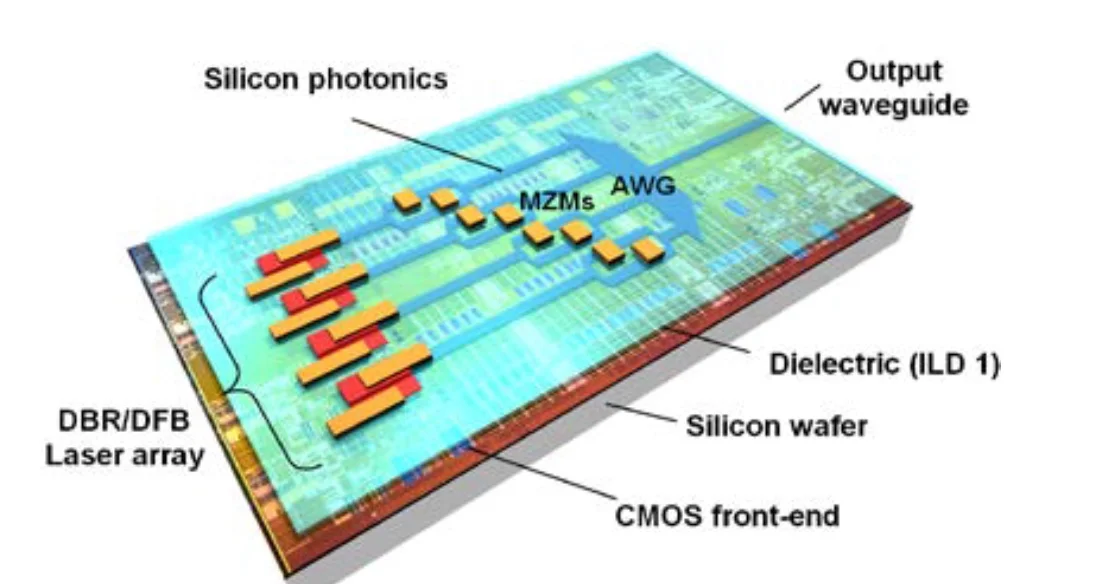 The Dimension process showing the passive photonics, dielectric material, BiCMOS circuitry, and the on-chip lasers and modulators. The indium phosphide material is shown in red. Source: Dimension.
Goal
Silicon photonics has long been seen as a technology having the potential to deliver optical devices at CMOS manufacturing costs. But silicon's key shortfall is that it does not lase. “What we see with today’s solutions is a very low-cost chip with a lot of functionality, which is a great thing, but in addition you need lasers,” says Bert Offrein, principal research staff member and manager of neuromorphic devices and systems at IBM Research, a participant in the Dimension project.
The laser accounts for a relatively large fraction of the total bill of materials of a silicon photonics chip. In turn, connecting the light source to the chip is not trivial and adds to the packaging costs. “In this project, we try to tackle this [laser] issue,” says Offrein.
The project's goal is to develop manufacturing processes that will enable the integration of photonics, including the laser, and electronics, all on one chip. “By fully integrating the laser on the chip, we massively reduce the cost and create additional functionality,” says Offrein.
“This is the true embodiment of what people first pictured as silicon photonics: the combination of optics and electronics on a single chip,” says Lars Zimmermann, team leader, silicon photonics at the Innovations for High Performance Microelectronics (IHP) research institute, another member of Dimension.
Proof-of-concept demonstrators
Dimension is a four-year project that will end in early 2020. Other project participants besides IBM Research and the IHP include ADVA Optical Networking, Opticap and the Athens Information Technology (AIT) research centre. The Dresden University of Technology is overseeing the project.
The project has set itself the goal of producing three proof-of-concept designs using the integrated silicon photonics technology.
One is a 400 Gigabit Ethernet (GbE) transmitter made up of eight 50 gigabit-per-second (Gbps) channels, each comprising a 25 gigabaud directly-modulated laser combined with 4-level pulse amplitude modulation (PAM4). Two variants are planned: a directly modulated version for the 400GbE 2km reach specification, and one with external modulation for the 400GbE 10km reach standard.
Another design is a coherent transmitter for such applications as data centre interconnect, compromising a monolithically integrated narrow-linewidth tunable laser, modulator and driver. The coherent transmitter will have a 10km target reach, will operate at 25Gbps and have a tunable narrow linewidth of under 1MHz.
The third, final demonstrator is a directly-modulated 25-gigabit non-return-to-zero laser using indium phosphide grown directly on the silicon.
By fully integrating the laser on the chip, we massively reduce the cost and create additional functionality
Process details
The silicon photonics manufacturing process involves using a silicon-on-insulator (SOI) wafer to implement the passive photonics functions and the electronics. The electronics supports high-speed analogue driver transistors and a 0.25-micron BiCMOS process used to implement the chip's control logic and control interfaces.
 Bert Offrein
The laser is constructed by first bonding a thin layer of indium phosphide. “It is structured in such a way that it [the III-V material] can be embedded completely in the whole CMOS processing,” says Offrein.
The indium phosphide layer, referred to as a III-V membrane, sits on a thin dielectric layer placed on the SOI wafer. The dielectric material is needed to protect the wafer from contamination by the III-V material and ensure that such a design could be manufactured in a BiCMOS foundry.
Once the thin indium phosphide layer is deposited, the laser can be constructed. The final stages, part of the chip-making back-end process, is the adding of metallisation layers that connect the laser and the electronics, and the circuits to the interface signals.
Growing lasers on silicon
Growing the indium phosphide layer directly on silicon, as will be done for the third demonstrator, is more exploratory. “We want to show there is a path forward on this III-V-on-silicon technology to reduce the cost further,” says Offrein.
 Lars Zimmermann
The challenge growing indium phosphide on silicon is the lattice mismatch that occurs between the two materials which leads to defects.
To tackle the issue, an approach known as confined growth is used. A small ‘seed’ is put on the silicon to act as a growth point for the indium phosphide. A small cavity is created using silica to confine the resulting growth. “The material grows in this glass cavity and the defects grow out and disappear at the edges,” says Offrein. “You then have a very high-quality III-V in this glass and this is the starting point to continue to build the quantum wells that we need.”
One challenge is enlarging the confined growth area. So far, such growth is limited to a micron whereas the length of a laser can be 500 microns typically. And once the laser is built, there remain the issues of laser reliability and temperature stability. “We will see challenges but we are not there yet,” says Offrein.
This is the true embodiment of what people first pictured as silicon photonics: the combination of optics and electronics on a single chip
Status
Dimension is tackling designs for communications but such on-chip lasers will also be useful for a range of applications such as optical sensing, says Offrein.
The project is coming to the end of its first year. Its members are creating the basic building blocks needed to realise the lasers on the silicon wafer. IBM has demonstrated the basic functionality by bonding indium phosphide to its own passive silicon photonics technology. “We have also realised the first lasers - not yet electrically pumped but optically pumped,” says Offrein. The performance of these lasers is now being characterised.
All the processes needed to pump the lasers electrically are now in place and the goal is to build complete laser structures by March 2017.
IBM is also working with IHP to see what is required to implement the technology using IHP’s own silicon photonics process. IHP is currently testing IBM’s wafers regarding any contamination issues before testing the integration process.
ADVA Optical Networking would not be on board if they were not expecting eventually to have such technology available for their products
Exploitation
The European Commission has a long history of programmes backing leading-edge research. However, Europe's track record of exploiting such research to achieve market-leading companies and products has been limited.
The European Commission staff involved in planning the Horizon 2020 projects have been far more active in ensuring that these projects are exploited, says Zimmermann. "ADVA Optical Networking would not be on board if they were not expecting eventually to have such technology available for their products," he adds.
If Dimension proves successful, IHP could make available the integrated silicon photonics process to companies to implement their opto-electronic integrated circuit designs.
IBM, while no longer a semiconductor manufacturer, would also be keen for the technology to be transferred to large foundries such as STMicroelectronics and GlobalFoundries. “That way we could purchase the technology and apply it in our own systems,” says Offrein.
Article amended on Nov 29th. Added details about the proof-of-concept demonstrators.
COBO looks inside and beyond the data centre
The Consortium of On-Board Optics is working on 400 gigabit optics for the data centre and also for longer-distance links. COBO is a Microsoft-led initiative tasked with standardising a form factor for embedded optics.
Established in March 2015, the consortium already has over 50 members and expects to have early specifications next year and first hardware by late 2017.
 Brad Booth
Brad Booth, the chair of COBO and principal architect for Microsoft’s Azure Global Networking Services, says Microsoft plans to deploy 100 gigabit in its data centres next year and that when the company started looking at 400 gigabit, it became concerned about the size of the proposed pluggable modules, and the interface speeds needed between the switch silicon and the pluggable module.
“What jumped out at us is that we might be running into an issue here,” says Booth.
This led Microsoft to create the COBO industry consortium to look at moving optics onto the line card and away from the equipment’s face plate. Such embedded designs are already being used for high-performance computing, says Booth, while data centre switch vendors have done development work using the technology.
On-board optics delivers higher interface densities, and in many cases in the data centre, a pluggable module isn’t required. “We generally know the type of interconnect we are using, it is pretty structured,” says Booth. But the issue with on-board optics is that existing designs are proprietary; no standardised form factor exists.
“It occurred to us that maybe this is the problem that needs to be solved to create better equipment,” says Booth. Can the power consumed between switch silicon and the module be reduced? And can the interface be simplified by eliminating components such as re-timers?
“This is worth doing if you believe that in the long run - not the next five years, but maybe ten years out - optics needs to be really close to the chip, or potentially on-chip,” says Booth.
400 gigabit
COBO sees 400 gigabit as a crunch point. For 100 gigabit interconnect, the market is already well served by various standards and multi-source agreements so it makes no sense for COBO to go head-to-head here. But should COBO prove successful at 400 gigabit, Booth envisages the specification also being used for 100, 50, 25 and even 10 gigabit links, as well as future speeds beyond 400 gigabit.
The consortium is developing standardised footprints for the on-board optics. “If I want to deploy 100 gigabit, that footprint will be common no matter what the reach you are achieving with it,” says Booth. “And if I want a 400 gigabit module, it may be a slightly larger footprint because it has more pins but all the 400 gigabit modules would have a similar footprint.”
COBO plans to use existing interfaces defined by the industry. “We are also looking at other IEEE standards for optical interfaces and various multi-source agreements as necessary,” says Booth. COBO is also technology agnostic; companies will decide which technologies they use to implement the embedded optics for the different speeds and reaches.
“This is worth doing if you believe that in the long run - not the next five years, but maybe ten years out - optics needs to be really close to the chip, or potentially on-chip."
Reliability
Another issue the consortium is focussing on the reliability of on-board optics and whether to use socketed optics or solder the module onto the board. This is an important consideration given that is it is the vendor’s responsibility to fix or replace a card should a module fail.
This has led COBO to analyse the causes of module failure. Largely, it is not the optics but the connections that are the cause. It can be poor alignment with the electrical connector or the cleanliness of the optical connection, whether a pigtail or the connectors linking the embedded module to the face plate. “The discussions are getting to the point where the system reliability is at a level that you have with pluggables, if not better,” says Booth.
Dropping below $1-per-gigabit
COBO expects the cost of its optical interconnect to go below the $1-per-gigabit industry target. “The group will focus on 400 gigabit with the perception that the module could be four modules on 100 gigabit in the same footprint,” says Booth. Using four 100 gigabit optics in one module saves on packaging and the printed circuit board traces needed.
Booth says that 100 gigabit optics is currently priced between $2 and $3-per-gigabit. “If I integrate that into a 400 gigabit module, the price-per-gig comes down significantly” says Booth. “All the stuff I had to replicate four times suddenly is integrated into one, cutting costs significantly in a number of areas.” Significantly enough to dip below the $1-per-gigabit, he says.
Power consumption and line-side optics
COBO has not specified power targets for the embedded optics in part because it has greater control of the thermal environment compared to a pluggable module where the optics is encased in a cage. “By working in the vertical dimension, we can get creative in how we build the heatsink,” says Booth. “We can use the same footprint no matter whether it is 100 gigabit inside or 100 gigabit outside the data centre, the only difference is I’ve got different thermal classifications, a different way to dissipate that power.”
The consortium is investigating whether its embedded optics can support 100 gigabit long-haul optics, given such optics has traditionally been implemented as an embedded design. “Bringing COBO back to that market is extremely powerful because you can better manage the thermal environment,” says Booth. And by removing the power-hungry modules away from the face plate, surface area is freed up that can be used for venting and improving air flow.
“We should be considering everything is possible, although we may not write the specification on Day One,” says Booth. “I’m hoping we may eventually be able to place coherent devices right next to the COBO module or potentially the optics and the coherent device built together.
“If you look at the hyper-scale data centre players, we have guys that focus just as much on inside the data centre as they do on how to connect the data centres in within a metro area, national area and then sub-sea,” says Booth. “That is having an impact because when we start looking at what we want to do with those networks, we want to have some level of control on what we are doing there and on the cost.
“We buy gazillions of optical modules for inside the data centre. Why is it that we have to pay exorbitant prices for the ones that we are not using inside [the data centre],” he says.
“I can’t help paint a more rosier picture because when you have got 1.4 million servers, if I end up with optics down to all of those, that is a lot of interconnect“
Market opportunities
Having a common form factor for on-board optics will allow vendors to focus on what they do best: the optics. “We are buying you for the optics, we are not buying you for the footprint you have on the board,” he says.
Booth is sensitive to the reservations of optical component makers to such internet business-led initiatives. “It is a very tough for these guys to extend themselves to do this type of work because they are putting a lot of their own IP on the line,” says Booth. “This is a very competitive space.”
But he stresses it is also fiercely competitive between the large internet businesses building data centres. “Let’s sit down and figure out what does it take to progress this industry. What does it take to make optics go everywhere?”
Booth also stresses the promising market opportunities COBO can serve such as server interconnect.
“When I look at this market, we are talking about doing optics down to our servers,” says Booth. “I can’t help paint a more rosier picture because when you have got 1.4 million servers, if I end up with optics down to all of those, that is a lot of interconnect.“
ECOC 2015 Review - Part 1
- Several companies announced components for 400 gigabit optical transmission
- NEL announced a 200 gigabit coherent DSP-ASIC
- Lumentum ramps production of its ROADM blades while extending the operating temperature of its tunable SFP+
400 gigabit
Oclaro, Teraxion and NeoPhotonics detailed their latest optical components for 400 gigabit optical transmission using coherent detection.
Oclaro and Teraxion announced 400 gigabit modulators for line-side transmission; Oclaro’s based on lithium niobate and Teraxion’s an indium phosphide one.
NeoPhotonics outlined other components that will be required for higher-speed transmission: indium phosphide-based waveguide photo-detectors for coherent receivers, and ultra-narrow line-width lasers suited for higher order modulation schemes such as dual-polarisation 16-quadrature amplitude modulation (DP-16-QAM) and DP-64-QAM.
There are two common approaches to achieve higher line rates: higher-order modulation schemes such as 16-QAM and 64-QAM, and optics capable of operating at higher signalling rates.
Using 16-QAM doubles the data rate compared to quadrature phase-shift keying (QPSK) modulation that is used at 100 Gig, while 64-QAM doubles the data rate again to 400 gigabit.
Higher-order modulation can use 100 gigabit optics but requires additional signal processing to recover the received data that is inherently closer together. “What this translates to is shorter reaches,” says Ferris Lipscomb, vice president of marketing at NeoPhotonics.
These shorter distances can serve data centre interconnect and metro applications where distances range from sub-100 kilometers to several hundred kilometers. But such schemes do not work for long haul where sensitivity to noise is too great, says Lipscomb.
What we are seeing from our customers and from carriers looking at next-generation wavelength-division multiplexing systems for long haul is that they are starting to design their systems and are getting ready for 400 Gig
Lipscomb highlights the company’s dual integrable tunable laser assembly (iTLAs) with its 50kHz narrow line-width. “That becomes very important for higher-order modulation because the different states are closer together; any phase noise can really hurt the optical signal-to-noise ratio,” he says
The second approach to boost transmission speed is to increase the signalling rate. “Instead of each stream at 32 gigabaud, the next phase will be 42 or 64 gigabaud and we have receivers that can handle those speeds,” says Lipscomb. The use of 42 gigabaud can be seen as an intermediate step to a higher line rate - 300 gigabit – while being less demanding on the optics and electronics than a doubling to 64 gigabaud.
Oclaro’s lithium niobate modulator supports 64 gigabaud. “We have increased the bandwidth beyond 35 GHz with a good spectral response – we don’t have ripples – and we have increased the modulator’s extinction ratio which is important at 16-QAM,” says Robert Blum, Oclaro’s director of strategic marketing.
We have already demonstrated a 400 Gig single-wavelength transmission over 500km using DP-16-QAM and 56 gigabaud
Indium phosphide is now coming to market and will eventually replace lithium niobate because of the advantages of cost and size, says Blum, but lithium niobate continues to lead the way for highest speed, long-reach applications. Oclaro has been delivering its lithium niobate modulator since the third quarter of the year.
Teraxion offers an indium phosphide modulator suited to 400 gigabit. “One of the key differentiators of our modulator is that we have a very high bandwidth such that single-wavelength transmission at 400 Gig is possible,” says Martin Guy, CTO and strategic marketing at Teraxion. “We have already demonstrated a 400 Gig single-wavelength transmission over 500km using DP-16-QAM and 56 gigabaud.”
“What we are seeing from our customers and from carriers looking at next-generation wavelength-division multiplexing systems for long haul is that they are starting to design their systems and are getting ready for 400 Gig,” says Blum.
Teraxion says it is seeing a lot of activity regarding single-wavelength 400 Gig transmission. “We have sampled product to many customers,” says Guy.
NeoPhotonics says the move to higher baud rates is still some way off with regard systems shipments, but that is what people are pursuing for long haul and metro regional.
200 Gig DSP-ASIC
Another key component that will be needed for systems operating at higher transmission speeds is more powerful coherent digital signal processors (DSPs). NTT Electronics (NEL) announced at ECOC that it is now shipping samples of its 200 gigabit DSP-ASIC, implemented using a 20nm CMOS process.
Dubbed the NLD0660, the DSP features a new core that uses soft-decision forward error correction (SD-FEC) that achieves a 12dB net coding gain. Improving the coding gain allows greater spans before optical regeneration or longer overall reach, says NEL. The DSP-ASIC supports several modulation formats: DP-QPSK, DP-8-QAM and DP-16-QAM, for 100 Gig, 150 Gig and 200 Gig rates, respectively. Using two NLD0660s, 400 gigabit coherent transmission is achieved.
NEL announced its first 20nm DSP-ASIC, the lower-power 100 gigabit NLD0640 at OFC 2015 in March. At the same event, ClariPhy demonstrated its own merchant 200 gigabit DSP-ASIC.
Reconfigurable optical add/ drop multiplexers
Lumentum gave an update on its TrueFlex route & select architecture Super Transport Blade, saying it has now been qualified, with custom versions of the line card being manufactured for equipment makers. The Super Transport Blades will be used in next-generation ROADMs for 100 gigabit metro deployments. The Super Transport Blade supports flexible grid, colourless, directionless and contentionless ROADM designs.
“This is the release of the full ROADM degree for next-generation networks, all in a one-slot line card,” says Brandon Collings, CTO of Lumentum. “It is a pretty big milestone; we have been talking about it for years.”
Collings says that the cards are customised to meet an equipment maker’s particular requirements. “But they are generally similar in their core configuration; they all use twin wavelength-selective switches (WSSes), those sort of building blocks.”
This is the release of the full ROADM degree for next-generation networks, all in a one-slot line card. It is a pretty big milestone; we have been talking about it for years
Lumentum also announced 4x4 and 6x6 integrated isolator arrays. “If you look at those ROADMs, there is a huge number of connections inside,” says Collings. The WSSes can be 1x20 and two can be used - a large number of fibres - and at certain points isolators are required. “Using discrete isolators and needing a large number, it becomes quite cumbersome and costly, so we developed a way to connect four or six isolators in a single package,” he says.
A 6x6 isolator array is a six-lane device with six hardwired input/ output pairs, with each input/ output pair having an isolator between them. “It sounds trivial but when you get to that scale, it is truly enabling,” says Collings.
Isolators are needed to keep light from going in the wrong direction. “These things can start to accumulate and can be disruptive just because of the sheer volume of connections that are present,” says Collings.
Tunable transceivers
Lumentum offers a tunable SFP+ module that consumes less than 1.5W while operating over a temperature range of -5C to +70C. At ECOC, the company announced that in early 2016 it will release a tunable SFP+ with an extended temperature range of -5C to +85C.
Further information
Heading off the capacity crunch, click here
For the ECOC Review, Part 1, click here
OIF moves to raise coherent transmission baud rate
"We want the two projects to look at those trade-offs and look at how we could build the particular components that could support higher individual channel rates,” says Karl Gass of Qorvo and the OIF physical and link layer working group vice chair, optical.
 Karl Gass
The OIF members, which include operators, internet content providers, equipment makers, and optical component and chip players, want components that work over a wide bandwidth, says Gass. This will allow the modulator and receiver to be optimised for the new higher baud rate.
“Perhaps I tune it [the modulator] for 40 Gbaud and it works very linearly there, but because of the trade-off I make, it doesn’t work very well anywhere else,” says Gass. “But I’m willing to make the trade-off to get to that speed.” Gass uses 40 Gbaud as an example only, stressing that much work is required before the OIF members choose the next baud rate.
"We want the two projects to look at those trade-offs and look at how we could build the particular components that could support higher individual channel rates”
The modulator and receiver optimisations will also be chosen independent of technology since lithium niobate, indium phosphide and silicon photonics are all used for coherent modulation.
The OIF has not detailed timescales but Gass says projects usually take 18 months to two years.
Meanwhile, the OIF has completed two projects, the specification outputs of which are referred to as implementation agreements (IAs).
One is for integrated dual polarisation micro-intradyne coherent receivers (micro-ICR) for the CFP2. At OFC 2015, several companies detailed first designs for coherent line side optics using the CFP2 module.
The second completed IA is the 4x5-inch second-generation 100 Gig long-haul DWDM transmission module.
NeoPhotonics to expand its tunable laser portfolio
Part 1: Tunable lasers
NeoPhotonics will become the industry's main supplier of narrow line-width tunable lasers for high-speed coherent systems once its US $17.5 million acquisition of Emcore's tunable laser business is completed. Gazettabyte spoke with Ferris Lipscomb of NeoPhotonics about Emcore's external cavity laser and the laser performance attributes needed for metro and long haul.
 Key specifications and attributes of Emcore's external cavity laser and NeoPhotonics's DFB laser array. Source: NeoPhotonics.
Emcore and NeoPhotonics are leading suppliers of tunable lasers for the 100 Gigabit coherent market, according to market research firm Ovum. NeoPhotonics will gain Emcore's external cavity laser (ECL) on the completion of the deal, expected in January. The company will also gain Emcore's integrable tunable laser assembly (ITLA), micro ITLA, tunable XFP transceiver, tunable optical sub-assemblies, and 10, 40, 100 and 400 Gig integrated coherent transmitter products.
Emcore's ECL has a long history. Emcore acquired the laser when it bought Intel's optical platform division for $85 million in 2007, while Intel acquired the laser from New Focus in 2002 in a $50 million deal. Meanwhile, NeoPhotonics bought Santur's distributed feedback (DFB) tunable laser array in 2011 in a $39 million deal.
The two lasers satisfy different needs: Emcore's is suited for high-speed long distance transmission while NeoPhotonics's benefits metro and intermediate distances.
The Emcore laser uses mirrors and optics external to the gain medium to create the laser's relatively long cavity. This aids high-performance coherent systems as it results in a laser with a narrow line-width. Coherent detection uses a mixing technique borrowed from radio where an incoming signal is recovered by compared it with a local oscillator or tone. "The narrower the line-width, the more pure that tone is that you are comparing it to," says Lipscomb.
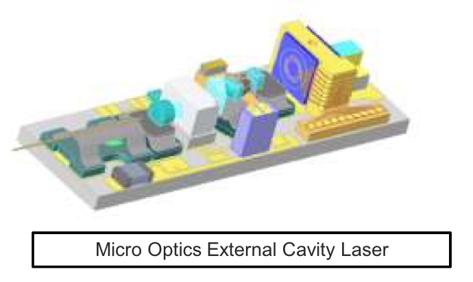 Source: NeoPhotonics
A narrower line-width also means less digital signal processing (DSP) is needed to resolve the ambiguity that results from that line-width, says Lipscomb: "And the more DSP power can be spent on either compensating fibre impairments or going further [distances], or compensating the higher-order modulation schemes which require more DSP power to disentangle."
The ECL has a narrow line-width that is specified at under 100kHz. "It is probably closer to 20kHz," says Lipscomb. One of the laser's drawbacks is that its uses a mechanical tuning mechanism that is relatively slow. It also has a lower output power of 16dBm compared to NeoPhotonics's DFB laser array that is up to 18dBm.
The metro market for 100 Gig coherent will emerge in volume towards the end of 2015 or early 2016
In contrast, NeoPhotonics' DFB laser array, suited to metro and intermediate reach applications, has a wider line-width specified at 300kHz, although 200kHz is typical. The DFB design comprises multiple lasers integrated compactly. The laser design also uses a MEMS that results in efficient coupling and the higher - 18dBm - output power. "Using the MEMS structure, you can integrate the laser with other indium phosphide or silicon photonics devices," says Lipscomb. "That is a little bit harder to do with the Emcore device."
 Source: NeoPhotonics
It is the compactness and higher power of the DFB laser array that makes it suited to metro networks. The higher output power means that one laser can be used for both transmission and the local oscillator used to recover the received coherent signal. "More power can be good if you can live with the broader line-width," says Lipscomb. "It reduces overall system cost and can support higher-order modulation schemes over shorter distances."
Market opportunities
NeoPhotonics' focus is on narrow line-width lasers for coherent systems operating at 100 Gigabit and greater speeds. Lipscomb says the metro market for 100 Gig coherent will emerge in volume towards the end of 2015 or early 2016. "The distance here is less and therefore less compensation is needed and a little bit more line-width is tolerable," he says. "Also cost is an issue and a more integrated product can have potentially a lower cost."
For long haul, and especially at transmission rates of 200 and 400 Gig, the demands placed on the DSP are considerable. This is where Emcore's laser, with is narrow line-width, is most suited.
System vendors are already investigating 400 Gig and above transmission speeds. "For the high-end, line-width is going to be a critical factor," says Lipscomb. "Whatever modulation schemes there are to do the higher speeds, they are going to be the most demanding of laser performance."
For Part 2: Is the tunable laser market set for an upturn? click here
Acacia uses silicon photonics for its 100G coherent CFP
Acacia Communications has revealed the innards of its 100 Gig coherent pluggable module for metro networks. The AC-100 CFP combines a low-power DSP-ASIC with a silicon-photonics-based optics chip. The CFP's reach is 80km to 1,200km, and its power consumption is 24-26W, well within the pluggable's maximum power profile of 32W.
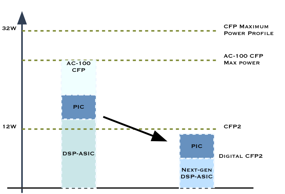 The power consumption of the AC-100 CFP, and its main components, and the target power consumptions of the components needed for a digital CFP2. Source: Gazettabyte
The start-up says it is shipping samples of the AC-100 CFP and already has 15 customers. "That includes some of the bigger [systems] players that have their own internal DSP," says Raj Shanmugaraj, CEO of Acacia. "The coherent CFP is not their focus; they are going after long-haul."
The start-up is shipping samples of the AC-100 CFP and already has 15 customers
Acacia chose to develop it own DSP chips as it sees the technology as core for coherent-based optical transmission. "That is where we see the big market," says Shanmugaraj. "We have a 100 Gig [MSA] that has been shipping, and a 200-400 Gig product that is in development."
DSP-ASIC and silicon photonics
The DSP-ASIC for the AC-100 CFP is Acacia's second chip design. Its first, a DSP-ASIC for its long-haul 5x7-inch OIF MSA transponder, is implemented using a 40nm CMOS process. The latest metro DSP-ASIC uses 28nm CMOS.
The DSP-ASIC includes analogue-to-digital (A/D) and digital-to-analogue (D/A) converters and a serialiser/ deserialiser (Serdes). Also on-chip is the digital signal processor (DSP) that implements soft-decision, forward error correction (SD-FEC) and compensation algorithms for chromatic and polarisation-mode dispersion.
Other DSP-ASIC features include spectral shaping for flexible grid transmission. "The signal processing on the transmit side fits in the one ASIC," says Benny Mikkelsen, CTO at Acacia. Also on-chip are a 100 Gig OTN (Optical Transport Network) framer and a microprocessor to manage the DSP-ASIC and the overall CFP.
The DSP-ASIC consumes 12-14W: the A/D, D/A converters and Serdes consume 5W, while the DSP consumes 7W for an 80km link - the 100 Gig equivalent of the -ZR spec - and 9W for 1,200km transmission due to the more powerful SD-FEC needed.
Mikkelsen says achieving a low-power ASIC requires several approaches. The SD-FEC is designed to be extremely low power, he says, as is the dispersion compensation: "Not just the algorithms but how we code the algorithms." Also, how the ASIC's circuitry is laid out impacts power consumption.
Acacia's engineers have also developed a silicon-photonics chip that combines the coherent transmitter and receiver optics. "The PIC [photonic integrated circuit] is the first silicon-photonics chip targeted at metro/ metro-regional," says Shanmugaraj. "It is an IC that has all the components except the laser, and is co-packaged in a gold box with the drivers and trans-impedance amplifiers."
Acacia's PIC is monolithic; all the functional blocks are implemented in silicon rather than combined silicon and III-V materials, a technique known as heterogeneous integration.
Using silicon photonics rather than indium phosphide has advantages, says Shanmugaraj. Silicon photonics benefits from mature CMOS processes developed for the semiconductor industry: "With the large silicon wafers, you can have thousands of these silicon PICs on them," he says.
Acacia tests the PICs directly on the wafer. This avoids having to dice the wafer and package each die before testing. "We also don't need thermal control [of the chip] or hermetic packaging," says Shanmugaraj. With indium phosphide, the modulators do require thermal cooling, adding to the design complexity and the power consumption. The PIC is 10mm long and consumes less than 5W.

The AC-100 CFP is expected to cost less than half the 5x7-inch 100 Gig coherent MSA which sells for $20,000. "One of the biggest pain points in metro is cost, if you ask most of the service providers," says Shanmugaraj. At below $10,000, the coherent CFP will be cost-competitive with the 100 Gig direct-detection CFP that uses 4x25 Gig wavelengths. However, the 100 Gig direct-detection CFP continues to come down in price as more products come to market.
Roadmap
Acacia will continue to address long-haul and metro, each requiring its own ASIC. "We don't believe that you can have one ASIC that serves both submarine and the metro," says Mikkelsen. In turn, silicon photonics will be used for pluggables while discrete optics will be used for the more demanding submarine.
The company says it is developing a multi-core ASIC to support super-channels and 16-QAM modulation for 200 Gig and 400 Gig transmission. The company says it will provide more details of its flexible, adaptive-rate ASIC at ECOC, to be held in September this year.
The company's product roadmap also features a co-packaged DSP-ASIC and PIC that will fit within a CFP2. Achieving such a pluggable, dubbed a digital CFP2, require a further halving of the DSP-ASIC's power consumption. This, says Acacia, is achievable using the next CMOS process node after 28nm.
The advantages of a digital CFP2 compared to a CFP2 with optics only, with the DSP-ASIC on the line card, include using the DSP-ASIC only when it is needed. When a fault occurs, the relevant pluggable can be replaced rather than having to remove the complete line card. Lastly, new functionality in the DSP-ASIC can be introduced by plugging in the new CFP2 pluggable compared with having to redesign the line card.
See also:
Transmode adopts 100 Gigabit coherent CFPs, click here
ClariPhy samples a 200 Gigabit coherent DSP-ASIC, click here
ECI Telecom demos 100 Gigabit over 4,600km
- 4,600km optical transmission over submarine cable
- The Tera Santa Consortium, chaired by ECI, will show a 400 Gigabit/ 1 Terabit transceiver prototype in the summer
- 100 Gigabit direct-detection module on hold as the company eyes new technology developments
 "When we started the project it was not clear whether the market would go for 400 Gig or 1 Terabit. Now it seems that the market will start with 400 Gig."
Jimmy Mizrahi, ECI Telecom
ECI Telecom has transmitted a 100 Gigabit signal over 4,600km without signal regeneration. Using Bezeq International's submarine cable between Israel and Italy, ECI sent the 100 Gigabit-per-second (Gbps) signal alongside live traffic. The Apollo optimised multi-layer transport (OMLT) platform was used, featuring a 5x7-inch MSA 100Gbps coherent module with soft-decision, forward error correction (SD-FEC).
"We set a target for the expected [optical] performance with our [module] partner and it was developed accordingly," says Jimmy Mizrahi, head of the optical networking line of business at ECI Telecom. "The [100Gbps] transceiver has superior performance; we have heard that from operators that have tested the module's capabilities and performance."
One geography that ECI serves is the former Soviet Union which has large-span networks and regions of older fibre.
Tera Santa Consortium
ECI used the Bezeq trial to also perform tests as part of the Tera Santa Consortium project involving Israeli optical companies and universities. The project is developing a transponder capable of 400 Gigabit and 1 Terabit rates. The project is funded by seven participating firms and the Israeli Government.
"When we started the project it was not clear whether the market would go for 400 Gig or 1 Terabit,” says Mizrahi. “Now it seems that the market will start with 400 Gig."
The Tera Santa Consortium expects to demonstrate a 1 Terabit prototype in August and is looking to extend the project a further three years.
100 Gigabit direct detection
In 2012 ECI announced it was working with chip company, MultiPhy, to develop a 100 Gigabit direct-detection module. The 100 Gigabit direct detection technology uses 4x28Gbps wavelengths and is a cheaper solution than 100Gbps coherent. The technology is aimed at short reach (up to 80km) links used to connect data centres, for example, and for metro applications.
“We have changed our priorities to speed up the [100Gbps] coherent solution,” says Mizrahi. “It [100Gbps direct detection] is still planned but has a lower priority.”
ECI says it is monitoring alternative technologies coming to market in the next year. “We are taking it slowly because we might jump to new technologies,” says Mizrahi. “The line cards will be ready, the decision will be whether to go for new technologies or for direct detection."
Mizrahi would not list the technologies but hinted they may enable cheaper coherent solutions. Such coherent modules would not need SD-FEC to meet the shorter reach, metro requirements. Such a module could also be pluggable, such as the CFP or even the CFP2, and use indium phosphide-based modulators.
“For certain customers pricing will always be the major issue,” says Mizrahi. “If you have a solution at half the price, they will take it.”
Cisco Systems demonstrates 100 Gigabit technologies
* Announces 100 Gigabit transmission over 4,800km

"CPAK helps accelerate the feasibility and cost points of deploying 100Gbps"
Stephen Liu, Cisco
Cisco Sytems has announced that its 100 Gigabit coherent module has achieved a reach of 4,800km without signal regeneration. The span was achieved in the lab and the system vendor intends to verify the span in a customer's network.
The optical transmission system achieved a reach of 3,000km over low-loss fibre when first announced in 2012. The extended reach is not a result of a design upgrade, rather the 100 Gigabit-per-second (Gbps) module is being used on a link with Raman amplification.
Cisco says it started shipping its 100Gbps coherent module in June 2012. "We have shipped over 2,000 100Gbps coherent dense WDM ports," says Sultan Dawood, marketing manager at Cisco. The 100Gbps ports include line-side 100Gbps interfaces integrated within Cisco's ONS 15454 multi-service transport platform and its CRS core router supporting its IP-over-DWDM elastic core architecture.
Cisco has also coupled the ASR 9922 series router to the ONS 15454. "We are extending what we have done for IP and optical convergence in the core," says Stephen Liu, director of market management at Cisco. "There is now a common solution to the [network] edge."
None of Cisco's customers has yet used 100Gbps over a 3,000km span, never mind 4,800km. But the reach achieved is an indicator of the optical transmission performance. "The [distance] performance is really a proxy for usefulness," says Liu. "If you take that 3,000km over low-loss fibre, what that buys you is essentially a greater degree of tolerance for existing fibre in the ground."
Much industry attention is being given to the next-generation transmission speeds of 400Gbps and one Terabit. This requires support for super-channels - multi-carrier signals to transmit 400Gbps and one Terabit as well as flexible spectrum to pack the multi-carrier signals efficiently across the fibre's spectrum. But Cisco argues that faster transmission is only one part of the engineering milestones to be achieved, especially when 100Gbps deployment is still in its infancy.
To benefit 100Gbps deployments, Cisco has officially announced its own CPAK 100Gbps client-side optical transceiver after discussing the technology over the last year. "CPAK helps accelerate the feasibility and cost points of deploying 100Gbps," says Liu.
CPAK
The CPAK is Cisco' first optical transceiver using silicon photonics technology following its acquisition of LightWire. The CPAK is a compact optical transceiver to replace the larger and more power hungry 100Gbps CFP interfaces.
The CPAK is being launched at the same time as many companies are announcing CFP2 multi-source agreement (MSA) optical transceiver products. Cisco stresses that the CPAK conforms to the IEEE 100GBASE-LR4 and -SR10 100Gbps standards. Indeed at OFC/NFOEC it is demonstrating the CPAK interfacing with a CFP2.
The CPAK will be used across several Cisco platforms but the first implementation is for the ONS 15454.
The CPAK transceiver will be generally available in the summer of 2013.
Cisco Systems' intelligent light
Network optimisation continues to exercise operators and content service providers as their requirements evolve with the growth of services such as cloud computing. Cisco Systems' announced elastic core architecture aims to tackle networking efficiency and address particular service provider requirements.

“The core [network] needs to be more robust, agile and programmable”
Sultan Dawood, Cisco
“The core [network] needs to be more robust, agile and programmable – especially with the advent of cloud,” says Sultan Dawood, senior manager, service provider marketing at Cisco. “As service providers look at next-generation infrastructure, convergence of IP and optical is going to have a big play.”
Cisco's elastic core architecture combines several developments. One is the integration of Cisco's 100 Gigabit-per-second (Gbps) dense wavelength division multiplexing (DWDM) coherent transponder, first introduced on its ROADM platform, onto its router to enable IP-over-DWDM.
This is part of what Cisco calls nLight – intelligent light - which itself has three components: its 100Gbps coherent ASIC hardware, the nLight control plane and nLight colourless and contentionless ROADMs. “As packet and optical networks converge, intelligence between the layers is needed,” says Dawood. “Today how the ROADM and the router communicate is limited."
There is the GMPLS [Generalized Multi-Protocol Label Switching] layer working at the IP layer, and WSON [Wavelength Switched Optical Layer] working at the optical layer. These two protocols are doing control plane functions at each of their respective layers. "What nLight is doing is communicating between these two layers [using existing parameters] and providing the interaction," says Dawood.
Ron Kline, principal analyst for network infrastructure at Ovum, describes nLight more generally as Cisco’s strategy for software-defined networking: "Interworking control planes to share info across platforms and add the dynamic capabilities."
The second component of Cisco's announcement is an upgrade of its carrier-grade services engine, from 20Gbps to 80Gbps, that fits within Cisco's CSR-3 core router and will be available from May 2013. The services engine enables such services as IPv6 and 'cloud routing' - network positioning which determines the most suitable resource for a customer’s request based on the content’s location and the data centre's loading.
Cisco has also added anti distributed denial of service (anti-DDoS) software to counter cyber threats. “We have licensed software that we have put into our CRS-3 so that with our VPN services we can provide threat mitigation and scrub any traffic liable to hurt our customers,” says Dawood.
nLight
According to Cisco, several issues need to be addressed between the IP and optical layers. For example, how the router and the optical infrastructure exchange information like circuit ID, path identifiers and real-time information in order to avoid the manual intervention used currently.
“With this intelligent data that is extracted due to these layers communicating, I can now make better, faster decisions that result in rapid service provisioning and service delivery,” says Dawood.
Cisco cites as an example a financial customer requesting a low-latency path. In this case, the optical network comes back through this nLight extraction process and highlights the most appropriate path. That path has a circuit ID that is assigned to the customer. If the customer then comes back to request a second identical circuit, the network can make use of the existing intelligence to deliver a similar-specification circuit.
Such a framework avoids lengthy, manual interactions between the IP and transport departments of an operator required when setting up an IP VPN, for example. By exchanging data between layers, service providers can understand and improve their network topology in real-time, and be more dynamic in how they shift resources and do capacity planning in their network.
Service providers can also improve their protection and restoration schemes and also how they configure and provision services. Such capabilities will enable operators to be more efficient in the introduction and delivery of cloud and mobile services.
Total cost of ownership
Market research firm ACG Research has done a total cost of ownership (TCO) analysis of Cisco's elastic core architecture. It claims using nLight achieves up to a halving of the TCO of the optical and packet core networks in designs using protected wavelengths. It also avoids a 10% overestimation of required capacity.
Meanwhile, ACG claims an 18-month payback and 156% return on investment from a CRS CGSE service module with its anti‐DDoS service, and a 24% TCO savings from demand engineering with the improved placement of routes and cloud service workload location.
Cisco says its designed framework architecture is being promoted in the Internet Engineering Task Force (IETF). The company is also liaising with the International Telecommunication Union (ITU) and the Optical Internetworking Forum (OIF) where relevant.