OFC 2025 industry reflections - Part 2
Gazettabyte is asking industry figures for their thoughts after attending the 50th-anniversary OFC show in San Francisco. In Part 2, the contributions are from BT’s Professor Andrew Lord, Chris Cole, Coherent’s Vipul Bhatt, and Juniper Network’s Dirk van den Borne.ontent
Professor Andrew Lord, Head of Optical Network Research at BT Group
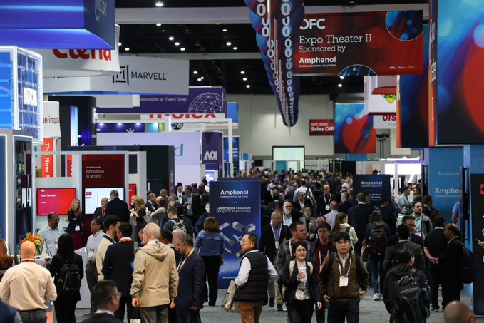
OFC was a highly successful and lively show this year, reflecting a sense of optimism in the optical comms industry. The conference was dominated by the need for optics in data centres to handle the large AI-driven demands. And it was exciting to see the conference at an all-time attendance peak.
From a carrier perspective, I continued to appreciate the maturing of 800-gigabit plugs for core networks and 100GZR plugs (including bidirectional operation for single-fibre working) for the metro-access side.
Hollow-core fibre continues to progress with multiple companies developing products, and evidence for longer lengths of fibre in manufacturing. Though dominated by data centres and low-latency applications such as financial trading, use cases are expected to spread into diverse areas such as subsea cables and 6G xHaul.
There was also a much-increased interest in fibre sensing as an additional revenue generator for telecom operators, although compelling use cases will require more cost-effective technology.
Lastly, there has been another significant increase in quantum technology at OFC. There was an ever-increasing number of Quantum Key Distribution (QKD) protocols on display but with a current focus on Continuous—Variable QKD (CV-QKD), which might be more readily manufacturable and easier to integrate.
Chris Cole, Optical Communications Advisor
For the premier optics conference, the amount of time and floor space devoted to electrical interfaces was astounding.
Even more amazing is that while copper’s death at the merciless hands of optics continues to be reported, the percentage of time devoted to electrical work at OFC is going up. Multiple speakers commented on this throughout the week.
One reason is that as rates increase, the electrical links connecting optical links to ASICs are becoming disproportionately challenging. The traditional Ethernet model of electrical adding a small penalty to the overall link is becoming less valid.
Another reason is the introduction of power-saving interfaces, such as linear and half-retimed, which tightly couple the optical and electrical budgets.
Optics engineers now have to worry about S-parameters and cross-talk of electrical connectors, vias, package balls, copper traces and others.
The biggest buzz in datacom was around co-packaged optics, helped by Nvidia’s switch announcements at GTC in March.
Established companies and start-ups were outbidding each other with claims of the highest bandwidth in the smallest space; typically the more eye-popping the claims, the less actual hard engineering data to back them up. This is for a market that is still approximately zero and faces its toughest hurdles of yield and manufacturability ahead.
To their credit, some companies are playing the long game and doing the slow, hard work to advance the field. For example, I continue to cite Broadcom for publishing extensive characterisation of their co-packaged optics and establishing the bar for what is minimally acceptable for others if they want to claim to be real.
The irony is that, in the meantime, pluggable modules are booming, and it was exciting to see so many suppliers thriving in this space, as demonstrated by the products and traffic in their booths.
The best news for pluggable module suppliers is that if co-packaged optics takes off, it will create more bandwidth demand in the data centre, driving up the need for pluggables.
I may have missed it, but no coherent ZR or other long-range co-packaged optics were announced.
A continued amazement at each OFC is the undying interest and effort in various incarnations of general optical computing.
Despite having no merit as easily shown on first principles, the number of companies and researchers in the field is growing. This is also despite the market holding steady at zero.
The superficiality of the field is best illustrated by a slogan gaining popularity and heard at OFC: computing at the speed of light. This is despite the speed of propagation being similar in copper and optical waveguides. The reported optical computing devices are hundreds of thousands or millions of times larger than equivalent CMOS circuits, resulting in the distance, not the speed, determining the compute time.
Practical optical computing precision is limited to about four bits, unverfied claims of higher precision not withstanding, making it useless in datacenter applications.
Vipul Bhatt, Vice President, Corporate Strategic Marketing at Coherent.
Three things stood out at OFC:
- The emergence of transceivers based on 200-gigabit VCSELs
- A rising entrepreneurial interest in optical circuit switching
- And an accelerated momentum towards 1.6-terabit (8×200-gigabit transceivers) alongside the push for 400-gigabit lanes due to AI-driven bandwidth expansion.
The conversations about co-packaged optics showed increasing maturity, shifting from ‘pluggable versus co-packaged optics’ to their co-existence. The consensus is now more nuanced: co-packaged optics may find its place, especially if it is socketed, while front-panel pluggables will continue to thrive.
Strikingly, talk of optical interconnects beyond 400-gigabit lanes was almost nonexistent. Even as we develop 400 gigabit-per-lane products, we should be planning the next step: either another speed leap (this industry has never disappointed) or, more likely, a shift to ‘fast-and-wide’, blurring the boundary between scale-out and scale-up by using a high radix.
Considering the fast cadence of bandwidth upgrades, the absence of such a pivotal discussion was unexpected.
Dirk van den Borne, director of system engineering at Juniper Networks
The technology singularity is defined as the merger of man and machine. However, after a week at OFC, I will venture a different definition where we call the “AI singularity” the point when we only talk about AI every waking hour and nothing else. The industry seemed close to this point at OFC 2025.
My primary interest at the show was the industry’s progress around 1.6-terabit optics, from scale-up inside the rack to data centre interconnect and long-haul using ZR/ZR+ optics. The industry here is changing and innovating at an incredible pace, driven by the vast opportunity that AI unlocks for companies across the optics ecosystem.
A highlight was the first demos of 1.6-terabit optics using a 3nm CMOS process DSP, which have started to tape out and bring the power consumption down from a scary 30W to a high but workable 25W. Well beyond the power-saving alone, this difference matters a lot in the design of high-density switches and routers.
It’s equally encouraging to see the first module demos with 200 gigabit-per-lane VCSELs and half-retimed linear-retimed optical (LRO) pluggables. Both approaches can potentially reduce the optics power consumption to 20W and below.
The 1.6-terabit ecosystem is rapidly taking shape and will be ready for prime time once 1.6-terabit switch ASICs arrive in the marketplace. There’s still a lot of buzz around linear pluggable optics (LPO) and co-packaged optics, but both don’t seem ready yet. LPO mostly appears to be a case of too little, too late. It wasn’t mature enough to be useful at 800 gigabits, and the technology will be highly challenging for 1.6 terabits.
The dream of co-packaged optics will likely have to wait for two more years, though it does seem inevitable. But with 1.6 terabit pluggable optics maturing quickly, I don’t see it having much impact in this generation.
The ZR/ZR+ coherent optics are also progressing rapidly. Here, 800-gigabit is ready, with proven interoperability between modules and DSPs using the OpenROADM probabilistic constellation shaping standard, a critical piece for interoperability in more demanding applications.
The road to 1600ZR coherent optics for data centre interconnect (DCI) is now better understood, and power consumption projections seem reasonable for 2nm DSP designs.
Unfortunately, the 1600ZR+ is more of a question mark to me, as ongoing standardisation is taking this in a different direction and, hence, a different DSP design from 1600ZR. The most exciting discussions are around “scale-up” and how optics can replace copper for intra-rack connectivity.
This is an area of great debate and speculation, with wildly differing technologies being proposed. However, the goal of around 10 petabit-per-second (Pbps) in cross-sectional bandwidth in a single rack is a terrific industry challenge, one that can spur the development of technologies that might open up new markets for optics well beyond the initial AI cluster application.

Steve Alexander's 30-Year Journey at Ciena
After three decades of shaping optical networking technology, Steve Alexander is stepping down as Ciena’s Chief Technology Officer (CTO).
His journey, from working on early optical networking systems to helping to implement AI as part of Ciena’s products, mirrors the evolution of telecommunications itself.
The farewell
“As soon as you say, ‘Hey guys, you know, there’s an end date’, certain things start moving,” says Alexander reflecting on his current transition period. “Some people want to say goodbye, others want more of your time.”
After 30 years of work, the bulk of it as CTO, Alexander is ready to reclaim his time, starting with the symbolic act of shutting down Microsoft Outlook.
“I don’t want to get up at six o’clock and look at my email and calendar to figure out my day,” he says.
His retirement plans blend the practical and the fun. The agenda includes long-delayed home projects and traveling with his wife. “My kids gave us dancing lessons for a Christmas present, that sort of thing,” he says with a smile.
Career journey
The emergence of the erbium-doped fibre amplifier shaped Alexander’s career.
The innovation sparked the US DARPA’s (Defense Advanced Research Projects Agency) interest in exploring all-optical networks, leading to a consortium of AT&T, Digital Equipment Corp., and MIT Lincoln Labs, where Alexander was making his mark.
“I did coherent in the late 80s and early 90s, way before coherent was cool,” he recalls. The consortium developed a 20-channel wavelength division multiplexing (WDM) test bed, though data rates were limited to around 1 Gigabit-per-second due to technology constraints.
“It was all research with components built by PhD students, but the benefits for the optical network were pretty clear,” he says.
The question was how to scale the technology and make it commercial.
A venture capitalist’s tip about a start-up working on optical amplifiers for cable TV led Alexander to Ciena in 1994, where he became employee number 12.
His first role was to help build the optical amplifier. “I ended up doing what effectively was the first kind of end-to-end link budget system design,” says Alexander. “The company produced its first product, took it out into the industry, and it’s been a great result since.”
The CTO role
Alexander became the CTO at Ciena at the end of the 1990s.
A CTO needs to have a technology and architecture mindset, he says, and highlights three elements in particular.
The first includes such characteristics as education and experience, curiosity, and imagination. Education is essential, but over time, it is interchangeable with experience. “They are fungible,” says Alexander.
Another aspect is curiosity, the desire to know how things work and why things are the way they are. Imagination refers to the ability to envisage something different from what it is now.
“One of the nicest things about the engineering skill set, whatever the field of engineering you’re in, is that with the right tools and team of people, once you have the idea, you can make it happen,” says Alexander.
Other aspects of the CTO’s role are talking, travelling, trouble-making, and tantrum throwing. “Trouble-making comes from the imagination and curiosity, wanting to do things maybe a little bit different than the status quo,” says Alexander.
And tantrums? “When things get really bad, and you just have to make a change, and you stomp your foot and pound the table,” says Alexander.
The third aspect a CTO needs is being in the “crow’s nest”, the structure at the top of a ship’s mast: “The guy looking out to figure out what’s coming: is it an opportunity? A threat? And how do we navigate around it,” says Alexander.
Technology and business model evolution
Alexander’s technological scope has grown over time, coinciding with the company’s expanding reach to include optical access and its Blue Planet unit.
“One of the reasons I stayed at the company for 30 years is that it has required a constant refresh,” says Alexander. “It’s a challenge because technology expands and goes faster and faster.”
His tenure saw the transformation from single-channel Sonet/ SDH to 16-channel WDM systems. But Alexander emphasizes that capacity wasn’t the only challenge.
“It’s not just delivering more capacity to more places, the business model of the service providers relies on more and more levels of intelligence to make it usable,” he says.
The gap between cloud operators’ agility and that of the traditional service providers became evident during Covid-19. “The reason we’re so interested in software and Blue Planet is changing that pretty big gap between the speed at which the cloud can operate and the speed at which the service provider can operate.”
Coherent optics
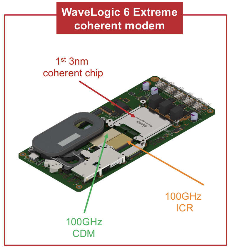
Ciena is shipping the highest symbol rate coherent modem, the WaveLogic 6 Extreme. This modem operates at up to 200 gigabaud and can send 1.6 terabits of data over a single carrier.
Alexander says coherent optics will continue to improve in terms of baud rate and optical performance. But he wonders about the desired direction the industry will take.
He marvels at the success of Ethernet whereas optical communications still has much to do in terms of standardization and interoperability.
There’s been tremendous progress by the OIF and initiatives such as 400ZR, says Alexander: “We are way better off than we were 10 years ago, but we’re still not at the point where it’s as ubiquitous and standardised as Ethernet.”
Such standardisation is key because it drives down cost.
“People have discussed getting on those Ethernet cost curves from the photonic side for years. But that is still a big hurdle in front of us,” he says.
AI’s growing impact
It is still early days for AI, says Alexander, but there are already glimmers of success. Longer term, the impact will likely be huge.
AI is already having an impact on software development and on network operations.
Ciena’s customers have started by looking to do simple things with AI, such as reconciling databases. Service providers have many such data stores: an inventory database, a customer database, a sales database, and a trouble ticket database.
“Sometimes you have a phone number here, an email there, a name elsewhere, things like a component ID, all these different things,” he says. ”If you can get all that reconciled into a consistent source of knowledge, that’s a huge benefit.”
Automation is another area that typically requires using multiple manual systems. There are also research papers appearing where AI is being used to design photonic components delivering novel optical performance.
AI will also impact the network. Humans may still be the drivers but it will be machines that do the bulk of the work and drive traffic.
“If you are going to centralize learning and distributed inferencing, it’s going to have to be closer to the end user,” says Alexander.
He uses a sports application as an example as to what could happen.
“If you’re a big soccer/ football fan, and you want to see every goal scored in every game that was broadcast anywhere in the world in the last 24 hours, ranked in a top-10 best goals listing, that’s an interesting task to give to a machine,” he says.
Such applications will demand unprecedented network capabilities. Data will need to be collected, and there will be a lot of machine-to-machine interactions to generate maybe a 10-minute video to watch.
“If you play those sorts of scenarios out, you can convince yourself that yes, networks are going to have lots of demand placed on them.”
Personal Reflection
While Alexander won’t miss his early morning Outlook checks, he’ll miss his colleagues and the laboratory environment.
A Ciena colleague, paying tribute to Alexander, describes him as being an important steward of Ciena’s culture. “He always has lived by the credo that if you care for your people, people will care for the company,” he says.
Alexander plans to keep up with technology developments, but he acknowledges that losing the inside view of innovation will be a significant change.
When people have asked him why he has stayed at Ciena, his always has answered the same way: “I joined Ciena for the technology but I stayed because of the people.”
Further Information
Ciena’s own tribute, click here

ECOC 2024 industry reflections
Gazettabyte is asking industry figures for their thoughts after attending the recent 50th-anniversary ECOC show in Frankfurt. Here are the first contributions from Huawei's Maxim Kuschnerov, Coherent's Vipul Bhatt, and Broadcom's Rajiv Pancholy.
Maxim Kuschnerov, Director R&D, Optical & Quantum Communication Laboratory at Huawei.
At ECOC, my main interest concerned the evolution of data centre networking to 400 gigabits per lane for optics and electronics. Historically, the adoption of new optical line rates always preceded the serdes electrical interconnects but now copper cables are likely to drive much of the leading development work at 400 gigabit per lane.
Arista Networks argued that 448G-PAM6 works better for copper, while 448G-PAM4 is the better choice for optics – a recurring argument. While PAM6 signalling is certainly more suitable for longer copper cables, it will face even tougher challenges on the optical side with increasing reflection requirements in newly built, dusty data centres. Also, a linear drive option for future Ethernet will be imperative, given the DSP’s increasing share of the the consumption in pluggable modules. Here, a native 448G-PAM4 format for the serdes (the attachment unit interface or AUI) and optics looks more practical.
My most important takeaway regarding components was the initial feasibility of electro-absorption modulated lasers (EMLs) with a greater than 100GHz analogue bandwidth, presented by Lumentum and Mitsubishi publicly and other companies privately. Along with thin-film lithium niobate (TFLN) Mach–Zehnder modulators suited for Direct Reach (DR) applications with shared lasers, EMLs have historically offered low cost, small size and native laser integration.
For 1.6-terabit modules, everyone is waiting on the system availability of 224-gigabit serdes at a switch and network interface card (NIC) level. The power consumption of 1.6-terabit optical modules will improve with 3nm CMOS DSPs and native 200 gigabit per lane. Still, it gets into an unhealthy region where the network cable power consumption is in the same ballpark as the system function of switching. Here, the bet on LPO certainly didn’t pay off at 100 gigabits per lane and will not pay off at 200 gigabits per lane at scale. The question is whether linear receive optics (LRO)/ half-retimed approaches will enter the market. Technically, it’s feasible. So, it might take one big market player with enough vertical integration capability and a need to reduce power consumption to move the needle into this more proprietary, closed-system direction. Nvidia showcased their PAM4 DSP at the show. Just saying…
212G VCSELs are still uncertain. There is a tight initial deployment window to be hit if these high-speed VCSELS are to displace single-mode fibre-based optics at the major operators. Coherent’s results of 34GHz bandwidth are not sufficient and don’t look like something that could yet be produced at scale. Claims by some companies that a 400 gigabit per lane VCSEL is feasible sound hollow for now, with the industry crawling around the 30GHz bandwidth window.
Last but not least, co-packaged optics. For years, this technology couldn’t escape gimmick status. Certainly, reliability, serviceability, and testability of co-packaged optics using today’s methodology would make a deployment impractical. However, the big prize at 400 gigabit per lane is saving power – a significant operational expense for operators – something that is too attractive to ignore.
The targets of improving optics diagnostics, developing higher-performance dust-reflection DSP algorithms to deal with multi-path interference, adopting more resiliency to failure in the network, and introducing a higher degree of laser sparing are not insurmountable tasks if the industry sets its mind to them. Given the ludicrous goals of the AI industry, which is reactivating and rebranding nuclear power plants, a significant reduction in network power might finally serve a higher purpose than just building a plumber’s pipe.
Vipul Bhatt, Vice President of Marketing, Datacom Vertical, Coherent
ECOC 2024 was the most convincing testimony that the optical transceiver industry has risen to the challenge of AI’s explosive growth. There was hype, but I saw more solid work than hype. I saw demonstrations and presentations affirming that the 800-gigabit generation was maturing quickly, while preparations are underway for the next leap to 1.6 terabit and then 3.2 terabit.
This is no small feat, because the optics for AI is more demanding in three ways. I call them the three P’s of AI optics: performance, proliferation, and pace.
Performance because 200 gigabit PAM4 optical lanes must work with a low error rate at higher bandwidth. Proliferation because the drive to reduce power consumption has added new transceiver variants like linear packaged optics (LPO) and linear receive optics (LRO). And pace because the specifications of AI optics are evolving at a faster pace than traditional IEEE standards.
Rajiv Pancholy, Director of Hyperscale Strategy and Products, Optical Systems Division, Broadcom
As generative AI systems move to unsupervised, transformer-based parallel architectures, there is less time for resending packets due to data transmission errors. Improved bit error rates are thus required to reduce training times while higher interconnect bandwidth and data rates are needed to support larger GPU clusters. These compute networks are already moving to 224 gigabit PAM4 well before the previous generation at 112 gigabit PAM4 was allowed to reach hyperscale deployment volumes.
The problem is scalability with a high-radix supporting all-to-all connectivity. The power for a single rack of 72 GPUs is 120kW, and even with liquid cooling, this becomes challenging. Interconnecting larger scale-up and scale-out AI computing clusters requires more switching layers which increases latency.
Furthermore, after 224 gigabit PAM4, the losses through copper at 448 gigabit PAM4 make link distances from the ASIC too short. Moving to modulation schemes like PAM-6 or PAM-8 presents a problem for the optics, which would need to stay at 448 gigabit PAM4 to minimize crosstalk and insertion losses.
Supporting 448 gigabit PAM4 with optics then potentially requires new materials to be integrated into silicon, like thin-film lithium niobate (TFLN) and Barium Titanate (BaTiO3), electro-optic (EO) polymers, and III-V materials like Indium Phosphate (InP) and Gallium Arsenide (GaAs). So now we have a gearbox and, potentially, a higher forward error correction (FEC) coding gain is required, adding more power and latency before the signal even gets to the transmit-side optics.
There were 1.6-terabit OSFP transceivers operating with eight lanes of 212.5 gigabit PAM4 while vendors continue to work towards a 3.2-terabit OSFP-XD. With 32 x 3.2Tbps pluggables operating at 40W each, the optical interconnect power would be 1.3kW for a 102.4Tbps switch. And if you use 64 x 1.6Tbps OSFP at 25W each, the optical interconnect power will be eben higher, at 1.6kW. I wonder how linear pluggable optics can compensate for all the path impairments and reflections at high data rates from pluggable solutions. Perhaps you can relax link budgets, temperature requirements, and interoperability compliance.
The best session this year was the last ECOC Market Focus panel on the Tuesday, which kept everyone a bit longer before they could figure out where in Frankfurt Oktoberfest beer was on tap. The panel addressed “Next-Gen Networking Optics like 1.6T or 3.2T”. All but one of the participants discussed the need and a migration to co-packaged optics, which we at Broadcom first demonstrated in March 2022.
It was great to also present at the ECOC Market Focus forum. My presentation was titled “Will you need CPO in 3 years?” Last year in Glasgow, I gave a similar presentation: “Will you need CPO in 5 years?”

OFC 2024 industry reflections: Part 4
Gazettabyte is asking industry figures for their thoughts after attending the recent OFC show in San Diego. This penultimate part includes the thoughts of Cisco’s Ron Horan, Coherent’s Dr. Sanjai Parthasarathi, and Adtran’s Jörg-Peter Elbers.

Ron Horan, Vice President Product Management, Client Optics Group, Cisco
Several years ago, no one could have predicted how extensive the network infrastructure required to support artificial intelligence (AI) and machine learning (ML) back-end networks in data centres would be. This year’s OFC answered that question. In a word, immense.
By 2025, the optics total addressable market for AI/ML back-end networks is expected to equal the already substantial front-end network optics market. By 2027, the back-end network optics total addressable market is projected to significantly exceed that of the front-end network. Additionally, the adoption of higher speeds and interface densities in the AI/ML back-end network will likely surpass that of the front-end.
Last year, linear pluggable optics (LPO) advocates heralded the power and cost savings associated with removing the digital signal processor (DSP) from an optics module and driving it directly from the host ASIC. Cisco and others have shown, using data and demos, that the overall power and cost savings are significant. However, in the last year, enthusiasm for this disruptive technology has been checked as concerns about link robustness and accountability have surfaced.
Enter linear receive optics (LRO), where the transmit path gets retimed while the high-power module receiver path moves to a linear receiver, which drives directly to the host ASIC. While not as power or cost friendly as linear pluggable optics, it does reduce power and some cost from the module compared to a fully retimed module while providing some diagnostic support for the link.
Only time and significant interoperability testing will determine whether linear pluggable optics or linear receive links will be robust enough to make them deployable at scale. Additionally, today’s linear pluggable and linear receive solutions have only been shown at 100 gigabits per lane. It is unclear whether 200 gigabits per lane for both approaches can work. Many think not. If not, then 100 gigabit per lane linear pluggable and linear receive optics may be a one-generation technology that is never optimal. The LPO-MSA, an industry effort that included many of the industry’s key companies, was announced before OFC to specify and resolve interoperability and link accountability concerns.
The overall concern about reducing power in the data centre was a strong theme at the show. The linear pluggable optics/ linear receive optics theme was born from this concern. As optics, switches, routers, and GPU servers become faster and denser, data centres cannot support the insatiable need for more power.
However, end users and equipment manufacturers seek alternative ways to lower power, such as liquid cooling and immersion. Liquid cooling uses liquid-filled pipes to remove the heat, which can help cool the optics. Liquid immersion further amplifies the cooling approach by immersing the optics, along with the host switch or GPU server, directly into an inert cooling fluid or placing them just above the fluid in the vapour layer. The ultimate result is to operate the optics at a lower case temperature and save power. It seems each customer is approaching this problem differently.
Last year’s OFC produced the first optics with 200 gigabit per optical lane technology. These solutions assumed a gearbox to a host interface that used 100-gigabit electrical channels. While some early adopters will use systems and optics with this configuration, a more optimal solution using 200 gigabits per lane electrical channels between the host and optics will likely be where we see 200 gigabits per lane optics hit their stride. This year’s show revealed a broader set of optics at 200 gigabit per lane rates. The technology maturity was markedly improved from last year’s early feasibility demos.
This is an exciting time in the optics industry. I look forward to learning what technologies will be introduced at OFC 2025.
Dr. Sanjai Parthasarathi, Chief Marketing Officer, Coherent
The progress in making 200-gigabit VCSELs ready for 200-gigabit PAM-4 optical transmission was a pleasant surprise of the event.
We at Coherent presented a paper on our lithographic aperture VCSEL, while Broadcom’s presentation outlined the technical feasibility of 200-gigabit PAM4 links. While both mentioned that more work is needed, the historic success of VCSEL-based links in short-reach interconnects suggests that the arrival of 200G-capable VCSELs will significantly impact the datacom market.
The feasibility of linear pluggable optics has likely delayed the market acceptance of co-packaged optics. There seems to be widespread consensus that LPO can reduce cost and power while retaining all the advantages of pluggable transceivers – a vibrant ecosystem, deployment flexibility, and a clear distinction of link accountability.
Jörg-Peter Elbers, senior vice president, advanced technology, standards and IPR, Adtran.
At this year’s OFC, discussions were much hotter than the weather. Who would have anticipated rain, winds and chilly temperatures in an always-sunny San Diego?
AI infrastructure created the most buzz at OFC. Accelerated compute clusters for generative AI are expected to drive massive demands for high-speed interconnects inside cloud-scale data centres. Consequently, 800-gigabit, 1.6-terabit, and future 3.2-terabit pluggable optical transceivers for front-end and back-end data centre fabrics stirred a lot of interest. Progress on co-packaged optics was also exciting, yet the technology will only go into deployments where and when pluggable transceivers hit unsurmountable challenges.
Silicon Photonics, indium phosphide, thin-film lithium niobate and VCSEL-based optics compete for design slots in a very competitive intra-data centre market, leading to new partnerships across the pluggable transceiver value chain. Linear receive optics and linear transmit & receive pluggable optics offer opportunities to reduce or eliminate DSP functions where electrical signal integrity permits.
While green ICT (information and communications technology) received a lot of attention at the conference, comments at the OFC Rump Session on this topic were somewhat disenchanting: time-to-market and total-cost-of-ownership drive deployment decisions at hyperscale data centres; lower energy consumption of optics is welcome but not a sufficient driver for architectural change.
On the inter-data centre side, a range of companies announced or demonstrated 800G-ZR/ZR+ transceivers at the show. More surprising was the number of transceiver vendors – including those not traditionally active in this market domain – who have added 400G-ZR QSFP-DD transceivers to their product portfolio. This indicates that the prices of these transceivers may decline faster than anticipated.
As for the next generation, industry consensus is building up behind a single-wavelength 1.6T ZR/ZR+ ecosystem using a symbol rate of some 240 gigabaud. There was a period in which indium phosphide and silicon photonics seemed to have taken over, and LiNbO3 appeared old-fashioned. With the move to higher symbol rates, LiNbO3 – in the form of thin-film Lithium Niobate – is celebrating a comeback: “Lithium Niobate is dead – long live Lithium Niobate!”
The OIF’s largest ever interop demo impressively showed how 400G-ZR+ modules can seamlessly interoperate over long-haul distances using an open-line system optimized for best performance and user-friendly operation. Monitoring and controlling such pluggable modules in IPoWDM scenarios can create operational and organizational challenges and is the subject of ongoing debates in IETF, TIP and OIF. A lean demarcation unit device can be a pragmatic solution to overcome these challenges in the near term. In the access/aggregation domain, the interest in energy-efficient 100G-ZR solutions keeps growing.
As the related OFC workshop showed, growing is also the support for a coherent single-carrier PON solution as the next step in the PON roadmap after 50Gbps very high-speed PON (VHSP).
Overall, there was excitement and momentum at OFC, with the conference and show floor returning to pre-Covid levels.
This is a good basis for the 50th anniversary edition of ECOC, taking place in Frankfurt, Germany, on September 22-26, 2024.

A coherent roadmap for co-packaged optics
Is coherent optics how co-packaged will continue to scale? Pilot Photonics certainly thinks so.

Part 1: Co-packaged optics
Frank Smyth, CTO and founder of Pilot Photonics, believes the firm is at an important inflection point.
Known for its comb laser technology, Pilot Photonics has just been awarded a €2.5 million European Innovation Council grant to develop its light-source technology for co-packaged optics.
The Irish start-up is also moving to much larger premises and is on a recruitment drive. “Many of our projects and technologies are maturing,” says Smyth.
Company
Founded in 2011, the start-up spent its early years coupled to Dublin City University. It raised its first notable investment in 2017.
The company began by making lab instrumentation based on its optical comb laser technology which emits multiple sources of light that are frequency- and phased-locked. But a limited market caused the company to pivot, adding photonic integration to its laser know-how.
Now, the start-up has a fast-switching, narrow-linewidth tunable laser, early samples of which are being evaluated by several “tier-one” companies.
Pilot Photonics also has a narrowband indium-phosphide comb laser for optical transport applications. This will be the next product it samples.
More recently, the start-up has been developing a silicon nitride-based comb laser for a European Space Agency project. “The silicon nitride micro-resonator in the comb is a non-linear element that enables a very broad comb for highly parallel communication systems and for scientific applications,” says Smyth. It is this laser type that is earmarked for the data centre and for co-packaged optics applications.
Smyth stresses that while still being a small company, the staff has broad expertise. “We cover the full stack,” he says.
Skills range from epitaxial wafer design, photonic integrated circuit (PIC)s and lasers, radio frequency (RF) and thermal expertise, and digital electronics and control design capabilities.
“We learned early on that it’s all well making a PIC, but if no one can interface to it, you are wasting your time,” says Smyth.
Co-packaged optics
Co-packaged optics refers to adding optics next to an ASIC that has significant input-output (I/O) data requirements. Examples of applications for co-packaged optics include high-capacity Ethernet switch chips and artificial intelligence (AI) accelerators. The goal is to give the chip optical rather than electrical interfaces, providing system-scaling benefits; as electrical signals get faster, their reach shrink.
The industry has been discussing co-packaged optics for over a decade. Switch-chip players and systems vendors have shown prototype designs and even products. And more than half a dozen companies are developing the optical engines that surround, and are packaged with, the chip.
However, the solutions remain proprietary, and while the OIF is working to standardise co-packaged optics, end users have yet to embrace the technology. In part, this is because pluggable optical modules continue to advance in data speeds and power consumption, with developments like linear-drive optics.
The ecosystem supporting co-packaged optics is also developing. Hyperscalers will only deploy co-packaged optics in volume when reliability and a broad manufacturing base are proven.
Yet industry consensus remains that optical I/O is a critical technology and that deployments will ramp up in the next two years. Ethernet switch capacity doubles every two years while AI accelerator chips are progressing rapidly. Moreover, the number of accelerator chips used in AI supercomputers is growing fast, from thousands to tens of thousands.
Pilot Photonics believes its multi-wavelength laser technology, coupled with the intellectual property it is developing, will enable co-packaged optics based on coherent optics to address such scaling issues.
Implementations
Co-packaged optics uses optical chiplets or ‘engines’ that surround the ASIC on a shared substrate. The optical engines typically use an external laser source although certain co-packaged optics solutions such as from Intel and Ranovus can integrate the laser as part of the silicon-photonics based optical engine.
Designers can scale the optical engine’s I/O capacity in several ways. They can increase the number of fibres connected to the optical engine, send more wavelengths down each fibre, and increase the wavelength’s data rate measured in gigabits per second (Gbps).
In co-packaged optics designs, 16 engines typically surround the chip. For a 25.6-terabit Ethernet chip, 16 x 1.6-terabit engines are used, each 1.6-terabit engine sending a 100Gbps DR1 signal per fibre. The total fibres per engine equals 32: 16 for the transmit and 16 for the receive (see table).
| Switch capacity/Tbps | Optical engine/Tbps | Optical engines | Data rate/fibre | No. fibres/ engine* |
| 25.6 | 1.6 | 16 | 100G DR, 500m | 32 |
| 25.6 | 3.2 | 8 | 100G DR, 500m | 64 |
| 51.2 | 6.4 | 8 | 400G FR4, 2km | 32 |
| 102.4 (speculative) | 6.4 | 16 | 400G FR4, 2km | 16 |
| 102.4 (speculation) | 12.8 | 8 | 400G FR4, 2km | 32 |
*Not counting the external laser source fibre.
Broadcom’s co-packaged optical approach uses eight optical engines around its 25.6-terabit Tomahawk 4 switch chip, each with 3.2Tbps capacity. For the Tomahawk 5, 51.2-terabit Bailly co-packaged optics design, Broadcom uses eight, 6.4Tbps optical engines, sending 400-gigabit FR4, or 4-wavelength coarse WDM wavelengths, across each fibre. Using FR4 instead of DR1 halves the number of optical engines while doubling overall capacity.
The co-packaging solutions used in the next-generation 102.4-terabit switch chip are still to be determined. Capacity could be doubled using twice as many fibres, or by using 200-gigabit optical wavelengths based on 112G PAM-4 electrical inputs, twice the speed currently used.
But scaling routes for the generation after that – 204.8-terabit switch chips and beyond – and the co-packaged optics design become unclear due to issues of dispersion and power constraints, says Smyth.
Scaling challenges
Assuming eight engines were used alongside the 200-terabit ASIC , each would need to be 25.6Tbps. The fibre count per engine could be doubled again or more wavelengths per fibre would be needed. One player, Nubis Communications, scales its engines and fibres in a 2D array over the top of the package, an approach suited to fibre-count growth.
Doubling the wavelength count is another option but adopting an 8-wavelength CWDM design with 20nm spacing means the wavelengths would cover 160nm of spectrum. Over a 2km reach, this is challenging due to problems with dispersion. Narrower channel spacings such as those used in the CW-WDM MSA (multi-source agreement) require temperature control to ensure the wavelengths stay put.
Keeping the symbol rate fixed but doubling the data rate is another option. But adopting the more complex PAM-8 modulation brings its own link challenges.
Another key issue is power. Current 51.2-terabit switches require 400mW of laser launch power (4 x 100mW lasers) per fibre and there are 128 transmit fibers per switch.
“Assuming a wall plug efficiency of 20 per cent, that is around 250W of power dissipation just for the lasers,” says Smyth. “Getting to 4Tbps per fibre appears possible using 16 wavelengths, but the total fiber launch power is 10 times higher, requiring 2.5kW of electrical power per switch just for the lasers.”
In contrast, single-polarisation coherent detection of 16-QAM signals through a typical path loss of 24dB could match that 4Tbps capacity with the original 250W of laser electrical power, he says.
 The optimised total laser power improvement for coherent detection versus direct detection as a function of the additional losses in the signal path (the losses not also experienced by the local oscillator). Source: Pilot Photonics
Coherent detection is associated with a high-power digital signal processor (DSP). Are such chips feasible for such a power-sensitive application as co-packaged optics?
Coherent detection adds some DSP complexity, says Smyth, but it has been shown that for pluggable-based intra data centre links using 5nm CMOS silicon, 400-gigabit coherent and direct-detection are comparable in terms of ASIC power but coherent requires less laser power.
“Over time, a similar battle will play out for co-packaged optics. Laser power will become a bigger issue than DSP power,” he says.
The additional signal margin could be used for 10km links, with tens of terabits per fibre and even 80km links at similar per-fibre rates to current direct detection.
“We believe coherent detection in the data centre is inevitable,” says Smyth. “It’s just a question of when.”
Comb-based coherent co-packaged optics
Coherent co-packaged optics brings its own challenges. Coherent detection requires alignment between the signal wavelength and the local oscillator laser in the receiver. Manufacturing tolerances and the effects of ageing in simple laser arrays make this challenging to achieve.
“The wavelengths of a comb laser are precisely spaced, which greatly simplifies the problem,” says Smyth. “And combs bring other benefits related to carrier recovery and lack of inter-channel interference too”.
Pilot Photonics’ comb laser delivers 16 or 32 wavelengths per fibre, up to 8x more than existing solutions. Smyth says the company intends to fit its comb laser inside the OIF’s standardised External Laser Source pluggable form-factor,
The start-up is also developing a coherent ring resonator modulator for its design. The ring modulator is tiny compared with Mach-Zehnder interferometer modulators used for coherent optics.
Pilot Photonics is also developing IP for coherent signal processing. Because its comb laser locks the frequency and phase of the wavelengths generated, the overall control and signal processing can be simplified.
While it will offer the comb laser, the start-up does not intend to develop the DSP IC nor make optical engines itself.
“A strategic partnership with a company with its own manufacturing facilities would be the most effective way of getting this technology to market,” says Smyth.

OFC 2024 reflects a mature industry with new offshoots
- The three General Chairs preview the upcoming Optical Fiber Communications (OFC) conference and discuss photonics developments and trends.
- The General Chairs' role is to choose the plenary speakers, programme theme, and conference schedule.
- OFC takes place during March 24th-28th in San Diego, CA.*
Photonics, at least for traditional applications, has become a mature industry. So says Professor Dimitra Simeonidou, one of this year’s OFC General Chairs.
y traditional, Simeonidou is referring to classical optical communications.
But she also stresses new developments: the use of optical fibres for environmental sensing, optics for satellites, and quantum.
“Quantum is like a micro-OFC,” says Simeonidou. “You have issues from technology to subsystem to system applications now appearing in the OFC programmes.”

Working at the limit of optical transmission performance

- Expect to see new optical transmission records at the upcoming ECOC 2023 conference.
- Keysight Technologies’ chart plots the record-setting optical transmission systems of recent years.
- The chart reveals optical transmission performance issues and the importance of the high-speed converters between the analogue and digital domains for test equipment and, by implication, for coherent digital signal processors (DSPs).
Engineers keep advancing optical systems to send more data across an optical fibre.
It requires advances in optical and electronic components that can process faster, higher-bandwidth signals, and that includes the most essential electronics part of all: the coherent DSP chip.
Coherent DSPs use state-of-the-art 5nm and 3nm CMOS chip manufacturing processes. The chips support symbol rates from 130-200 gigabaud (GBd). At 200GBd, the coherent DSP’s digital-to-analogue converters (DACs) and analogue-to-digital converters (ADCs) must operate at at least 200 giga samples-per-second (GSps) and likely closer to 250GSps. DACs drive the optical modulator in the optical transmission path while the ADCs are used at the optical receiver to recover the signal.
Spare a thought for the makers of test equipment used in labs that drive such coherent optical transmission systems. The designers must push their equipments’ DACs and ADCs to the limit to generate and sample the waveforms of these prototype next-generation optical transmission systems.
Optical transmission records
The recent history of record-setting optical transmission systems reveals the design challenges of coherent components and how ADC and DAC designs are evolving.
It is helpful to see how test equipment designers tackle ADC and DAC design, given the devices are a critical element of the coherent DSP, and when vendors are reluctant to detail how they achieve 200GBd baud rates using on-chip CMOS-based ADCs and DACs.
Nokia and Keysight Technologies published a post-deadline paper at the ECOC 2022 conference detailing the transmission of a 260GBd single-wavelength signal over 100km of fibre.
The system achieved the high baud rate using a thin-film lithium niobate modulator driven by Keysight’s M8199B arbitrary waveform generator. The M8199B uses a design consisting of two interleaved DACs to generate signals at 260GSps.
A second post-deadline ECOC 2022 paper, published by NTT, detailed the sending of over two terabits-per-second (Tbps) on a single wavelength. This, too, used Keysight’s M8199B arbitrary waveform generator.
The chart above highlights optical transmission records since 2015, plotting the systems’ net bit rate – from 800 gigabits to 2.2 Tbps – against a symbol rate measured in GBd.
As with commercial coherent optical transport systems, the goal is to keep increasing the symbol rate. A higher symbol rate sends more data over the same fibre spans. For example, the 400ZR coherent transmission standard uses a symbol rate of some 60GBd to send a 400Gbps wavelength, while 800ZR doubles the baud rate to some 120GBd to transmit 800Gbps over similar distances.
“With the 1600ZR project just started by the OIF, this trend will likely continue,” says Fabio Pittalá, product planner, broadband and photonic center of excellence at Keysight.
The signal generator test equipment options include the use of different materials – CMOS and silicon germanium – and moving from one DAC to a parallel multiplexed DAC design.
Single DACs
In 2017, Nokia achieved a 1Tbps transmission using a 100GBd symbol rate. Nokia used a Micram 6-bit 100GSps DAC in silicon germanium for the modulation.
For its next advancement in transmission performance, in 2019, Nokia used the same DAC but a faster ADC at the receiver, moving from a Tektronix instrument using a 70GHz ADC to the Keysight UXR oscilloscope with a 110GHz bandwidth ADC. The resulting net bit rate was nearly 1.4 terabits.
Keysight also developed the M8194A arbitrary waveform generator based on a CMOS-based DAC. The higher sampling rate of this arbitrary waveform generator increased the baud rate to 105GBd, but because of the bandwidth limitation, the net bit rate was lower.
The bandwidth of CMOS DACs can be improved but it tops out in the region of 50-60GHz. “It’s very difficult to scale to a higher baud rate using this technology,” says Pittalá. Silicon germanium, by contrast, supports much higher bandwidths but has a higher power consumption.
In 2020, Nokia reached 1.6Tbps at 128GBd using the Micram DAC5, an 8-bit 128GSps DAC based on silicon germanium. A year later, Keysight released the M8199A arbitrary waveform generator. “This was also based on 8-bit silicon germanium DACs operating at 128GSps, but the signal-to-noise ratio was greatly improved, allowing to generate higher-order quadrature amplitude modulation formats with more than sixteen levels,” says Pittalá.
This arbitrary waveform generator was used in systems that, coupled with advanced equalisation schemes, pushed the net bit rate to almost 2Tbps.
Going parallel
For the subsequent advances in baud rate, parallel DAC designs, multiplexing two or more DACs together, were implemented by different research labs.
In 2015, NTT multiplexed two DACs that advanced the symbol rate from 105GBd to 120GBd. In 2019, NTT moved to a different type of multiplexer, which, used with the same DAC, increased the baud rate to around 170GBd. Nokia also demonstrated a multiplexed design concept, which, together with a novel thin-film lithium niobate modulator, extended the symbol rate to 200GBd, achieving a 1.6Tbps net bit rate.
Last year, Keysight introduced its latest arbitrary waveform generator, the M8199B. The design also adopted a multiplexed DAC design.
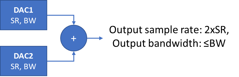
Multiplexing two DACs. SR refers to sample rate, BW refers to bandwidth. Source: Keysight.
“There are two 128GSps 8-bit silicon germanium DACs that are time-interleaved to get a higher speed signal per dimension,” says Pittalá. If the two DACs are shifted in time and added together, the result is a higher sampling rate overall. However, Pittalá points out that while the sample rate is effectively doubled, the overall bandwidth is defined by the individual DACs (see diagram above).
Pittalá also mentions another technique, based on active clocking, that does increase the bandwidth of the system. The multiplexer is clocked and acts like a fast switch between the two DAC channels. “In principle, you can double the bandwidth, ” he says. (See diagram below.)

The Keysight’s M8199B’s improved performance, combined with advances in components such as NTT’s 130GHz indium phosphide amplifier, resulted in over 2Tbps transmission, as detailed in the ECOC 2022 paper. As the baud rate was increased, the modulation scheme used and the net bit rate decreased. (Shown by the red dots on the chart).
In parallel, Keysight worked with Nokia, which used a thin-film lithium niobate modulator for their set-up, a different modulator to NTT’s. The test equipment directly drove the thin-film modulator; no external modulator driver was needed. The system was operated as high as 260GBd, achieving a net bit rate of 800Gbps.
Pittalà notes that while the NTT system differs from Nokia’s, Nokia’s two red points on the extreme right of the chart continue the trajectory of NTT’s six red points as the baud rate increases.
OFC’23 O-band record
The post-deadline papers at the OFC 2023 conference earlier this year did not improve the transmission performances of the ECOC papers.
A post-deadline paper published at OFC 2023 showed a record of coherent transmission in the O-Band. Working with Keysight, McGill University showed 1.6Tbps coherent transmission over 10km using a thin-film lithium niobate modulator. The system operated at 167GBd, used a 64-QAM modulation scheme, and used the Keysight M8199B.
Pittalà expects that at ECOC 2023, to be held in Glasgow in October, new record-breaking transmissions will be announced.
His chart will need updating.
Further information
Thin-film lithium niobate modulators, click here

Ciena advances coherent technology on multiple fronts
- Ciena has unveiled the industry’s first coherent digital signal processor (DSP) to support 1.6-terabit wavelengths
- Ciena announced two WaveLogic 6 coherent DSPs: Extreme and Nano
- WaveLogic 6 Extreme operates at a symbol rate of up to 200 gigabaud (GBd) while the Nano, aimed at coherent pluggables, has a baud rate from 118-140GBd
Part 1: WaveLogic 6 coherent DSPs
Ciena has leapfrogged the competition by announcing the industry’s first coherent DSP operating at up to 200GBd.
The WaveLogic 6 chips are the first announced coherent DSPs implemented using a 3nm CMOS process.
Ciena’s competitors are – or will soon be – shipping 5nm CMOS coherent DSPs. In contrast, Ciena has chosen to skip 5nm and will ship WaveLogic 6 Extreme coherent modems in the first half of 2024.
Using a leading CMOS process enables the cramming of more digital logic and features in silicon. The DSP also operates a faster analogue front-end, i.e. analogue-to-digital converters (ADC) and digital-to-analogue (DAC) converters.
The WaveLogic 6 matches Ciena’s existing WaveLogic 5 family in having two DSPs: Extreme, for the most demanding optical transmission applications, and Nano for pluggable modules.
WaveLogic 6 Extreme is the first announced DSP that supports a 1.6-terabit wavelength; Acacia’s (Cisco) coherent DSP supports 1.2-terabit wavelengths and other 1.2-terabit wavelength DSPs are emerging.
WaveLogic 6 Nano addresses metro-regional networks and data centre interconnect (up to 120km). Here, cost, size, and power consumption are critical. Ciena will offer the WaveLogic 6 in QSFP-DD and OSFP pluggable form factors.
Class 3.5
Network traffic continues to grow exponentially. Ciena notes that the total capacity of its systems shipped between 2010 and 2021 has grown 150x, measured in petabits per second.
Increasing the symbol rate is the coherent engineers’ preferred approach to reduce the cost per bit of optical transport.
Doubling the baud rate doubles the data sent using the same modulation scheme. Alternatively, the data payload can be sent over longer spans.
However, upping the symbol rates increases the optical wavelength’s channel width. Advanced signal processing is needed to achieve further spectral efficiency gains.
One classification scheme of coherent modem symbol rate defines first-generation coherent systems operating at 30-34GBd as Class 1. Class 2 modems double the rate to 60-68GBd. The OIF’s 400ZR standard operating at 64GBd is a Class 2 coherent modem.
Currently-deployed optical transport systems operating at 90-107GBd reside between Class 2 and Class 3 (120-136GBd). Ciena’s WaveLogic 5 Extreme is one example, with its symbol rate ranging from 95-107GBd. Ciena has shipped over 60,000 WaveLogic 5 Extreme DSPs to over 200 customers.
Acacia’s latest CIM-8 coherent modem, now shipping, operates at 140GBd, making it a Class 3 design. Infinera, NEL, and Nokia announced their Class 3 devices before the OFC 2023 conference and exhibition.
Now Ciena, with its 200GBd WaveLogic 6 Extreme, sits alone between Class 3 and Class 4 (240-272GBd).
WaveLogic 6 Extreme
Ciena has extended the performance of all the components of the Extreme-based coherent modem to work at 200GBd.
These components include the DSP’s analogue front-end: the ADCs and DACs, the coherent optics and the modulator drivers and TIAs. All must operate with a 100GHz bandwidth.
To operate at 200GBd, the ADCs and DACs must sample over 200 giga-samples a second. This is pushing ADC and DAC design to the limit.
The coherent modem’s optics and associated electronics must also have a 100GHz operating bandwidth. Ciena developed the optics in-house and is also working with partners to bring the coherent optics to market with a 100GHz bandwidth.
Ciena uses silicon photonics for the Extreme’s integrated coherent receiver (ICR) optics. For the coherent driver modulator (CDM) transmitter, Ciena is using indium phosphide and is also evaluating other technology such as thin-film lithium niobate.
“There are multiple options that are available and being looked at,” says Helen Xenos, senior director of portfolio marketing at Ciena.
Much innovation has been required to achieve the fidelity with 100GHz electro-optics and get the signalling right between the transmitter-receiver and the ASIC, says Xenos.
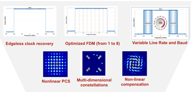
Ciena introduced frequency division multiplexing (FDM) sub-carriers with the WaveLogic 5 Extreme, a technique to help tackle dispersion. With the introduction of edgeless clock recovery, Ciena has created a near-ideal rectangular spectrum with sharp edges.
“First, inside this signal, there are FDM sub-carriers, but you don’t see them because they are right next to each other,” says Xenos. “Getting rid of this dead space between carriers enables more throughput.”
Making the signal’s edges sharper means that wavelengths are packed more tightly, better using precious fibre spectrum. Edgeless clock recovery alone improves spectral efficiency by between 10-13 per cent, says Xenos.
Moving to 3nm allows additional signal processing. As an example, Ciena’s WaveLogic 6 Extreme DSP can select between 1, 2, 4 and 8 sub-carriers based on the dispersion on the link. WaveLogic 5 Extreme supports 4 sub-carrier FDM only.
The baud rate is also adjustable from 67-200GBd, while for the line rate, the WaveLogic 6 supports 200-gigabit to 1.6-terabit wavelengths using probabilistic constellation shaping (PCS).
Another signal processing technique used is multi-dimensional constellation shaping. These are specific modulations that are added to support legacy submarine links.
“For compensated submarine cables that have specific characteristics, they need a specialised type of design also in the DSP,” says Xenos.
Ciena also uses nonlinear compensation techniques to squeeze further performance and allow higher power signals, improving overall link performance.
Ciena can address terrestrial and new and legacy submarine links with the WaveLogic 6 Extreme running these techniques.
Xenos cites performance examples using the enhanced DSP performance of the WaveLogic 6 Extreme.
Using WaveLogic 5, an 800-gigabit wavelength can be sent at 95GBd using a 112.5GHz-wide channel. The 800-gigabit signal can cross several reconfigurable optical add-drop multiplexer (ROADM) hops.
Sending a 1.6-terabit wavelength at 185GBd over a similar link, the signal occupies a 200GHz channel. “And you get better performance because of the extra DSP enhancements,” says Xenos.
The operator Southern Cross has simulated using the WaveLogic 6 Extreme on its network and says the DSP will be able to send one terabit of data over 12,000km.
Optical transport systems benefits
Systems benefits of the Extreme DSP include doubling capacity, transmitting a 1.6-gigabit wavelength, and halving the power consumed per bit.
The WaveLogic 6 Extreme will fit within existing Ciena optical transport kit.
Xenos said the design goal is to get to the next level of cost and power reduction and maximise the network coverage for 800-gigabit wavelengths. This is why Ciena chose to jump to 3nm CMOS for the WaveLogic 6 Extreme, skipping 5nm CMOS.
WaveLogic 6 Nano
The 3nm CMOS WaveLogic 6 Nano addresses pluggable applications for metro and data centre interconnect.
“The opportunity is still largely in front of us [for coherent pluggables],” says Xenos.
The current WaveLogic 5 Nano operating between 31.5-70GBd addresses 100-gigabit to 400-gigabit coherent pluggable applications. These include fixed grid networks using 50GHz channels and interoperable modes such as OpenROADM, 400ZR and 400ZR+. Also supported is the 200-gigabit CableLabs specification.
The WaveLogic 5 Nano is also used in the QSFP-DD module with embedded amplification for high-performance applications.
There is also a new generation of specifications being worked on by standards bodies on client side and line side 800-gigabit and 1.6-terabit interfaces.
Developments mentioned by Xenos include an interoperable probabilistic constellation shaping proposal to be implemented using coherent pluggables.
The advent of 12.8-terabit and 25.6-terabit Ethernet switches gave rise to 400ZR. Now with the start of 51.2-terabit and soon 102.4-terabit switches, the OIF’s 800ZR standard will be needed.

There is also a ‘Beyond 400 Gig’ ITU-T and OpenROADM initiative to combine the interoperable OpenZR+ and the 400-gigabit coherent work of the OpenROADM MSA for a packet-optimised 800-gigabit specification for metro applications.
Another mode is designed to support not just Ethernet but OTN clients.
Lastly, there will also be long-distance modes needed at 400, 600, and 800-gigabit rates.
“With WaveLogic 6 Nano, the intent is to double the capacity within the same footprint,” says Xenos.
In addition to these initiatives, the WaveLogic 6 Nano will address a new application class for much shorter spans – 10km and 20km – at the network edge. The aim is to connect equipment across buildings in a data centre campus, for example.
Some customers want a single channel design and straightforward forward-error correction. Other customers with access to limited capacity will want a wavelength division multiplexed (WDM) solution.
The Nano’s processing and associated optics will be tuned to each application class. “The engineering is done so that we only use the performance and power required for a specific application,” says Xenos.
A Nano-based coherent pluggable connecting campus buildings will differ significantly from a pluggable sending 800 gigabits over 1,000km or across a metro network with multiple ROADM stages, she says.
The WaveLogic 6 Nano will be used with silicon photonics-based coherent optics, but other materials for the coherent driver modulator transmitter may be used.
Availability
Ciena taped out the first 3nm CMOS Extreme and Nano ICs last year.
The WaveLogic 6 Extreme-based coherent modem will be available for trials later this year. Product shipments and network deployments will begin in the first half of 2024.
Meanwhile, shipments of WaveLogic 6 Nano will follow in the second half of 2024.
How to shepherd a company’s technologies for growth

CTO interviews part 3: Dr Julie Eng
- Eng is four months into her new role as CTO of Coherent.
- Previously, she headed Finisar’s transceiver business and then the 3D sensing business, first at Finisar and then at II-VI. II-VI changed its name to Coherent in September 2022
- “CTO is one of these roles that has no universal definition,” says Eng
ulie Eng loved her previous role.
She had been heading II-VI’s (now Coherent’s) 3D sensing unit after being VP of engineering at Finisar’s transceiver business. II-VI bought Finisar in 2019.
She moved across to a new 3D sensing business while still at Finisar. The 3D sensing unit was like a start-up within a large company, she says.
II-VI and Finisar had been competitors in the 3D sensing market. Eng headed the combined units after Finisar’s acquisition.
She enjoyed the role and wasn’t looking to change when the CEO asked her to become Coherent’s CTO.
“To become CTO of the new Coherent – to help define the future of this company which is a five-plus going on six billion dollar company – that is pretty exciting,” says Eng.
The “New” Coherent
Coherent combines a broad portfolio of technologies from II-VI, Finisar, and the firm Coherent which II-VI acquired in 2022.
Just within lasers, Coherent’s portfolio spans from devices 1mm wide that are sold into mobile phones to the former Coherent’s lasers that are meters wide and used for OLED manufacturing.
Being CTO is different from Eng’s line-management roles, which had set, tangible annual goals.
Her role now is to shepherd the company’s technologies and grow the business over the long term.
Eng has been familiarising herself with the company’s technologies. To this aim, Eng is drawing on deep technological expertise across the company’s units.
Luckily, lasers are already covered, she quips.
“One of the things that I always somehow had a knack for is interacting with customers, sensing opportunities, and then figuring out how our technologies can help customers solve their problems,” says Eng.
It is a skill she successfully transferred to the consumer – 3D sensing – business but now it will be needed on a broader scale.
Eng is also making connections across technology units within the company as she seeks to identify new technologies and new market opportunities.
Her CTO role also allows her to engage with every Coherent customer across the company’s many markets.
She admits being CTO is challenging. One issue is grappling with the breadth of technologies the company has. Another is how to assess her works’ impact.
She and the CEO have discussed how best to use her time to benefit the company. Eng has also talked to other companies’ CTOs about the role and what works for them.
“It’s very interesting; CTO is one of these roles that has no universal definition,” says Eng.
Technologies to watch
Eng highlights several developments when asked about noteworthy technologies.
For communications, this is the year when 200 gigabits per lane will likely be achieved.
“The first transceivers I worked on were [SONET/SDH] OC-3 which is 155 megabits per second (Mbps),” she says. “Is wasn’t even a transceiver back then; it was discrete transmitters and receivers.”
That the industry has accelerated technology to achieve multiple lanes of 200 gigabit-per-second (Gbps) in a pluggable module is remarkable, she says.
Eng also notes Coherent’s work on a continuous-wave laser integrated with a Mach-Zehnder modulator – a DMZ – to enable 200 gigabits per lane.
The company is also active in life sciences and health monitoring. Communications, especially during the pandemic, showed its importance in people’s lives. “But life sciences and health-related products have a much more direct impact on people,” says Eng. “That is not something I’ve had direct exposure to.”
Life sciences and health monitoring is a segment where optics and optical devices will play a growing role over time.
Medical devices often originate in research environments such as hospital labs before becoming medical instruments. From the lab, they go to clinical. “What we are talking about here is going from lab to clinical to therapeutics,” she says.
The US Chips Act also heartens Eng: “It was about time for the US to prioritise semiconductors.”
Low-power coherent DSPs
Coherent and ADVA jointly developed a low-power coherent digital signal processor (DSP) and optics design for a 100-gigabit ZR (100ZR) design that fits within a QSFP28 module.
“We have an internal DSP team, and they are developing DSPs for the coherent optics market,” says Eng, adding that having the design team gives Coherent options.
Meanwhile, the debate about direct detection technology versus coherent optics continues.
As optical lane speed increases from 100 gigabits to 200 gigabits, the question remains what reach will direct detection achieve before running out of steam?
With 200 gigabits per lane, 800 gigabit modules can be achieved using four optical lanes, while for 1.6 terabits, eight lanes will be used.
Eng is confident that direct detection will support 10km at these speeds. Beyond 10km, direct detection becomes much more of a challenge, and coherent is an option.
“The real question is will coherent optics meet the size, cost and power consumption expectations of the data centre customers on a timeframe that meets their needs,” says Eng.
Having in-house DSP technology means Coherent can undertake design trade-offs and make the right decisions, she says.
After 1.6 terabits, the design options include increasing the lane rate, using more than eight channels or adopting more advanced modulation schemes.
“We look at the application, the timeline that the product needs to be released, the readiness of the technology, we do measurements – simulations – and we make objective decisions based on the results,” says Eng.
Whatever the prevalent technology is, says Eng, that technology will continue to improve since that is the livelihood of many companies.
“All of us, as an industry, are going to put our all into extending the technologies we currently have,” says Eng. So, when it comes to direct detection versus coherent, everyone will push direct detect technology as far as possible.
“Getting up to 1.6 terabits [using direct detect], that is pretty good,” says Eng. “That is going to last us a pretty long time.”
Materials
Coherent’s toolbox of material systems covers indium phosphide, silicon photonics, and gallium arsenide. It also has silicon carbide, a semiconductor suited for high-power transistors used for power electronics applications.
“We have all the technologies, we use the best technology for the product, and we use good engineering judgement,” says Eng.
Rather than favour indium phosphide or silicon photonics, Eng’s segmentation starts with whether the design is directly modulated or externally modulated.
Until now, up to 50 gigabits per lane has been well served by directly modulated lasers. This has used indium phosphide or, in the case of VCSELs, gallium arsenide.
“In general, directly modulated is the lower cost because the die is tiny, and often it is the lowest power,” says Eng.
But increasing the speed beyond 50Gbps gets more complicated with directly modulated lasers. This is where externally modulated lasers come in.
“Once you are already talking about an externally modulated solution, we start looking at the trade-offs between indium phosphide and silicon photonics,” says Eng.
The laser remains indium phosphide, so the bake-off concerns the modulator and the passive optics.
What indium phosphide brings is better electro-optics performance, while silicon photonics brings the benefits of integration.
“So if there is a high-lane count – lots of passives – or an opportunity to use one laser over multiple modulators, these can be complicated designs, and silicon photonics can help reduce the size,” says Eng.

Pluggables and co-packaged optics
With 200 gigabits per lane becoming available, there is a clear roadmap for 800-gigabits and 1.6-terabit pluggables.
“Customers like pluggables, and I don’t think people should underestimate that,” says Eng, adding that continued innovation will extend their lifetime.
“There are flyover cables between the switch ASIC and the modules, vertical line cards have been proposed, and we have shown board-mounted optical assemblies,” she says.
At some point, co-packaged optics may be the right solution, says Eng. But that will depend on the application’s specification, issues such as bandwidth, size, cost, power consumption and reliability.
“People will only transition to optical input-output when extending pluggables doesn’t make sense anymore,” says Eng. “I think it is probably five-plus years away, but there are probably error bars on that.”
Coherent’s activities include using indium phosphide manufacturing for external laser sources for co-package optics. “And we are working on silicon photonics,” she says.
Coherent is also working on co-packaging VCSELs with high-performance chips. “Not all applications require a 2km reach,” she says.

The coming decade’s opportunities
Eng’s thoughts about the growth opportunities for the coming decade are, not surprisingly, viewed through Coherent’s markets focus.
She highlights four segments: communications, industrial, instrumentation, and electronics.
Fibre-optics communications will continue to grow with bandwidth. The opportunities for innovation include datacom and coherent optics.
She also notes growing interest in free-space optics and satellite communications.
“I see money being spent on that and maybe that is a place where someone like ourselves, with a lot of optics as well as bigger lasers, can play a role,” says Eng.
Precision manufacturing uses lasers in the industrial segment. Eng cites cutting, welding and marking as examples.
“We have elements used for battery manufacturing which is increasing due to electric cars,” she says.
Excimer lasers are also used for OLED and microLED display manufacturing.
“We even have optics in extreme UV steppers [used for advanced process node chip manufacturing],” she says.
For instrumentation, much of the growth is around health life sciences. Coherent makes optics that are used inside PCR testers for COVID-19. It also has engineers working on solid state lasers used for flow cytometry (the sorting of cells). She also cites gene sequencing equipment and medical imaging.
Coherent’s electronics segment refers to the consumer market. Growth here for optics and lasers include AR/VR goggles and the metaverse, wearable health monitoring, and automotive.
For automotive, lasers are used for lidar and in-cabin sensing, such as driver and passenger monitoring.
Silicon carbide is also a growth market, and its uses include the wireless market and power devices for electric vehicles.
“I like the communications market, which we see as growing, but for us, with such a broad portfolio, there are many of these other markets and products that I see as exciting for the remainder of this decade,” says Eng.

Lumentum’s CTO discusses photonic trends
CTO interviews part 2: Brandon Collings
- The importance of moving to parallel channels will only increase given the continual growth in bandwidth.
- Lumentum’s integration of NeoPhotonics’ engineers and products has been completed.
- The use of coherent techniques continues to grow, which is why Lumentum acquired the telecom transmission product lines and staff of IPG Photonics.
“It has changed quite significantly given what Lumentum is engaging in,” he says. “My role spans the entire company; I’m engaged in a lot of areas well beyond communications.”
A decade ago, the main focus was telecom and datacom. Now Lumentum also addresses commercial lasers, 3D sensing, and, increasingly, automotive lidar.
Acquisitions
Lumentum was busy acquiring in 2022. The deal to buy NeoPhotonics closed last August. The month of August was also when Lumentum acquired IPG Photonics’ telecom transmission product lines, including its coherent digital signal processing (DSP) team.
NeoPhotonics’ narrow-linewidth tunable lasers complement Lumentum’s modulators and access tunable modules. Meanwhile, the two companies’ engineering teams and portfolios have now been merged.
NeoPhotonics was active in automotive lidar, but Lumentum stresses it has been tackling the market for several years.
“It’s an area with lots of nuances as to how it is going to be adopted: where, how fast and the cost dependences,” says Collings. “We have been supplying illuminators, VCSELs, narrow-linewidth lasers and other technologies into lidar solutions for several different companies.”
Lumentum gained a series of technological capabilities and some products with the IPG acquisition. “The big part was the DSP capability,” says Collings.
ROADMs
Telecom operators have been assessing IP-over-DWDM anew with the advent of coherent optical modules that plug directly into an IP router.
Cisco’s routed optical networking approach argues the economics of using routers and the IP layer for traffic steering rather than at the optical layer using reconfigurable optical add-drop multiplexers (ROADMs).
Is Lumentum, a leading ROADM technology supplier, seeing such a change?
“I don’t think there is a sea change on the horizon of moving from optical to electrical switching,” says Collings. “The reason is still the same: transceivers are still more expensive than optical switches.”
That balance of when to switch traffic optically or electrically remains at play. Since IP traffic continues to grow, forcing a corresponding increase in signalling speed, savings remain using the optical domain.
“There will, of course, be IP routers in networks but will they take over ROADMs?” says Collings. “It doesn’t seem to be on the horizon because of this growth.”
Meanwhile, the transition to more flexible optical networking using colourless, directionless, contentionless (CDC) ROADMs, is essentially complete.
Lumentum undertook four generations of switch platform design in the last decade to enable CDC-ROADM architectures that are now dominant, says Collings.
Lumentum moved from a simple add-drop to a route-and-select and a colourless, contentionless architecture.
A significant development was Lumentum’s adoption of liquid-crystal-on-silicon (LCOS) technology that enabled twin wavelength-selective switches (WSSes) per node that adds flexibility. LCOS also has enabled a flexible grid which Lumentum knew would be needed.
“We’re increasingly using MEMS technology alongside LCOS to do more complex switching functions embedded in colourless, directionless and contentionless networks today,” says Collings.
Shannon’s limit
If the last decade has been about enabling multiplexing and demultiplexing flexibility, the next challenge will be dealing with Shannon’s limit.
“We can’t stuff much more information into a single optical fibre – or that bit of the amplified spectrum of the optical fibre – and go the same distance,” says Collings. “We’ve sort of tapped out or reached that capacity.”
Adding more capacity requires amplified fibre bandwidth, such as using the L-band alongside the C-band or adding a second fibre.
Enabling such expansion in a cost- and power-efficient way will be fundamental, says Collings, and will define the next generation of optical networks.
Moreover, he expects consumer demand for bandwidth growth to continue. More sensing and more up-hauling of data to the cloud for processing will occur.
Accordingly, optical transceivers will continue to develop over the next decade.
“They are the complement requirement for scaling bandwidth, cost and power effectively,” he says.
Parallelism
Continual growth of bandwidth over the next decade will cause the industry to experience technological ceilings that will drive more parallelism in communications.
“If you look in data centres and datacom interconnects, they have long moved to parallel interface implementations because they felt that bandwidth ceiling from a technological, power dissipation or economic reason.”
Coherent systems have a symbol rate of 128 gigabaud (GBd), and the industry is working on 256GBd systems. Sooner or later, the consensus will be that the symbol rate is fast enough, and it is time to move to a parallel regime.
“In large-scale networks, parallelism is going to be the new thing over the next ten years,” says Collings.
Coherent technology
Collings segments the coherent optical market into three.
There are high-end coherent designs for long-haul transport developed by optical transport vendors such as Ciena, Cisco, Huawei, Infinera and Nokia.
Then there are designs such as 400ZR developed for data centre interconnect. Here a ‘pretty aggressive’ capability is needed but not full-scale performance.
At the lower end, there are application areas where direct-detect optics is reaching its limit. For example, inside the data centre, campus networks and access networks. Here the right solution is coherent or a ‘coherent-light’ technology that is a compromise between direct detection and full-scale coherence used for the long haul.
“So there is emerging this wide continuum of applications that need an equal continuum of coherent technology,” says Collings.
Now that Lumentum has a DSP capability with the IPG acquisition, it can engage with those applications that need solutions that use coherent but may not need the highest-end performance.
800 gigabits and 1.6 terabits
There is also an ongoing debate about the role of coherent for 800-gigabit and 1.6-terabit transceivers, and Collings says the issues remain unclear.
There’s a range of application requirements: 500m, 2km, and 10km. A direct-detect design may meet the 500m application but struggle at 2k and break down at 10km. “There’s a grey area, just in this simple example,” he says.
Also, the introduction of coherent should be nuanced; what is not needed is a long-haul 5,000km DSP. It is more a coherent-light solution or a borrowing from coherent technologies, says Collings: “You’re still trying to solve a problem that you can almost do with direct detect but not quite.”
The aim is to use the minimum needed to accomplish the goal because the design must avoid paying the cost and power to implement the full complement coherent long-haul.
“So that’s the other part of the grey area: how much you borrow?” he says. “And how much do you need to borrow if you’re dealing with 10km versus 2km, or 800 gigabits versus 1.6 terabits.”
Data centres are already using parallel solutions, so there is always the option to double a design through parallelism.
“Eight hundred gigabit could be the baseline with twice as many lanes as whatever we’re doing at 400 gigabits,” he says. “There is always this brute force approach that you need to best if you’re going to bring in new technologies.”
Optical interconnect
Another area Lumentum is active is addressing the issues of artificial intelligence machine-learning clusters. The machine-learning architectures used must scale at an unprecedented rate and use parallelism in processors, multiple such processors per cluster, and multiple clusters.
Scaling processors requires the scaling of their interconnect. This is driving a shift from copper to optics due to the bandwidth growth involved and the distances: 100, 200 and 400 gigabits and lengths of 30-50 meters, respectively.
The transition to an integrated optical interconnect capability will include VCSELs, co-packaged optics, and much denser optical connectivity to connect the graphic processing units (GPUs) rather than architectures based on pluggables that the industry is so familiar with, says Collings.
Co-packaged optics address a power dissipation interconnect challenge and will likely first be used for proprietary interconnect in very high density GPU artificial intelligence clusters.
Meanwhile, pluggable optics will continue to be used with Ethernet switches. The technology is mature and addresses the needs for at least two more generations.
“There’s an expectation that it’s not if but when the switchover happens to co-packaged optics and the Ethernet switch,” says Collings.
Material systems
Lumentum has expertise in several material systems, including indium phosphide, silicon photonics and gallium arsenide.
All these materials have strengths and weaknesses, he says.
Indium phosphide has bandwidth advantages and is best for light generation. Silicon is largely athermal, highly parallelisable and scalable. Staff joining from NeoPhotonics and IPG have strengthened Lumentum’s silicon photonics expertise.
“The question isn’t silicon photonics or indium phosphide. It’s how you get the best out of both material systems, sometimes in the same device,” says Collings. “Sticking in one sandbox is not going to be as competitive as being agile and having the ability to bring those sandboxes together.”