Taking a unique angle to platform design

- A novel design based on a vertical line card shortens the trace length between an ASIC and pluggable modules.
- Reducing the trace length improves signal integrity while maintaining the merits of using pluggables.
- Using the vertical line card design will extend for at least two more generations the use of pluggables with Ethernet switches.
The travelling salesperson problem involves working out the shortest route on a round-trip to multiple cities. It’s a well-known complex optimisation problem.
Novel design that shortens the distance between an Ethernet switch chip and the front-panel optics
Systems engineers face their own complex optimisation problem just sending an electrical signal between two points, connecting an Ethernet switch chip to a pluggable optical module, for example.
Sending the high-speed signal over the link with sufficient fidelity for its recovery requires considerable electronic engineering design skills. And with each generation of electrical signalling, link distances are getting shorter.
In a paper presented at the recent ECOC show, held in Basel, consultant Chris Cole, working with Yamaichi Electronics, outlined a novel design that shortens the distance between an Ethernet switch chip and the front-panel optics.
The solution promises headroom for two more generations of high-speed pluggables. “It extends the pluggable paradigm very comfortably through the decade,” says Cole.
Since ECOC, there are plans to standardise the vertical line card technology in one or more multi-source agreements (MSAs), with multiple suppliers participating.
“This will include OSFP pluggable modules as well as QSFP and QSFP-DD modules,” says Cole.
Shortening links
Rather than the platform using stacked horizontal line cards as is common today, Cole and Yamaichi Electronics propose changing the cards’ orientation to the vertical plane.
Vertical line cards also enable the front-panel optical modules to be stacked on top of each other rather than side-by-side. As a result, the pluggables are closer to the switch ASIC; the furthest the high-speed electrical signalling must travel is three inches (7.6cm). The most distant span between the chip and the pluggable with current designs is typically nine inches (22.8cm).
“The reason nine inches is significant is that the loss is high as we reach 200 gigabits-per-second-per-lane and higher,” says Cole.
Current input-output proposals
The industry is pursuing several approaches to tackle such issues as the issues associated with high-speed electrical signalling and also input-output (I/O) bandwidth density.
One is to use twinaxial cabling instead of electrical traces on a printed circuit board (PCB). Such ‘Twinax’ cable has a lower loss, and its use avoids developing costly advanced-material PCBs.
Other approaches involve bringing the optics closer to the Ethernet switch chip, whether near-packaged optics or the optics and chip are co-packaged together. These approaches also promise higher bandwidth densities.
Cole’s talk focussed on a solution that continues using pluggable modules. Pluggable modules are a low-cost, mature technology that is easy to use and change.
However, besides the radio frequency (RF) challenges that arise from long electrical traces, the I/O density of pluggables is limited due to the size of the connector, while placing up to 36 pluggables on the 1 rack unit-high (1RU) front panel obstructs the airflow used for cooling.
Platform design
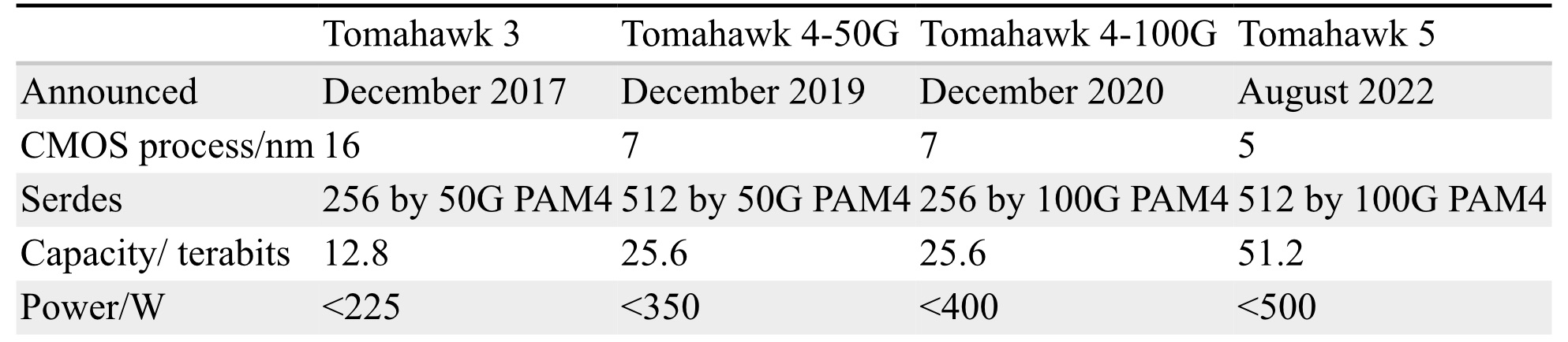
Ethernet switch chips double their capacity every two years. Their power consumption is also rising; Broadcom’s latest Tomahawk 5 consumes 500W.
The power supply a data centre can feed to each platform has an upper limit. It means fewer cards can be added to a platform if the power consumed per card continues to grow.
The average power dissipation per rack is 16kW, and the limit is around 32kW, says Cole. This refers to when air cooling is used, not liquid cooling.
He cites some examples.
A rack of Broadcom’s 12.8-terabit Tomahawk 3 switch chip – either with 32, 1RU or 16, 2RU cards with two chips per card – and associated pluggable optics consume over 30kW.
A 25.6-terabit Tomahawk 4-based chassis supports 16 line cards and consumes 28kW. However, using the recently announced Tomahawk 5, only eight cards can be supported, consuming 27KW.
“The takeaway is that rack densities are limited by power dissipation rather than the line card’s rack unit [measure],” says Cole.
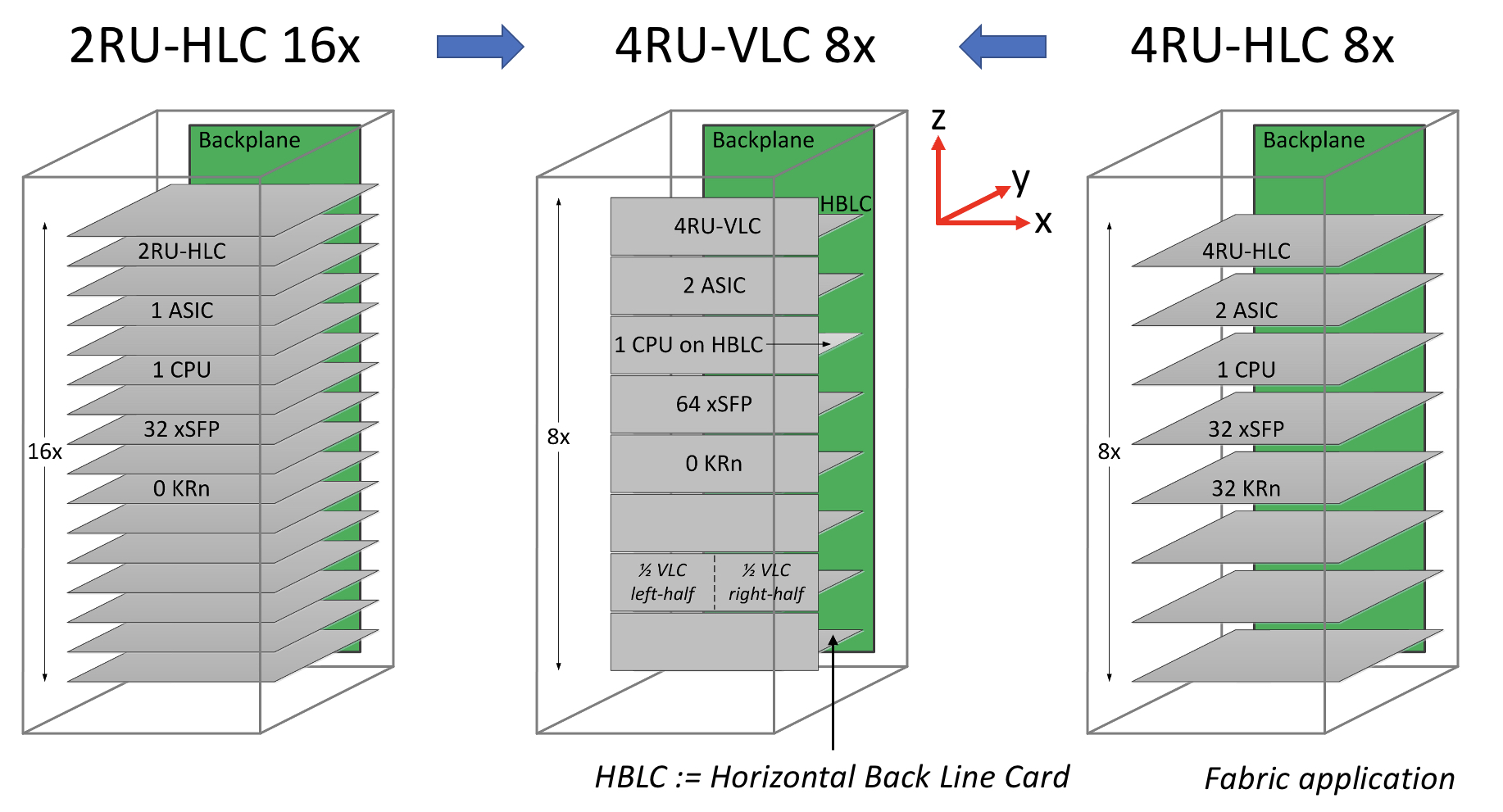
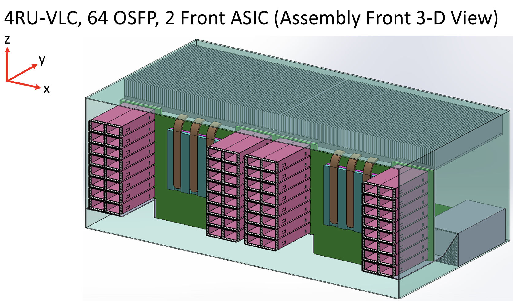
Vertical line card
The vertical line card design is 4RU high. Each card supports two ASICs on one side and 64 cages for the OSFP modules on the other.
A 32RU chassis can thus support eight vertical cards or 16 ASICs, equivalent to the chassis with 16 horizontal 2RU line cards.
The airflow for the ASICs is improved, enabling more moderate air fans to be used compared to 1RU or 2RU horizontal card chassis designs. There is also airflow across the modules.
“The key change in the architecture is the change from a horizontal card to a vertical card while maintaining the pluggable orientation,” says Cole.
As stated, the maximum distance between an ASIC and the pluggables is reduced to three inches, but Cole says the modules can be arranged around the ASIC to minimise the length to 2.5 inches.
Alternatively, if the height of the vertical card is an issue, a 3RU card can be used instead, which results in a maximum trace length of 3.5 inches. “[In this case], we don’t have dedicated air intakes for the CPU,” notes Cole.
Cole also mentioned the option of a 3RU vertical card that houses one ASIC and 64 OSFP modules. This would be suitable for the Tomahawk 5. However, here the maximum trace length is five inches.
Vertical connectors
Yamaichi Electronics has developed the vertical connectors needed to enable the design.
Cole points out that, unlike a horizontal connector, a vertical one uses equal-length contacts. This is not the case for a flat connector, resulting in performance degradation since a set of contacts has to turn and hence has a longer length.
Cole showed the simulated performance of an OSFP vertical connector with an insertion loss of over 70GHz.
“The loss up to 70GHz demonstrates the vertical connector advantage because it is low and flat for all the leads,” says Cole. “So this [design] is 200-gigabit ready.”
He also showed a vertical connector for the OSFP-XD with a similar insertion loss performance.
Also shown was a comparison with results published for Twinax cables. Cole says this indicates that the loss of a three-inch PCB trace is less than the loss of the cable.
“We’ve dramatically reduced the RF maximum length, so we had solved the RF roadblock problem, and we maintain the cost-benefit of horizontal line cards,” says Cole.
The I/O densities may be unchanged, but it preserves the mature technology’s benefits. “And then we get a dramatic improvement in cooling because there are no obstructions to airflow,” says Cole.
Vladimir Kozlov, CEO of the market research firm, LightCounting, wondered in a research note whether the vertical design is a distraction for the industry gearing up for co-packaged optics.
“Possibly, but all approaches for reducing power consumption on next-generation switches deserve to be tested now,” said Kozlov, adding that adopting co-packaged optics for Ethernet switches will take the rest of the decade.
“There is still time to look at the problem from all angles, literally,” said Kozlov

ECOC '22 Reflections - Part 2

Gazettabyte is asking industry and academic figures for their thoughts after attending ECOC 2022, held in Basel, Switzerland. In particular, what developments and trends they noted, what they learned, and what, if anything, surprised them.
In Part 2, Broadcom‘s Rajiv Pancholy, optical communications advisor, Chris Cole, LightCouting’s Vladimir Kozlov, Ciena’s Helen Xenos, and Synopsys’ Twan Korthorst share their thoughts.
Rajiv Pancholy, Director of Hyperscale Strategy and Products Optical Systems Division, Broadcom*
The buzz at the show reminded me of 2017 when we were in Gothenburg pre-pandemic, and that felt nice.
Back then, COBO (Consortium for On-Board Optics) was in full swing, the CWDM8 multi-source agreement (MSA) was just announced, and 400-gigabit optical module developments were the priority.
This year, I was pleased to see the show focused on lower power and see co-packaged optics filter into all things ECOC.
Broadcom has been working on integrating a trans-impedance amplifier (TIA) into our CMOS digital signal processor (DSP), and the 400-gigabit module demonstration on the show floor confirmed the power savings integration can offer.
Integration impacts power and cost but it does not stop there. It’s also about what comes after 2nm [CMOS], what happens when you run out of beach-front area, and what happens when the maximum power in your rack is not enough to get all of its bandwidth out.
It is the idea of fewer things and more efficient things that draws everyone to co-packaged optics.
The OIF booth showcased some of the excitement behind this technology that is no longer a proof-of-concept.
Moving away from networking and quoting some of the ideas presented this year at the AI Hardware Summit by Alexis Bjorlin, our industry needs to understand how we will use AI, how we will develop AI, and how we will enable AI.
These were in the deeper levels of discussions at ECOC, where we as an industry need to continue to innovate, disagree, and collaborate.
Chris Cole, Optical Communications Advisor
I don’t have many substantive comments because my ECOC was filled with presentations and meetings, and I missed most of the technical talks and market focus presentations.
It was great to see a full ECOC conference. This is a good sign for OFC.
Here is an observation of what I didn’t see. There were no great new silicon photonics products, despite continued talk about how great it is and the many impressive research and development results.
Silicon photonics remains a technology of the future. Meanwhile, other material systems continue to dominate in their use in products.
Vladimir Kozlov, CEO of LightCounting
I am surprised by the progress made by thin-film lithium niobate technology. There are five suppliers of these devices now: AFR, Fujitsu, Hyperlight, Liobate, and Ori-chip.
Many vendors also showed transceivers with thin-film lithium niobate modulators inside.
Helen Xenos, senior director of portfolio marketing at Ciena
One key area to watch right now is what technology will win for the next Ethernet rates inside the data centre: intensity-modulation direct detection (IMDD) or coherent.
There is a lot of debate and discussion happening, and several sessions were devoted to this topic during the ECOC Market Focus.
Twan Korthorst, Group Director Photonic Solutions at Synopsys.
My main observations are from the exhibition floor; I didn’t attend the technical conference.
ECOC was well attended, better than previous shows in Dublin and Valencia and, of course, much better than Bordeaux (the first in-person ECOC in the Covid era).
I spent three days talking with partners, customers and potential customers, and I am pleased about that.
I didn’t see the same vibe around co-packaged optics as at OFC; not a lot of new things there.
There is a feeling of what will happen with the semiconductor/ datacom industry. Will we get a downturn? How will it look? In other words, I noticed some concerns.
On the other hand, foundries are excited about the prospects for photonic ICs and continue to invest and set ambitious goals.

Tencent makes its co-packaged optics move

- Tencent is the first hyperscaler to announce it is deploying a co-packaged optics switch chip
- Tencent will use Broadcom’s Humboldt that combines its 25.6-terabit Tomahawk 4 switch chip with four optical engines, each 3.2 terabit-per-second (Tbps)
Part 2: Broadcom’s co-packaged optics
Tencent will use Broadcom’s Tomahawk 4 switch chip co-packaged with optics for its data centres.
“We are now partnered with the hyperscaler to deploy this in a network,” says Manish Mehta, vice president of marketing and operations optical systems division, Broadcom. “This is a huge step for co-packaged optics overall.”
Broadcom demonstrated a working version of a Humboldt switch at OFC earlier this year.
The Chinese hyperscaler will use Broadcom’s 25.6Tbps Tomahawk 4 Humboldt, a hybrid design where half of the chip’s input-output (I/O) is optical and half is the chip’s serialisers-deserialisers (serdes) that connect to pluggable modules on the switch’s front panel.
Four Broadcom 3.2-terabit silicon photonics-based optical engines are co-packaged alongside the Tomahawk 4 chip to implement 12.8Tbps of optical I/O.
Broadcom demonstrated a working version of a Humboldt switch at OFC earlier this year.
Co-packaged optics
Broadcom started its co-packaged optics development work in 2019.
“One of the reasons for our investment in co-packaged optics was that we did see firsthand the ongoing limits of copper interconnect being approached,” says Mehta.
The transmission reach of copper links continues to shrink as the signalling speed has increased from 25 gigabits-per-second (Gbps) non-return to zero (NRZ) to PAM-4 (4-level pulse amplitude modulation) based signalling at 56Gbps, 112Gbps and, in the coming years, 224Gbps. Power consumption is also rising with each speed hike.
Broadcom says data centres now use 1 million optical interconnects, but that much of the connectivity is still copper-based, linking adjacent racks and equipment within the rack.
“Hyperscalers spend ten times more on interconnects than switching silicon,” says Mehta. Given these trends, there needs to be a continual improvement in the power profile, cost and scaled manufacturing of optical interconnect, he says.
In the short term, what is driving interest in co-packaged optics is overcoming the limitations of copper, says Broadcom.
In early 2021, Broadcom detailed at a JP Morgan event its co-packaged optics roadmap. Outlined was the 25.6-terabit Humboldt to be followed by Bailly, a 51.2-terabit all co-packaged optics design using Broadcom’s Tomahawk 5 switch chip which is now sampling.
Humboldt uses DR4 (4×100-gigabit using 4 fibres) whereas the 51.2-terabit Bailly will add multiplexing-demultiplexing and use the FR4 specification (4×100-gigabit wavelengths per fibre).
Technology and partners
Broadcom’s in-house technology includes lasers (VCSELs and EMLs), mixed-signal expertise (trans-impedance amplifiers and drivers), and silicon photonics, as well as its switch chips.
Broadcom uses a remote laser source for its co-packaged optics design. Placing the laser away from the package (the switch chip and optics) means no cooling is needed.
Broadcom is working with 15 partners to enable its co-packaged optics, highlighting the breadth of expertise required and the design complexity.
There are two prominent use cases for the hybrid I/O Humboldt.
One is for top-of-rack switches, where the electrical interfaces support short-reach copper links connecting the servers in a rack, while the optical links connect the top-of-rack box to the next layer of aggregation switching.
The second use is at the aggregation layer, where the electrical I/O connects other switches in the rack while the optical links connect to switch layers above or below the aggregation layer.
“There is a use case for having pluggable ports where you can deploy low-cost direct-attached copper,” says Mehta.
Broadcom says each data centre operator will have their own experience with their manufacturing partners as they deploy co-packaged optics. Tencent has decided to enter the fray with 25.6-terabit switches.
“It is not just Broadcom developing the optical solution; it is also ensuring that our manufacturing partner is ready to scale,” says Mehta.
Ruijie Networks is making the two-rack-unit (2RU) switch platform for Tencent based on Broadcom’s co-packaged optics solution. The co-packaged optics interfaces are routed to 16 MPO connectors while the switch supports 32, 400-gigabit QSFP112 modules.
“It’s always important to have your lead partner [Tencent] for any deployment like this, someone you’re working closely with to get it to market,” says Mehta. “But there is interest from other customers as well.”
Cost and power benefits
Broadcom says co-packaged optics will lower the optical cost-per-bit by 40 per cent while the system (switch platform) power savings will be 30 per cent.
Humboldt more than halves the power compared to using pluggables. Broadcom’s co-packaged optics consumes 7W for each 800-gigabits of bandwidth, whereas an equivalent 800-gigabit optical module consumes 16-18W.
Its second-generation design will embrace 5nm CMOS rather than 7nm and still more than halve the power: an 800-gigabit pluggable will consume 14-15W, whereas it will be 5.5W for the same co-packaged optics bandwidth.
Broadcom will move to CMOS for its second-generation electrical IC; it uses silicon germanium at present.
Power and operational cost savings are a longer-term benefit for data centre operators, says Broadcom. A more immediate concern is the growing challenge of managing the thermal profile when designing switching systems. “The amount of localised heat generation of these components is making systems quite challenging,” says Mehta.
A co-packaged design eliminates pluggables, making system design easier by improving airflow via the front panel and reducing the power required for optical interconnect.
“They’ve been telling us this directly,” says Mehta. “It’s been a pretty good testimonial to the benefits they can see for system design and co-packaged optics.”
Roadmap
At OFC 2022, Broadcom also showed a mock-up of Bailly, a 51.2 terabit switch chip co-packaged with eight 6.4Tbps optical engines.
Broadcom will offer customers a fully co-packaged optics Tomahawk 5 design but has not given a date.
Since Broadcom has consistently delivered a doubling of switch silicon capacity every 24 months, a 102.4-terabit Tomahawk 6 is scheduled to sample in the second half of 2024.
That timescale suggests it will be too early to use 224Gbps serdes being specified by the OIF. Indeed, Mehta believes 112Gbps serdes will have “a very long life”.
That would require the next-generation 102.2Tbps to integrate 1024, 100Gbps serdes on a die. Or, if that proves too technically challenging, then, for the first time, Broadcom’s switching ASIC may no longer be a monolithic die.
Broadcom’s networking group is focused on high-speed serial electrical interfaces. But the company is encouraged by developments such as the open standard UCIe for package interconnect, which looks at slower, wider parallel electrical interfaces to support chiplets. UCIe promises to benefit co-packaged optics.
Broadcom’s view is that it is still early with many of these design challenges.
“Our goal is to understand when we need to be ready and when we need to be launching our silicon on the optical side,” says Mehta. “That’s something we are working towards; it’s still not clear yet.”

Broadcom samples the first 51.2-terabit switch chip

- Broadcom’s Tomahawk 5 marks the era of the 51.2-terabit switch chip
- The 5nm CMOS device consumes less than 500W
- The Tomahawk 5 uses 512, 100-gigabit PAM-4 (4-level pulse amplitude modulation) serdes (serialisers-deserialisers)
- Broadcom will offer a co-packaged version combining the chip with eight 6.4 terabit-per-second (Tbps) optical engines
Part 1: Broadcom’s Tomahawk 5
Broadcom is sampling the world’s first 51.2-terabit switch chip.
With the Tomahawk 5, Broadcom continues to double switch silicon capacity every 24 months; Broadcom launched the first 3.2-terabit Tomahawk was launched in September 2014.
“Broadcom is once again first to market at 51.2Tbps,” says Bob Wheeler, principal analyst at Wheeler’s Network. “It continues to execute, while competitors have struggled to deliver multiple generations in a timely manner.”
Tomahawk family
Hyperscalers use the Tomahawk switch chip family in their data centres.
Broadcom launched the 25.6-terabit Tomahawk 4 in December 2019. The chip uses 512 serdes, but these are 50-gigabit PAM-4. At the time, 50-gigabit PAM-4 matched the optical modules’ 8-channel input-output (I/O).
Certain hyperscalers wanted to wait for 400-gigabit optical modules using four 100-gigabit PAM-4 electrical channels, so, in late 2020, Broadcom launched the Tomahawk4-100G switch chip, which employs 256, 100-gigabit PAM-4 serdes.
Tomahawk 5 doubles the 100-gigabit PAM-4 serdes to 512. However, given that 200-gigabit electrical interfaces are several years off, Broadcom is unlikely to launch a second-generation Tomahawk 5 with 256, 200-gigabit PAM-4 serdes.
Switch ICs
Broadcom has three switch chip families: Trident, Jericho and the Tomahawk.
The three switch chip families are needed since no one switch chip architecture can meet all the markets’ requirements.
With its programable pipeline, Trident targets enterprises, while Jericho targets service providers.
According to Peter Del Vecchio, Broadcom’s product manager for the Tomahawk and Trident lines, there is some crossover. For example, certain hyperscalers favour the Trident’s programmable pipeline for their top-of-rack switches, which interface to the higher-capacity Tomahawk switches chips at the aggregation layer.
Monolithic design
The Tomahawk 5 continues Broadcom’s approach of using a monolithic die design.
“It [the Tomahawk5] is not reticule-limited, and going to [the smaller] 5nm [CMOS process] helps,” says Del Vecchio.
The alternative approach – a die and chiplets – adds overall latency and consumes more power, given the die and chiplets must be interfaced. Power consumption and signal delay also rise whether a high-speed serial or a slower, wider parallel bus is used to interface the two.
Equally, such a disaggregated design requires an interposer on which the two die types sit, adding cost.
Chip features
Broadcom says the capacity of its switch chips has increased 80x in the last 12 years; in 2010, Broadcom launched the 640-gigabit Trident.
Broadcom has also improved energy efficiency by 20x during the same period.
“Delivering less than 1W per 100Gbps is pretty astounding given the diminishing benefits of moving from a 7nm to a 5nm process technology,” says Wheeler.
“In general, we have achieved a 30 per cent plus power savings between Tomahawk generations in terms of Watts-per-gigabit,” says Del Vecchio.

These power savings are not just from advances in CMOS process technology but also architectural improvements, custom physical IP designed for switch silicon and physical design expertise.
“We create six to eight switch chips every year, so we’ve gotten very good at optimising for power,” says Del Vecchio
The latest switch IC also adds features to support artificial intelligence (AI)/ machine learning, an increasingly important hyperscaler workload.
AI/ machine learning traffic flows have a small number of massive ‘elephant’ flows alongside ‘mice’ flows. The switch chip adds elephant flow load balancing to tackle congestion that can arise when the two flow classes mix.
“The problem with AI workloads is that the flows are relatively static so that traditional hash-based load balancing will send them over the same links,” says Wheeler. “Broadcom has added dynamic balancing that accounts for link utilisation to distribute better these elephant flows.”
The Tomahawk 5 also provides more telemetry information so data centre operators can better see and tackle overall traffic congestion.
The chip has added virtualisation support, including improved security of workloads in a massively shared infrastructure.
Del Vecchio says that with emerging 800-gigabit optical modules and 1.6 terabit ones on the horizon, the Tomahawk 5 is designed to handle multiples of 400 Gigabit Ethernet (GbE) and will support 800-gigabit optical modules.
The chip’s 100-gigabit physical layer interfaces are combined to form 800 gigabit (8 by 100 gigabit), which is fed to the MAC, packet processing pipeline and the Memory Management Unit to create a logical 800-gigabit port. “After the MAC, it’s one flow, not at 400 gigabits but now at 800 gigabits,” says Del Vecchio.
Market research firm, Dell’Oro, says that 400GbE accounts for 15 per cent of port revenues and that by 2026 it will rise to 57 per cent.
Broadcom also cites independent lab test data showing that its support for RDMA over Converged Ethernet (RoCE) matches the performance of Infiniband.
“We’re attempting to correct the misconception promoted by competition that Infiniband is needed to provide good performance for AI/ machine learning workloads,” says Del Vecchio. The tests used previous generation silicon, not the Tomahawk 5.
“We’re saying this now since machine learning workloads are becoming increasingly common in hyperscale data centres,” says Del Vecchio.
As for the chip’s serdes, they can drive 4m of direct attached copper cabling, with sufficient reach to connect equipment within a rack or between two adjacent racks.
Software support
Broadcom offers a software development kit (SDK) to create applications. The same SDK is common to all three of its switch chip families.
Broadcom also supports the Switch Abstraction Interface (SAI). This standards-based programming interface sits on top of the SDK, allowing the programming of switches independent of the silicon provider.
Broadcom says some customers prefer to use its custom SDK. It can take time for changes to filter up, and a customer may want something undertaken that Broadcom can develop quickly using its SDK.
System benefits
Doubling the switch chip’s capacity every 24 months delivers system benefits.That is because implementing a 51.2-terabit switch using the current generation Tomahawk 4 requires six such devices.

Now a single 2-rack-unit (2RU) Tomahawk 5 switch chip can support 64 by 800-gigabit, 128 by 400-gigabit and 256 by 200-gigabit modules.
These switch boxes are air-cooled, says Broadcom.
Co-packaged optics
In early 2021 at a J.P Morgan analyst event, Broadcom revealed its co-packaged optics roadmap that highlighted Humboldt, a 25.6-terabit switch chip co-packaged with optics, and Bailly, a 51.2-terabit fully co-packaged optics design.
At OFC 2022, Broadcom demonstrated a 25.6Tbps switch that sent half of the traffic using optical engines.
Also shown was a mock-up of Bailly, a 51.2 terabit switch chip co-packaged with eight optical engines, each at 6.4Tbps.
Broadcom will offer customers a fully co-packaged optics Tomahawk 5 design but has not yet given a date.
Broadcom can also support a customer if they want tailored connectivity with, say, 3/4 of the Tomahawk 5 interfaces using optical engines and the remainder using electrical interfaces to front panel optics.

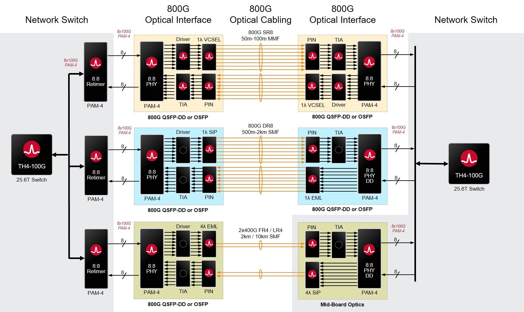
Enabling 800-gigabit optics with physical layer ICs
Broadcom recently announced a family of 800-gigabit physical layer (PHY) chips. The device family is the company’s first 800-gigabit ICs with 100-gigabit input-output (I/O) interfaces.
Source: Broadcom
Moving from 50-gigabit to 100-gigabit-based I/O enables a new generation of 800-gigabit modules aligned with the latest switch chips.
“With the switch chip having 100-gigabit I/Os, PHYs are needed with the same interfaces,” says Machhi Khushrow, senior director of marketing, physical layer products division at Broadcom.
Broadcom’s latest 25.6 terabit-per-second (Tbps) Tomahawk 4 switch chip using 100-gigabit I/O was revealed at the same time.
800-gigabit PHY devices
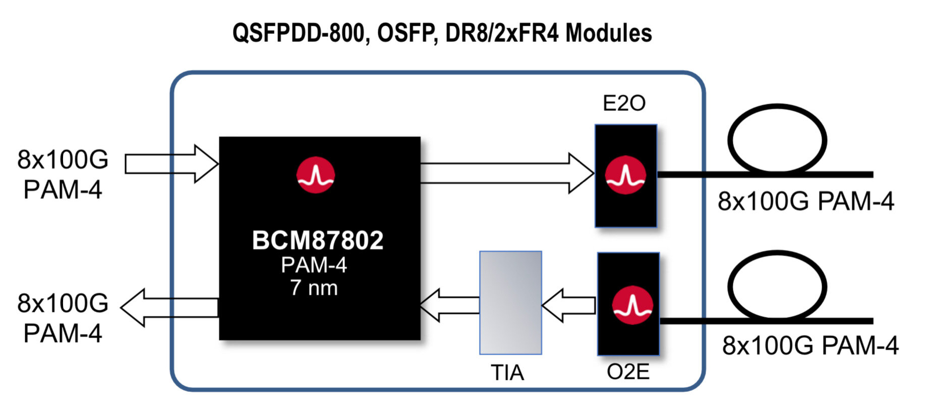
The portfolio comprises three 800-gigabit PHY ICs. All operate at a symbol rate of 53 gigabaud, use 4-level pulse amplitude modulation (PAM-4) and are implemented in a 7nm CMOS process.
Two devices are optical PHYs: the BCM87800 and the BCM87802. These ICs are used within 800-gigabit optical modules such as the QSFP-DD800 and the OSFP form factors. The difference between the two chips is that the BCM87802 includes an integrated driver.
The third PHY - the BCM87360 - is a retimer IC used on line cards. Whether the chip is needed depends on the line card design and signal-integrity requirements; for example, whether the line card is used within a pizza box or part of a chassis-based platform.
Source: Broadcom
“If it is a higher-density card that is relatively small, it may only need 15 per cent of the ports with retimers,” says Khushrow. “If the line card is larger, where things fan out to longer traces, retimers may be needed for all the ports.”
All three 800-gigabit PHYs have eight 100-gigabit transmit and eight receive channels (8:8, as shown in the top diagram).
Applications
The optical devices support several 800-gigabit module designs that use either silicon photonics, directly modulated lasers (DMLs) or externally-modulated lasers (EMLs).
The 800-gigabit PHYs support the DR8 module (8 single-mode fibres, 500m reach), two 400-gigabit DR4 (4 single-mode fibres, 500m) or two FR4 in a module (each 4 wavelengths on a single-mode fibre, 2km) as well as the SR8, a parallel VCSEL-based design with a reach of 100m over parallel multi-mode fibre.
Timescales
Given the availability of these PHYs and that 800-gigabit modules will soon appear, will the development diminish the 400-gigabit market opportinity?
“This is independent of 400-gigabit [module] deployments,” says Khushrow.
The hyperscalers are deploying different architectures. There are hyperscalers that are only now transitioning to 200-gigabit modules while others are transitioning to 400- gigabit. They will all transition to 800 gigabit, he says: “How and when they transition are all at different points.”
Some of the hyperscalers deploying 400-gigabit modules are looking at 800 gigabit, and their deployment plans are maybe two to three years out. “We don’t expect 800 gigabit to cannibalise 400 gigabit, at least not in the near term,” he says.
Broadcom says 800-gigabit modules to ship in the second half of this year. “It all depends on how the switch infrastructure, line cards and optics become available,” says Khushrow.
Next developments
The landscape for high-speed networking in the data centre is changing and optics is moving closer to the switch chip, whether it is on-board optics or co-packaged optics.
“People are looking at both options,” says Khushrow.”It depends on the architecture of the data centre whether they use on-board optics or co-packaged optics.”
Meanwhile, the OIF is working on a 200-gigabit electrical interface standard.
Co-packaged optics is challenging and the technology has its own issues whereas optical transceivers are easier to use and deploy, says Khushrow.
Current industry thinking is that some form of co-packaged optics will be used with the adevnt of next-generation 51.2-terabit switch chips. But even with such capacity switches, pluggables will continue to be used, he says.
There will still be a need for PHYs, whether for pluggables, co-packaged designs or on the linecard.
“We will continue to provide those on our roadmap,” says Khushrow. “It is just a matter of what the form factor will be, whether it will be a packaged part or a die part.”

Switch chips not optics set the pace in the data centre
Broadcom is doubling the capacity of its switch silicon every 18-24 months, a considerable achievement given that Moore’s law has slowed down.
Last December, Broadcom announced it was sampling its Tomahawk 3 - the industry’s first 12.8-terabit switch chip - just 14 months after it announced its 6.4-terabit Tomahawk 2.
 Rochan SankarSuch product cycle times are proving beyond the optical module makers; if producing next-generation switch silicon is taking up to two years, optics is taking three, says Broadcom.
“Right now, the problem with optics is that they are the laggards,” says Rochan Sankar, senior director of product marketing at switch IC maker, Broadcom. “The switching side is waiting for the optics to be deployable.”
The consequence, says Broadcom, is that in the three years spanning a particular optical module generation, customers have deployed two generations of switches. For example, the 3.2-terabit Tomahawk based switches and the higher-capacity Tomahawk 2 ones both use QSFP28 and SFP28 modules.
In future, a closer alignment in the development cycles of the chip and the optics will be required, argues Broadcom.
Switch chips
Broadcom has three switch chip families, each addressing a particular market. As well as the Tomahawk, Broadcom has the Trident and Jericho families (see table).

All three chips are implemented using a 16nm CMOS process. Source: Broadcom/ Gazettabyte.
“You have enough variance in the requirements such that one architecture spanning them all is non-ideal,” says Sankar.
The Tomahawk is a streamlined architecture for use in large-scale data centres. The device is designed to maximise the switching capacity both in terms of bandwidth-per-dollar and bandwidth-per-Watt.
“The hyperscalers are looking for a minimalist feature set,” says Sankar. They consider the switching network as an underlay, a Layer 3 IP fabric, and they want the functionality required for a highly reliable interconnect for the compute and storage, and nothing more, he says.
Right now, the problem with optics is that they are the laggards
Production of the Tomahawk 3 integrated circuit (IC) is ramping and the device has already been delivered to several webscale players and switch makers, says Broadcom.
The second, Trident family addresses the enterprise and data centres. The chip includes features deliberately stripped from the Tomahawk 3 such as support for Layer 2 tunnelling and advanced policy to enforce enterprise network security. The Trident also has a programmable packet-processing pipeline deemed unnecessary inlarge-scale data centres.
But such features are at the expense of switching capacity. “The Trident tends to be one generation behind the Tomahawk in terms of capacity,” says Sankar. The latest Trident 3 is a 3.2-terabit device.
The third, Jericho family is for the carrier market. The chip includes a packet processor and traffic manager and comes with the accompanying switch fabric IC dubbed Ramon. The two devices can be scaled to create huge capacity IP router systems exceeding 200 terabits of capacity. “The chipset is used in many different parts of the service provider’s backbone and access networks,” says Sankar. The Jericho 2, announced earlier this year, has 10 terabits of capacity.
Trends
Broadcom highlights several trends driving the growing networking needs within the data centre.
One is how microprocessors used within servers continue to incorporate more CPU cores while flash storage is becoming disaggregated. “Now the storage is sitting some distance from the compute resource that needs very low access times,” says Sankar.
The growing popularity of public cloud is also forcing data centre operators to seek greater servers utilisation to ‘pack more tenants per rack’.
There are also applications such as deep learning that use other computing ICs such as graphics processor units (GPUs) and FPGAs. “These push very high bandwidths through the network and the application creates topologies where any element can talk to any element,” says Sankar. This requires a ‘flat’ networking architecture that uses the fewest networking hops to connect the communicating nodes.
Such developments are reflected in the growth in server links to the first level or top-of-rack (TOR) switches, links that have gone from 10 to 25 to 50 and 100 gigabits. “Now you have the first 200-gigabit network interface cards coming out this year,” says Sankar.
Broadcom has been able to deliver 12.8 terabits-per-second in 16nm, whereas some competitors are waiting for 7nm
Broadcom says the TOR switch is not the part of the data centre network experiencing greatest growth. Rather, it is the layers above - the leaf-and-spine switching layers - where bandwidth requirements are accelerating the most. This is because the radix - the switch’s inputs and outputs - is increasing with the use of equal-cost multi-path (ECMP) routing. ECMP is a forwarding technique to distribute the traffic over multiple paths of equal cost to a destination port. “The width of the ECMP can be 4-way, 8-way and 16-way,” says Sankar. “That determines the connectivity to the next layer up.”
It is such multi-layered leaf-spine architectures that the Tomahawk 3 switch silicon addresses.
Tomahawk 3
The Tomahawk 3 is implemented using a 16nm CMOS process and features 256 50-gigabit PAM-4 serialiser-deserialiser (serdes) interfaces to enable the 12.8-terabit throughput.
“Broadcom has been able to deliver 12.8 terabits-per-second in 16nm, whereas some competitors are waiting for 7nm,” says Bob Wheeler, vice president and principal analyst for networking at the Linley Group.
Sankar says Broadcom undertook significant engineering work to move from the 16nm Tomahawk 2’s 25-gigabit non-return-to-zero serdes to a 16nm-based 50G PAM-4 design. The resulting faster serdes design requires only marginally more die area while reducing the gigabit-per-Watt measure by 40 percent.
The Tomahawk 3 also features a streamlined packet-processing pipeline and improved shared buffering. In the past, a switch chip could implement one packet-processing pipeline, says Wheeler. But at 12.8 terabit-per-second (Tbps), the aggregate packet rate exceeds the capacity of a single pipeline. “Broadcom implements multiple ingress and egress pipelines, each connected with multiple port blocks,” says Wheeler. The port blocks include MACs and serdes. “The hard part is connecting the pipelines to a shared buffer, and Broadcom doesn’t disclose details here.”
 Source: Broadcom.
The chip also has telemetry support that exposes packet information to allow the data centre operators to see how their networks are performing.
Adopting a new generation of switch silicon also has system benefits.
One is reducing the number of hops between endpoints to achieve a lower latency. Broadcom cites how a 128x100 Gigabit Ethernet (GbE) platform based on a single Tomahawk 3 can replace six 64x100GbE switches in a two-tier arangement. This reduces latency by 60 percent, from 1 microsecond to 400 nanoseconds.
There are also system cost and power consumption benefits. Broadcom uses the example of Facebook’s Backpack modular switch platform. The 8 rack unit (RU) chassis uses two tiers of switches - 12 Tomahawk chips in total. Using the Tomahawk 3, the chassis can be replaced with a 1RU platform, reducing the power consumption by 75 percent and system cost by 85 percent.
Many in the industry have discussed the possibility of using the next 25.6-terabit generation of switch chip in early trials of in-package optics
Aligning timelines
Both the switch-chip vendors and the optical module players are challenged to keep up with the growing networking capacity demands of the data centre. The fact that next-generation optics takes about a year longer than the silicon is not new. It happened with the transition from 40-gigabit QSFP+ to 100-gigabit QSFP28 optical modules and now from the 100-gigabit QSFP28 to 200 gigabit QSFP56 and 400-gigabit QSFP-DD production.
“400-gigabit optical products are currently sampling in the industry in both OSFP and QSFP-DD form factors, but neither has achieved volume production,” says Sankar.
Broadcom is using 400-gigabit modules with its Tomahawk 3 in the lab, and customers are doing the same. However, the hyperscalers are not deploying Tomahawk-3 based data center network designs using 400-gigabit optics. Rather, the switches are using existing QSFP28 interfaces, or in some cases 200-gigabits optics. But 400-gigabit optics will follow.
The consequence of the disparity in the silicon and optics development cycles is that while the data centre players want to exploit the full capacity of the switch once it becomes available, they can’t. This means the data centre upgrades conducted - what Sankar calls ‘mid-life kickers’ - are costlier to implement. In addition, given that most cloud data centres are fibre-constrained, doubling the number of fibres to accommodate the silicon upgrade is physically prohibitive, says Broadcom.
“The operator can't upgrade the network any faster than the optics cadence, leading to a much higher overall total cost of ownership,” says Sankar. They must scale out to compensate for the inability to scale up the optics and the silicon simultaneously.
Optical I/O
Scaling the switch chip - its input-output (I/O) - presents its own system challenges. “The switch-port density is becoming limited by the physical fanout a single chip can support, says Sankar: “You can't keep doubling pins.”
It will be increasingly challenging to increase the input-output (I/O) to 512 or 1024 serdes in future switchchips while satisfying the system link budget, and achieving both in a power-efficient manner. Another reason why aligning the scaling of the optics and the serdes speeds with the switching element is desirable, says Broadcom.
Broadcom says electrical interfaces will certainly scale for its next-generation 25.6-terabit switch chip.
Linley Group’s Wheeler expects the 25.6-terabit switch will be achieved using 256 100-gigabit PAM4 serdes. “That serdes rate will enable 800 Gigabit Ethernet optical modules,” he says. “The OIF is standardising serdes via CEI-112G while the IEEE 802.3 has the 100/200/400G Electrical Interfaces Task Force running in parallel.”
But system designers already acknowledge that new ways to combine the switch silicon and optics are needed.
“One level of optimisation is the serdes interconnect between the switch chip and the optical module itself,” says Sankar, referring to bringing of optics on-board to shorten the electrical paths the serdes must drive. The Consortium of On-Board Optics (COBO) has specified just such an interoperable on-board optics solution.
“The stage after that is to integrate the optics with the IC in a single package,” says Sankar.
Broadcom is not saying which generation of switch chip capacity will require in-package optics. But given the IC roadmap of doubling switch capacity at least every two years, there is an urgency here, says Sankar.
The fact that there are few signs of in-package developments should not be mistaken for inactivity, he says: “People are being very quiet about it.”
Brad Booth, chair of COBO and principal network architect for Microsoft’s Azure Infrastructure, says COBO does not have a view as to when in-package optics will be needed.
Discussions are underway within the IEEE, OIF and COBO on what might be needed for in-package optics and when, says Booth: “One thing that many people do agree upon is that COBO is solving some of the technical problems that will benefit in-package optics such as optical connectivity inside the box.”
The move to in-package optics represents a considerable challenge for the industry.
“The transition and movement to in-package optics will require the industry to answer a lot of new questions that faceplate pluggable just doesn’t handle,” says Booth. “COBO will answer some of these, but in-package optics is not just a technical challenge, it will challenge the business-operating model.”
Booth says demonstrations of in-package optics can already be done with existing technologies. And given the rapid timelines of switch chip development, many in the industry have discussed the possibility of using the next 25.6-terabit generation of switch chip in early trials of in-package optics, he says.
There continues to be strong interest in white-box systems and strong signalling to the market to build white-box platforms
White boxes
While the dominant market for the Tomahawk family is the data centre, a recent development has been the use the 3.2-terabit Tomahawk chip within open-source platforms such as the Telecom Infra Project’s (TIP) Voyager and Cassini packet optical platforms.
Ciena has also announced its own 8180 platform that supports 6.4 terabits of switching capacity, yet Ciena says the 8180 uses a Tomahawk 3, implying the platform will scale to 12.8Tbps.
Niall Robinson,vice president, global business development at ADVA, a member of TIP and the Voyager initiative, makes the point that since the bulk of the traffic remains within the data centre, the packet optical switch capacity and the switch silicon it uses need not be the latest generation IC.
“Eventually, the packet-optical boxes will migrate to these larger switching chips but with some considerable time lag compared to their introduction inside the data centre,” says Robinson.
The advent of 400-gigabit client-port optics will drive the move to higher-capacity platforms such as the Voyager because it is these larger chips that can support 400-gigabit ports. “Perhaps a Jericho 2 at 9.6-terabit is sufficient compared to a Tomahawk 3 at 12.8-terabit,” says Robinson.
Edgecore Networks, the originator of the Cassini platform, says it too is interested in the Tomahawk 3 for its Cassini platform.
“We have a Tomahawk 3 platform that is sampling now,” says Bill Burger, vice president, business development and marketing, North America at Edgecore Networks, referring to a 12.8Tbps open networking switch that supports 32, 400-gigabit QSFP-DD modules that has been contributed to the Open Compute Project (OCP).
Broadcom’s Sankar highlights the work of the OCP and TIP in promoting disaggregated hardware and software. The initiatives have created a forum for open specifications, increased the number of hardware players and therefore competition while reducing platform-development timescales.
“There continues to be strong interest in white-box systems and strong signalling to the market to build white-box platforms,” says Sankar.
The issue, however, is the lack of volume deployments to justify the investment made in disaggregated designs.
“The places in the industry where white boxes have taken off continues to be the hyperscalers, and a handful of hyperscalers at that,” says Sankar. “The industry has yet to take up disaggregated networking hardware at the rate at which it is spreading at least the appearance of demand.”
Sankar is looking for the industry to narrow the choice of white-box solutions available and for the emergence of a consumption model for white boxes beyond just several hyperscalers.
Cavium broadens its Xpliant switch-chip offerings
- Two families of Xpliant switch chips have been unveiled: the XP60 with sub-terabit switching capacities and the mid-range XP70 devices with 1 to 1.8 terabits of capacity.
- The switch ICs broaden the datacom and telecom markets Cavium can now address.
- Cavium is developing a next-generation high-end switch chip but the company is not saying when it will be announced.
Cavium has broadened its portfolio of switch chips. The two families - the XP60 and the XP70 - have smaller switch capacities than Cavium’s XP80 Xpliant family and feature architectural enhancements.
“The new chips expand Cavium’s addressable markets to include enterprise and carrier-access networks as well as mainstream cloud data centres,” says Bob Wheeler, principal analyst for networking at The Linley Group.
 John Harrsen
The switch chips enable Cavium to address 25-gigabit interface switches, power-constrained enclosure designs such as blade servers, and 5G cloud radio access networks (CRAN) and GPON aggregation.
Until now Cavium has offered three XP80 Xpliant switch ICs, the largest being a 3.2-terabit switch. In contrast, the three XP70 devices have switch capacities of 1, 1.4 and 1.8 terabits while the XP60’s three chips have 280, 560 and 720 gigabits of capacity.
“The vast majority of the spend in this market is still the mid-tier; it is not all at the high end,” says John Harrsen, marketing director, switch platform group at Cavium.
Cavium stresses the importance of offering a broad portfolio of switch devices given the high development cost of software for systems vendors. Porting a vendor’s network operating system onto the switch chip is a $5 million to $10 million undertaking, he says: “Customers will not invest in software which is a point solution; it is too damn expensive.”
Programmability enhancements
The Linley Group’s Wheeler points out that traditional Ethernet switch chips are not programmable and that Cavium was the first to production with a programmable switch chip. “Barefoot Networks is the only competitor with a similar level of programmability,” says Wheeler. “So the Xpliant chips are attractive to customers that want to implement custom features or protocols.”
The XP60 and XP70 remain code-compatible with the XP80 devices but the programming model has been enhanced based on three years of experience gained from customers programming the Xpliant architecture.
The new chips expand Cavium’s addressable markets to include enterprise and carrier-access networks as well as mainstream cloud data centres
“You look at how the functionality wanted by a customer gets distributed across the hardware primitives that exist in the switching pipeline,” says Harrsen. “That data and experience are then fed back to the architects that start tinkering with the architecture to make it easier to use and manage.”
Cavium’s switch chips do not use an instruction set because it does not deliver the performance needed by a switch chip, says Harrsen. Instead, a combination of a very long instruction word (VLIW) parallel architecture and look-up tables are used for the programming. “We have primitives dedicated for certain functions that have parameters that can be programmed,” says Harrsen.
One example is parsing packets where the offset into the packet can be programmed. Another is the seed used for a cyclic-redundancy check (CRC) engine used to check packets. Cavium uses a C-like high-level language to program its chips.
The flexibility of a programmable architecture is also reflected in the ability to support extensible protocols. Such protocols feature a type-length-value field that allows changes to be made to a protocol, in effect the protocol header can morph into different things.
One such extensible protocol is segment routing which is gaining in popularity among data centre operators although it has yet to be deployed. “It is an example of a header that we did not anticipate ever supporting but having a programmable architecture, we can,” says Harrsen.
Segment routing enables data centre operators to differentiate between storage and compute traffic flows even before such traffic enters the network. This allows them to better allocate their networking resources to accommodate large (elephant) storage flows compared to shorter compute (mice) flows to avoid overburdening network resources. “This is something our architecture is very good at doing,” says Harrsen.
Being programmable also enables the switch silicon to support evolving network virtualisation protocols. “Customers are altering their virtualisation protocols and this requires a pretty quick switch upgrade cycle,” says Harrsen. “This is only capable of being implemented in a programmable switch; you do not need to spin silicon to upgrade the switch.”
The network virtualisation protocols include Virtual Extensible LAN (VXLAN), Network Vitualisation using Generic Routing Encapsulation (NVGRE), and the more recent Geneve. VXLAN, for example, allows Layer-2 frames to be tunnelled through a Layer-3 IP network as well as extending the number of virtual LANs that can be supported.
The programmable nature of the Xpliant chips also means they can support the P4 programming language. The latest version of the P4 language issued in late 2016 is much more generic than previous generations of the open-source language. The P4 language can be used to program functionality into smart network interface cards - another product line of Cavium after its acquisition of QLogic - as well as switches. Cavium is considering P4 as a viable candidate alongside its own C-like compiler for its chips.
Evolving requirements
The XP60 and XP70 switch chips also include new hardware to address emerging requirements.
Enterprises adopting a hybrid cloud model where part of their data and applications are delivered by a cloud provider require demanding security in the form of policy enforcement. “I now have multiple domains I have to secure against,” says Harrsen. “I can have a combination of security, quality of service and service-level agreement policies I need to enforce in the network.” This translates to more rules that need to be implemented in more places in the network.
Typically, a switch chip uses ternary content-addressable memory (TCAM) to determine how packets should be handled. Cavium has integrated a policy engine into the two new families. The policy engine is partly algorithmic-based and partly TCAM-based, resulting in a 6x-10x scaling advantage compared to the use of TCAM alone. Cavium has developed a set of hardware primitives such that the number of rules can be boosted without the incremental cost of adding more TCAM as the search engine.
Telemetry data has also been enhanced such that a switch chip can document how it is being used and expose data to analytics software that assesses how the network is being run and reallocates network resources as necessary. The chip can report how the packet queuing sub-system is behaving, for example, to identify congestion as well as the characteristics of the traffic the switch chip is encountering. “All this is associated with improving the performance of the data centre,” says Harrsen.
A programmable table controller has also been added to the chips to support denser tables. To understand why this is needed, Harrsen cites the use of containers as an alternative to virtual machines.
Virtual machines allow a server’s processor to be shared across multiple applications, each running their own operating system. A container is another way to virtualise the server’s processor resources but is ‘lighter’ than a virtual machine and does not use its own operating system. Accordingly, the server CPU can support more containers.
To get into a 5G network, you are working on it now, even though it is not going to be deployed until 2019 or 2020. We are doing proof-of-concepts with guys right now.
“There is a need for the switch chip to be able to identify a container which drives a need to have a denser table inside the chips,” says Harrsen. “We address that with the programmable table controller.”
The XP70 family supports 25 gigabit-per-second (Gbps) serialiser-deserialiser (serdes) interfaces while the XP60 supports 10Gbps serdes.
The XP60 family is targeted at enterprises that are upgrading their networks from Gigabit Ethernet (1Gbase-T) to 10 Gigabit Ethernet (10Gbase-T). Enterprises still have a lot of Category 6 cabling deployed that are only now upgrading to 10Gbase-T. Cavium expects this market to grow over the next three years.
The XP70 addresses the build-out of 25Gbps, especially for top-of-rack switches. “The SFP+ and SFP28 [optical modules] are almost at the same price,” says Harrsen. “No one is building an SFP+ switch because they want to support 25-gigabits.” Cavium expects the market for 25-gigabit to grow substantially in the next five years.
Another market is the embedded switch/ enclosure market where the switch is embedded. “They need a lower-power solution than the existing 3.2 terabit chip,” says Harssen, The lower-power XP60 and XP70 devices meet such needs given the more limited airflow compared to a top-of-rack switch environment.
“Ethernet switches are embedded in various chassis-based systems including blade servers,” says Wheeler. “In a blade server, the switch resides on a special blade or module.”
The devices are also being aimed at emerging cloud RAN for 5G and for GPON aggregation. The optical line terminals (OLTs) of passive optical networks also use Ethernet backplanes, says Wheeler.
“To get into a 5G network, you are working on it now, even though it is not going to be deployed until 2019 or 2020,” says Harrsen. “We are doing proof-of-concepts with guys right now.”
Cavium says the XP60 and XP70 devices - implemented in 28nm CMOS, the same as its XP80 family - are now sampling. The devices were taped out in the first quarter of this year and are going into production in the coming weeks, says Harrsen.
The hyper-scale players have to have a long-term strategy to multi-source but this is not their actions right now. They are running so fast and so hard just to keep up with what they have.
High-end switch market
Harrsen describes the high-capacity switch chip market is an arms race, with companies like Broadcom and start-ups Barefoot Networks and Innovium chasing the large-scale data centre players with chips with switch capacities of 6.4 terabits and even 12.8 terabits. But Cavium claims only the hyper-scale data centre players are considering the very highest capacity chips, and they are only likely to be deployed in the next two years.
Cavium also points out that such players' resources developing applications and infrastructure software development are limited. They do not have the scale to multi-source switching sub-systems, says Harrsen. This benefits Broadcom, the incumbent, rather than the start-ups.
“The hyper-scale players have to have a long-term strategy to multi-source but this is not their actions right now,” he says. “They are running so fast and so hard just to keep up with what they have.”
“Targeting hyper-scale operators carries great risk because your whole business hinges on winning one of these big customers,” adds Wheeler. “It’s true that Broadcom remains dominant in these data centres at present.”
Cavium may have launched the XP60 and XP70 to expand its total available market but it says it is working on its next-generation high-end switch to follow its XP80 although it is not saying when it will be available.
“This market is incredibly competitive and there is a lot of jockeying around,” says Harrsen. “We are in development and we think we are going to have a very compelling offering when we do talk about a next-generation product.”
Ranovus shows 200 gigabit direct detection at ECOC
Ranovus has announced it first direct-detection optical products for applications including data centre interconnect.
 Saeid AramidehThe start-up has announced two products to coincide with this week’s ECOC show being held in Dusseldorf, Germany.
One product is a 200 gigabit-per-second (Gbps) dense wavelength-division multiplexing (WDM) CFP2 pluggable optical module that spans distances up to 130km. Ranovus will also sell the 200Gbps transmitter and receiver optical engines that can be integrated by vendors onto a host line card.
The dense WDM direct-detection solution from Ranovus is being positioned as a cheaper, lower-power alternative to coherent optics used for high-capacity metro and long-haul optical transport. Using such technology, service providers can link their data centre buildings distributed across a metro area.
The cost [of the CFP2 direct detection] proves in much better than coherent
“The power consumption [of the direct-detection design] is well within the envelope of what the CFP2 power budget is,” says Saeid Aramideh, a Ranovus co-founder and chief marketing. The CFP2 module's power envelop is rated at 12W and while there are pluggable CFP2-ACO modules now available, a coherent DSP-ASIC is required to work alongside the module.
“The cost [of the CFP2 direct detection] proves in much better than coherent does,” says Aramideh, although he points out that for distances greater than 120km, the economics change.
The 200Gbps CFP2 module uses four wavelengths, each at 50Gbps. Ranovus is using 25Gbps optics with 4-level pulse-amplitude modulation (PAM-4) technology provided by fabless chip company Broadcom to achieve the 50Gbps channels. Up to 96, 50 Gbps channels can be fitted in the C-band to achieve a total transmission bandwidth of 4.8 terabits.
Ranovus is demonstrating at ECOC eight wavelengths being sent over 100km of fibre. The link uses a standard erbium-doped fibre amplifier and the forward-error correction scheme built into PAM-4.
Technologies
Ranovus has developed several key technologies for its proprietary optical interconnect products. These include a multi-wavelength quantum dot laser, a silicon photonics based ring-resonator modulator, an optical receiver, and the associated driver and receiver electronics.
The quantum dot technology implements what is known as a comb laser, producing multiple laser outputs at wavelengths and grid spacings that are defined during fabrication. For the CFP2, the laser produces four wavelengths spaced 50GHz apart.
For the 200Gbps optical engine transmitter, the laser outputs are fed to four silicon photonics ring-resonator modulators to produce the four output wavelengths, while at the receiver there is an equivalent bank of tuned ring resonators that delivers the wavelengths to the photo-detectors. Ranovus has developed several receiver designs, with the lower channel count version being silicon photonics based.
The quantum dot technology implements what is known as a comb laser, producing multiple laser outputs at wavelengths and grid spacings that are defined during fabrication.
The use of ring resonators - effectively filters - at the receiver means that no multiplexer or demultiplexer is needed within the optical module.
“At some point before you go to the fibre, there is a multiplexer because you are multiplexing up to 96 channels in the C-band,” says Aramideh. “But that multiplexer is not needed inside the module.”
Company plans
The startup has raised $35 million in investment funding to date. Aramideh says the start-up is not seeking a further funding round but he does not rule it out.
The most recent funding round, for $24 million, was in 2014. At the time the company was planning to release its first product - a QSFP28 100-Gigabit OpenOptics module - in 2015. Ranovus along with Mellanox Technologies are co-founders of the dense WDM OpenOptics multi-source agreement that supports client side interface speeds at 100Gbps, 400Gbps and terabit speeds.
However, the company realised that 100-gigabit links within the data centre were being served by the coarse WDM CWDM4 and CLR4 module standards, and it chose instead to focus on the data centre interconnect market using its direct detection technology.
Ranovus has also been working with ADVA Optical Networking with it data centre interconnect technology. Last year, ADVA Optical Networking announced its FSP 3000 CloudConnect data centre interconnect platform that can span both the C- and L-bands.
Also planned by Ranovus is a 400-gigabit CFP8 module - which could be a four or eight channel design - for the data centre interconnect market.
Meanwhile, the CFP2 direct-detection module and the optical engine will be generally available from December.
Former Compass Networks staff look to silicon photonics
The Compass Networks team that designed a novel chip with optical input-output is exploring new opportunities now that the IP core router venture has closed it doors.
The team plans to develop chips using silicon photonics for input-output and is involved in a European Commission (EC) Horizon 2020 project dubbed L3Matrix that will make such a chip for the data centre.
 Kobi HasharoniCompass Network was the first company to sell a commercial product - an IP core router - that used an ASIC co-packaged with optics. The IP router was sold to several leading service providers including NTT Communications and Comcast but the venture ultimately failed.
Compass Networks has now become a software company, while its chip R&D team decided to spin off to keep the co-packaged IC and photonics technology alive.
Compass Networks
The ambitious Israeli start-up, Compass Networks, developed its IP core router to compete with the likes of Cisco Systems, Juniper Networks, Alcatel-Lucent (now Nokia) and Chinese giant, Huawei.
Using the chip - a traffic manager with optical input-output - resulted in a smaller, lower-power IP core router design. However, despite the compact platform enabled by the chip, the company failed commercially. The main issue was not the router hardware but the size of Compass Networks’ software team: its 60 engineers could not compete with its much larger IP core router rivals, says Kobi Hasharoni, who was director of electro-optics at Compass Networks.
An IP router takes traffic in the form of packets on its input ports and forwards them to their destination via its output ports. To do this, two functions are used: a network processor unit and a traffic manager. The two functions can be integrated in a single chip or, typically for core routers, implemented using two devices.
The network processor chip performs the packet processing, taking each packet’s header and using a look-up routing table to update the header with the destination address before sending the packet on its way.
The second chip, the traffic manager, oversees billions of packets. The chip implements the queueing protocols and, based on a set of rules, determines which packets have priority on what ports. In a conventional IP router there is also a switch fabric which connects the router cards to be able to send the packets to the required output port.
Compass Networks designed the router between 2007 and 2010. The design team chose the EZchip 100-gigabit NP-4 network processor for the router but developed its own complex traffic manager ASIC, adding the twist of optics for the chip’s input-output.
We didn’t have a backplane; our backplane was just fibres
The resulting chip - referred to as icPhotonics or the D-chip - performed the roles of both traffic manager and switch fabric.
Instead of the traffic manager going through switch fabrics chips and an electrical backplane to a traffic manager on another card, each traffic manager had sufficient bandwidth due to the optics to connect to all the other traffic managers in a mesh configuration.
“We didn’t have a backplane,” says Hasharoni. “Our backplane was just fibres.” Avoiding a backplane resulted in a more compact, lower-power IP core router that saved on operational costs.
D-chip
To make the D-chip, Compass developed a mixed signal ASIC. The 21x21 mm chip comprised the traffic manager and a matrix of analogue circuitry to interface to the optics.
The company used 168 vertical-cavity surface-emitting lasers (VCSELs) and 168 photo-detectors in a 2D array that was positioned above the analogue circuitry; each optical device positioned above its own analogue driver or receiver circuitry. Two ribbon cables, one for the VCSELs and one for the photo-detectors, were then connected to the chip.
VCSELs were at 10 gigabit-per-second (Gbps) at the time and Compass Networks chose to operate them at 8Gbps. “Going to 8 gigabit-per-second seemed reasonable,” says Hasharoni.
Each NP-4 processed 100Gbps of traffic and sent out 160Gbps to the D-chip. The extra traffic included forward error correction and overhead bits to speed up queueing.
The core router platform comprised four line cards, each card having two 100-gigabit NP-4s and two D-chips.
The total optical input-output bandwidth of each D-chip was 1.34 terabits in each direction. The 168 VCSELs were used in such a way that each group of 20 VCSELs supported the 160-gigabit stream of packets, enabling each D-chip to connect directly to the seven other D-chips in a fully connected mesh, while the 28 remaining VCSELs were used for redundancy.
At some point you will not get all this input-output into the ASIC
Silicon photonics
Were the team to tackle a similar design today, the designers would use silicon photonics instead of VCSELs, says Hasharoni. A silicon photonics design would support single-mode fibre and its associated longer reach, while the co-packaging would be easier given both the ASIC and the optics are silicon-based.
Hasharoni points to the rapid development in the capacity of switch chips used in the data centre. Current Ethernet switch silicon from the likes of Broadcom support 3.2 terabits of capacity and this will double in 2017 and double again to 12.8 terabits in 2018. There is even talk of 25.6 terabits switching silicon by 2020.
The issue, however, is that the input-output required for these higher-capacity chips consume more and more power; at 12.8 terabits it will be over half of chip's overall power consumption. "At some point you will not get all this input-output into the ASIC," says Hasharoni.
Using a co-packaged electronics and silicon photonics design, the input-output's power consumption will be halved, says Hasharoni. The optical density is also an order of magnitude higher, thus only a fraction of the ASIC area is used for chip input-output compared to conventional electrical input-ouput. And the resulting switch will not need optical transceivers. "The fibre goes out directly from the IC; the power saving is huge," says Hasharoni.
The EC Horizon 2020 L3Matrix project also includes IBM Research, the Fraunhofer Institute for Reliability and Microintergration (Fraunhofer IZM) and several universities. The project will use embedded III-V light sources on a silicon substrate along with optical modulators. The aim of the design is to develop low-latency, high-radix switch elements using 25Gbps single-mode fibres and waveguides.
"The novel thing here is the use of two-dimensional silicon photonics matrices on an ASIC," says Hasharoni.
Mobile backhaul chips rise to the LTE challenge
The Long Term Evolution (LTE) cellular standard has a demanding set of mobile backhaul requirements. Gazettabyte looks at two different chip designs for LTE mobile backhaul, from PMC-Sierra and from Broadcom.
 "Each [LTE Advanced cell] sector will be over 1 Gig and there will be a need to migrate the backhaul to 10 Gig"
Liviu Pinchas, PMC-Sierra
LTE is placing new demands on the mobile backhaul network. The standard, with its use of macro and small cells, increases the number of network end points, while the more efficient bandwidth usage of LTE is driving strong mobile traffic growth. Smartphone mobile data traffic is forecast to grow by a factor of 19 globally from 2012 to 2017, a compound annual growth rate of 81 percent, according to Cisco's visual networking index global mobile data traffic forecast.
Mobile networks backhaul links are typically 1 Gigabit. The advent of LTE does not require an automatic upgrade since each LTE cell sector is about 400Mbps, such that with several sectors, the 1 Gigabit Ethernet (GbE) link is sufficient. But as the standard evolves to LTE Advanced, the data rate will be 3x higher. "Each sector will be over 1 Gig and there will be a need to migrate the backhaul to 10 Gig," says Liviu Pinchas, director of technical marketing at PMC.
One example of LTE's more demanding networking requirements is the need for Layer 3 addressing and routing rather than just Layer 2 Ethernet. LTE base stations, known as eNodeBs, must be linked to their neighbours for call handover between radio cells. To do this efficiently requires IP (IPv6), according to PMC.
The chip makers must also take into account system design considerations.
Equipment manufacturers make several systems for the various backhaul media that are used: microwave, digital subscriber line (DSL) and fibre. The vendors would like common silicon and software that can be used for the various platforms.
Broadcom highlights how reducing the board space used is another important design goal, given that backhaul chips are now being deployed in small cells. An integrated design reduces the total integrated circuits (ICs) needed on a card. A power-efficient chip is also important due to thermal constraints and the limited power available at certain sites.
"Integration itself improves system-level power efficiency," says Nick Kucharewski, senior director for Broadcom’s infrastructure and networking group. "We have taken several external components and integrated them in one device."
WinPath4
PMC's WinPath4 supports existing 2G and 3G backhaul requirements, as well as LTE small and macro cells. A cell-side routers that previously served one macrocell will now have to serve one macrocell and up to 10 small cells, says PMC. This means everything is scaled up: a larger routing table, more users and more services.
To support LTE and LTE Advanced, WinPath4 has added additional programmable packet processors - WinGines - and hardware accelerators to meet new protocol requirements and the greater data throughput.
The previous generation 10Gbps WinPath3 has up to 12 WinGines, WinGines are multi-threaded processors, with each thread involving packet processing. Tasks performed include receiving, classifying, modifying, shaping and transmitting a packet.
The 40Gbps WinPath4 uses 48 WinGines and micro-programmable hardware accelerators for such tasks as packet parsing, packet header extraction and traffic matching, tasks too processing-intensive for the WinGines.
WinPath4 also support tables with up to two million IP destination addresses, up to 48,000 queues with four levels of hierarchical traffic shaping, encryption engines to implement the IP Security (IPsec) protocol and supports the IEEE 1588v2 timing protocol.
Two MIPs processor core are used for the control tasks, such as setting up and removing connections.
WinPath4 also supports the emerging software-defined networking (SDN) standard that aims to enhance network flexibility by making underlying switches and routers appear as virtual resources. For OpenFlow, the open standard use for SDN, the processor acts as a switching element with the MIPS core used to decode the OpenFlow commands.
StrataXGS BCM56450
Broadcom says its latest device, the BCM56450, will support the transition from 1GbE to 10GbE backhaul links, and the greater number of cells needed for LTE.
The BCM56450 will be used in what Broadcom calls the pre-aggregation network. This is a first level of aggregation in the wireline network that connects the radio access network's macro and small cells.
Pre-aggregation connects to the aggregation network, defined by Broadcom as having 10GbE uplinks and 1GbE downlinks. The BCM56450 meets these requirements but is referred as a pre-aggregating device since it also supports slower links such as microwave links or Fast Ethernet.
The BCM56450 is a follow-on to Broadcom's 56440 device announced two years ago. The BCM56450 upgrades the switching capacity to 100 Gigabit and doubles the size of the Layer 2 and Layer 3 forwarding tables.
The BCM56450 is one of a family of devices offering aggregation, from the edge through to 100GbE links deep in the network.
The network edge BCM56240 has 1GbE links and is designed for small cell applications, microwave units and small outdoor units. The 56450 is next in terms of capacity, aggregating the uplinks from the 240 device or linking directly to the backhaul end points.
The uplinks of the 56450 are 10GbE interfaces and these can be interfaced to the third family member, the BCM56540. The 56540, announced half a year ago, supports 10GbE downlinks and up to 40GbE uplinks.
The largest device, the BCM56640, used in large aggregation platforms takes 10GbE and 40GbE inputs and has the option for 100GbE uplinks for subsequent optical transport or routing. The 56640 is classed as a broadband aggregation device rather than just for mobile.
Features of the BCM56450 include support for MPLS (MultiProtocol Label Switching) and Ethernet OAM (operations, administration and maintenance), QoS and hardware protection switching. OAM performs such tasks as checking the link for faults, as well as performing link delay and packet loss measurements. This enables service providers to monitor the network's links quality. The device also supports the 1588 timing protocol used to synchronise the cell sites.
Another chip feature is sub-channelisation over Ethernet that allows the multiplexing of many end points into an Ethernet link. "We can support a higher number of downlinks than we have physical serdes on the device by multiplexing the ports in this way," says Kucharewski.
The on-chip traffic manager can also use additional, external memory if increasing the system's packet buffering size is needed. Additional buffering is typically required when a 10GbE interface's traffic is streamed to lower speed 1GbE or a Fast Ethernet port, or when the traffic manager is shaping multiple queues that are scheduled out of a lower speed port.
The BCM56450 integrates a dual-core ARM Cortex-A9 processor to configure and control the Ethernet switch and run the control plane software. The chip also has 10GbE serdes enabling the direct interfacing to optical transceivers.
Analysis
The differing nature of the two devices - the WinPath4 is a programmable chip whereas Broadcom's is a configurable Ethernet switch - means that the WinPath4 is more flexible. However, the greater throughput of the BCM56450 - at 100Gbps - makes it more suited to Carrier Ethernet switch router platforms. So says Jag Bolaria, a senior analyst at The Linley Group.
The WinPath4 also supports legacy T1/E1 TDM traffic whereas Broadcom's BCM56450 supports Ethernet backhaul only
The Linley Group also argues that the WinPath4 is more attractive for backhaul designers needing SDN OpenFlow support, given the chip's programmability and larger forwarding tables.
The WinPath4 and the BCM56450 are available in sample form. Both devices are expected to be generally available during the first half of 2014.
Further reading:
A more detailed piece on the WinPath4 and its protocol support is in New Electronics. Click here
The Linley Group: Networking Report, "Broadcom focuses on mobile backhaul", July 22nd, 2013. Click here (subscription is required)