
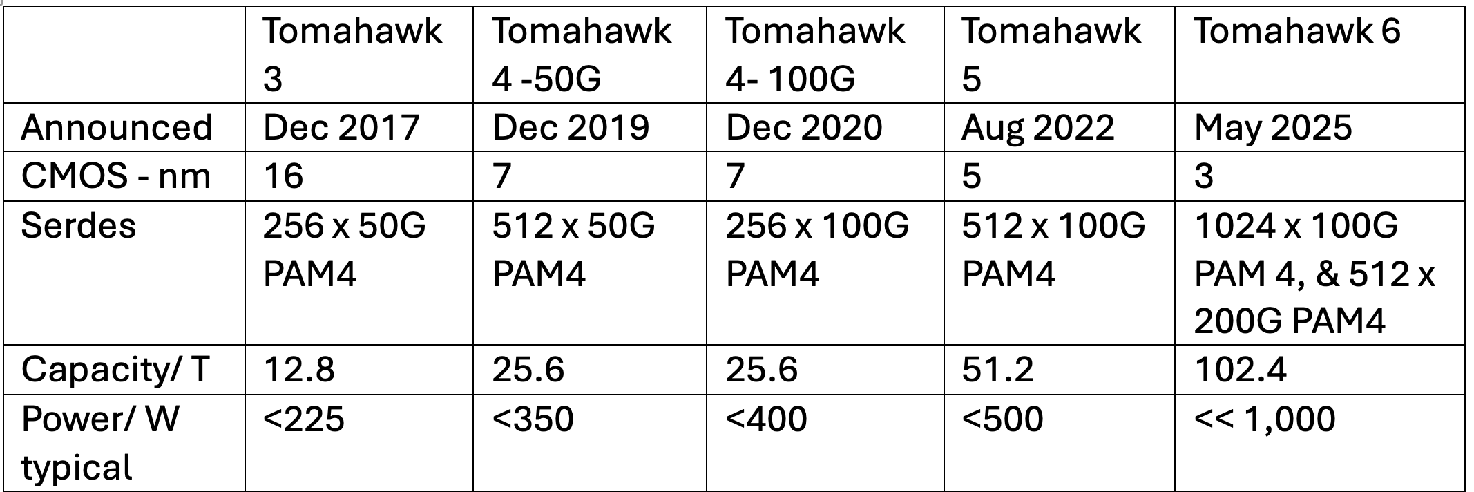
Tomahawk 6: The industry’s first 100-terabit switch chip

Part 2: Data Centre Switching
Peter Del Vecchio, product manager for the Tomahawk switch family at Broadcom, outlines the role of the company’s latest Tomahawk 6 Ethernet switch chip in AI data centres.
Broadcom is now shipping samples of its Tomahawk 6, the industry’s first 102.4-terabit-per-second (Tbps) Ethernet switch chip. The chip highlights AI’s impact on Ethernet networking switch chip design since Broadcom launched its current leading device, the 51.2-terabit Tomahawk 5. The Tomahawk 6 is more evolutionary, rather than a complete change, notes Del Vecchio. The design doubles bandwidth and includes enhanced networking features to support AI scale-up and scale-out networks.
Nvidia is the only other company that has announced a 102.4 terabit switch, and it’s scheduled for production in 2026,” says Bob Wheeler, analyst at large at market research firm LightCounting, adding that Nvidia sells switches, not chips.
Multi-die architecture
The Tomahawk 6 marks a shift from the monolithic chip design of the Tomahawk 5 to a multi-die architecture.
The 102.4 terabit Tomahawk 6 comes in two versions. One has 512 input-output lanes – serialisers/ deserialisers (serdes) – operating at 200-gigabit using 4-level pulse amplitude modulation signalling (PAM-4). The other Tomahawk 6 version has 1,024 serdes, each using 100-gigabit PAM-4.
“The core die is identical between the two, the only difference are the chiplets that are either for 100 gig or 200 gig PAM-4,” says Del Vecchio. The core die hosts the packet processing and traffic management logic.
The chip uses a 3nm CMOS process node, which improves power efficiency compared to the 5nm CMOS Tomahawk 5.
Broadcom does not quote exact power figures for the chip. “The Tomahawk 6 is significantly less than one watt per 100 gigabits-per-second, well below 1,000 watts,” says Del Vecchio. In contrast, the Tomahawk 5 consumes less than 512 watts.
AI networking: Endpoint-scheduled fabrics
The Tomahawk 6 chip is designed for AI clusters requiring near-100 per cent network utilisation.
“With previous data centre networks, it was unusual that the networks would be loaded to more than 60 to 70 per cent utilisation,” says Del Vecchio. “For AI, that’s unacceptable.”
The chip supports endpoint-scheduled fabrics, where traffic scheduling and load balancing occur at the endpoints to ensure the traffic is efficiently distributed across the network. An endpoint could be a network interface card (NIC) or an AI accelerator interface.
This contrasts with Broadcom’s other switch chip family, the Jericho 3-AI and the Ramon, which is designed for switch-scheduled fabrics. Here, the switch chip handles the networking and packet spraying, working alongside simpler end-point hardware.
The type of switch chip used – endpoint schedule or switch scheduled – depends on the preferences of service providers and hyperscalers. Broadcom says there is demand for both networking approaches.
The Tomahawk 6 uses Broadcom’s latest cognitive routing suite and enhanced telemetry to address the evolving AI traffic patterns.
The market shifted dramatically in 2022, says Del Vecchio, with demand moving from general data centre networking to one focused on AI’s needs. The trigger was the generative AI surge caused by the emergence of ChatGPT in November 2022, after the Tomahawk 5 was already shipping.
“There was some thought of AI training and for inference [with the Tomahawk 5], but the primary use case at that point was thought to be general data centre networks,” says Del Vecchio.
Wide and flat topologies
Tomahawk 6 supports two-tier networks connecting up to 128,000 AI accelerator chips, such as graphic processor units (GPUs). This assumes 200 gigabits per endpoint, which may be insufficient for the I/O requirements of the latest AI accelerator chips.
To achieve higher bandwidth per end-point – 800 gigabit or 1.6 terabit – multiple network planes are used in parallel, each adding 200 gigabits. This way, Broadcom’s design avoids adding an extra third tier of network switching.
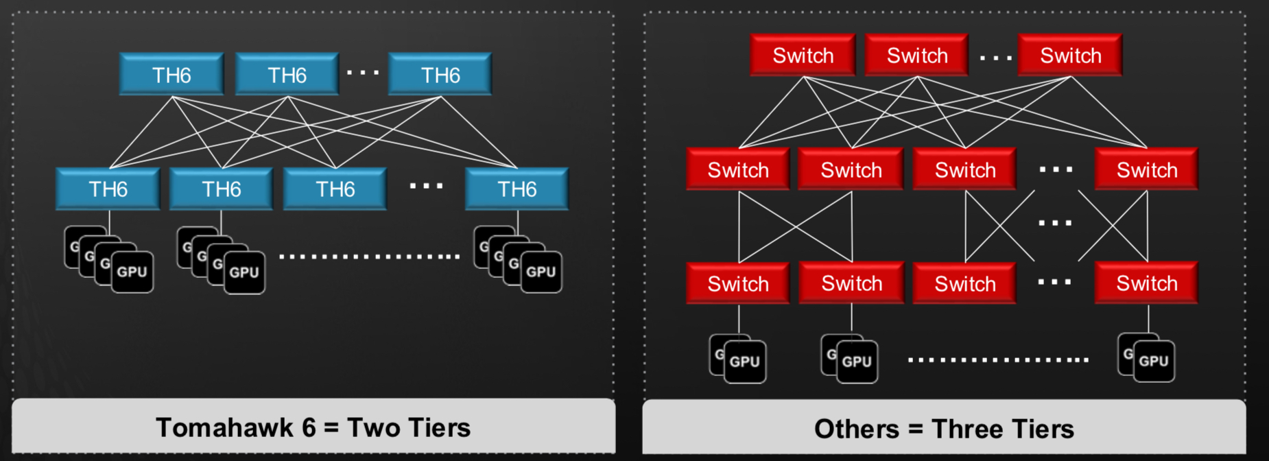
“Rather than having three tiers, you have multiple networking planes, say, eight of those in parallel,” says Del Vecchio.Such a wide-and-flat topology minimises latency and simplifies congestion control, which is critical for AI workloads. “Having a two-tier network versus a three-tier network makes congestion control much easier,” he says.
Tomahawk 6’s enhanced adaptive routing and load balancing features caters to AI’s high-utilisation demands. The aim is to try to keep the port speed low, to maximise the radix, says Del Vecchio, contrasting AI networks with general data centres, where higher 800-gigabit port speeds are typical.
Scale-Up Ethernet
The above discussion refers to the scale-out networking approach. For scale-up networking, the first hop between the AI accelerator chips, the devices are densely interconnected using multiple lanes — four or eight 200-gigabit lanes — to achieve higher bandwidth within a rack.
Broadcom has taken a different approach to scale-up networking than other companies. It has chosen Ethernet rather than developing a proprietary interface like Nvidia’s NVlink or the industry-backed UALink.
Broadcom has released its Scale-Up Ethernet (SUE) framework, which positions Ethernet as a unified solution for scale-up networks and which it has contributed to the Open Compute Project (OCP).

SUE supports large-scale GPU clusters. “You can do 512 XPUs in a scale-up cluster, connected in a single hop,” says Del Vecchio. SUE’s features include link-level retry, credit-based flow control, and optimised headers for low-latency, reliable transport.
“There is no one-size-fits-all for scale-up,” says Wheeler. “For example, Google’s ICI [inter chip interconnect] is a remote direct memory access (RDMA) based interconnect, more like Ethernet than UALink or NVLink,” says Wheeler. “There will likely be multiple camps.”
Broadcom chose Ethernet for several reasons. “One is you can leverage the whole Ethernet ecosystem,” says Del Vecchio, who stresses it results in a unified toolset for front-end, back-end, and scale-up networks.
SUE also aligns with hyperscaler preferences for interchangeable interfaces. “They’d like to have one unified technology for all that,” says Del Vecchio.
Del Vecchio is also a Ultra Ethernet Consortium (UEC) steering committee member. The UEC focuses on scale-out for its 1.0 specification, which is set for public release soon.
Link-level retry (LLR) and credit-based flow control (CBFC) are already being standardised within UEC, says Del Vecchio, and suggests that there will also be scale-up extensions which will benefit Broadcom’s SUE approach.
Interconnects
Tomahawk 6 supports diverse physical interconnects, including 100-gigabit and 200-gigabit PAM-4 serdes and passive copper links up to 2 meters, enabling custom GPU cluster designs.

“There’s a lot of focus on these custom GPU racks,” says Del Vecchio, highlighting the shift from generic pizza-box switches to highly engineered topologies.
The goal is to increase the power to each rack to cram more AI accelerator chips, thereby increasing the degree of scale-up using copper interconnect. Copper links could be used to connect two racks to further double scale-up capacity.
Co-packaged optics: Enhancing reliability?
Co-packaged optics (CPO) has also become a design feature of switch chips. The Tomahawk 6 will be Broadcom’s third-generation switch chip that will also be offered with co-packaged optics.
“People are seeing how much power is going into the optics for these GPU racks,” says Del Vecchio. Co-packaged optics eliminates retimers and DSPs, reducing latency and burst errors
Broadcom and hyperscalers are currently investigating another key potential benefit of co-packaged optics. “There are indications that you wind up with significantly fewer link flaps,” he said. A link flap refers to an link instability.
Unlike pluggable optics, which introduce burst errors via DSPs, co-packaged optics offers random Gaussian noise, which is better suited for forward error correction schemes. “If you have an end-to-end CPO link, you have much more random errors,” he explained.
This suggests that using co-packaged optics could benefit the overall runtime of massive AI clusters, a notable development that, if proven, will favour the technology’s use. “We expect the Tomahawk 6 Davisson co-packaged optics version to follow Tomahawk 6 production closely,” says LightCounting’s Wheeler.
Design challenges
Tomahawk 6’s development required overcoming significant hurdles.
Packaging over 1,000 serdes was one. “There were no packages on the market anywhere near that size,” says Del Vecchio, emphasising innovations in controlling warpage, insertion loss, and signal integrity. Del Vecchio also highlights the complexity of fanning out 1,000 lanes. The multi-die design required low-latency, low-power chip-to-chip interfaces, with Broadcom using its experience developing custom ASICs.
Traffic management structures, like the Memory Management Unit (MMU), have also seen exponential complexity increases. “Some structures are 4x the complexity,” says Del Vecchio.
The multi-die design demanded efficient chip-to-chip interfaces, while packaging 1,000 serdes lanes required signal integrity and manufacturability innovations. “We spent a lot of time on the packaging technology,” he added.
Meanwhile, using architectural optimisations, such as automatic clock gating and efficient serdes design, improved power efficiency. What about the delay in announcing the latest Tomahawk switch chip compared to the clock-like 2-year launch date gaps of previous Tomahawk chips? (See table above.)
Del Vecchio says the delay wasn’t due to a technical issue or getting access to a 3nm CMOS process. Instead, choosing the right market timing drove the release schedule.
Broadcom believes it has a six-month to one-year lead on competing switch chip makers.
Production and market timing
Tomahawk 6 samples are now shipping to hyperscalers and original equipment manufacturers (OEMs). Production is expected within seven months, matching the timeline achieved with the Tomahawk 5. “We feel confident there is no issue with physical IP,” says Del Vecchio, based on the work done with Broadcom’s test chips and verification suites.
The simultaneous availability of 100-gigabit and 200-gigabit SerDes versions of the latest switch chip reflects AI’s bandwidth demands.
“There is such a huge insatiable demand for bandwidth, we could not afford the time delay between the 100-gig and 200-gig versions,” says Del Vecchio.

Broadcom’s silicon for the PCI Express 6.0 era
Broadcom has detailed its first silicon for the sixth generation of the PCI Express (PCIe 6.0) bus, developed with AI servers in mind.
The two types of PCIe 6.0 devices are a switch chip and a retimer.
Broadcom, working with Teledyne LeCroy, is also making available an interoperability development platform to aid engineers adopting the PCIe 6.0 standard as part of their systems.
Compute servers for AI are placing new demands on the PCIe bus. The standard no longer about connects CPUs to peripherals but also serving the communication needs of AI accelerator chips.
“AI servers have become a lot more complicated, and connectivity is now very important,” says Sreenivas Bagalkote, Broadcom’s product line manager for the data center solutions group.
Bagalkote describes Broadcom’s PCIe 6.0 switches as a ‘fabric’ rather than silicon to switch between PCIe lanes.
PCI Express
PCIe is an long-standing standard adopted widely, not only for computing and servers but across industries such as medical imaging, automotive, and storage.
The first three generations of PCIe evolved around the CPU. There followed a big wait for the PCIe 4.0, but since then, a new PCI generation has appeared every two years, each time doubling the data transfer rate.
Now, PCIe 6.0 silicon is coming to the market while work continues to progress on the latest PCIe 7.0, with the final draft ready for member review.
The PCIe standard supports various lane configurations from two to 32 lanes. For servers, 8-lane and 16-lane configurations are common.
“Of all the transitions in PCIe technology, generation 6.0 is the most important and most complicated,” says Bagalkote.
PCIe 6.0 introduces several new features. Like previous generations, it doubles the lane rate: PCIe 5.0 supports 32 giga-transfers a second (GT/s) while PCIe 6.0 supports 64GT/s.
The 64GT/s line rate requires the use of 4-level pulse amplitude modulation (PAM-4) for the first time; all previous PCIe generations use non-return-to-zero (NRZ) signalling.
Since PCIe must be backwards compatible, the PCIe 6.0 switch supports PAM-4 and NRZ signalling. More sophisticated circuitry is thus required at each end of the link as well as a forward error correction scheme, also a first for the PCIe 6.0 implementation.
Another new feature is flow control unit (FLIT) encoding, a network packet scheme designed to simplify data transfers.
PCIe 6.0 also adds integrity and data encryption (IDE) to secure the data on the PCIe links.
AI servers
A typical AI server includes CPUs, 8 or 16 interconnect GPUs (AI accelerators), network interface cards (NICs) to connect to GPUs making up the cluster, and to storage elements.
A typical server connectivity tray will likely have four switch chips, one for each pair of GPUs, says Bagalkote. Each GPU has a dedicated NIC, typically with a 400 gigabit per second (Gbps) interface. The PCIe switch chips also connect the CPUs and NVMe storage.
Broadcom’s existing generation PCIe 5.0 switch ICs have been used in over 400 AI server designs, estimated by the company at 80 to 90 per cent of all deployed AI servers.
Switch and retimer chips
PCIe 6.0’s doubling the lane data rate makes sending signals over 15-inch rack servers harder.
Broadcom says its switch chip uses serialiser-deserialiser (serdes) that outperform the PCIe specification by 4 decibels (dB). If an extra link distance is needed, Broadcom also offers its PCIe 6.0 retimer chips that also offer an extra 4dB.
Using Broadcom’s ICs at both ends results in a 40dB link budget, whereas the specification only calls for 32dB. “This [extra link budget] allows designers to either achieve a longer reach or use cheaper PCB materials,” says Bagalkote.
The PCIe switch chip also features added telemetry and diagnostic features. Given the cost of GPUs, such features help data centre operators identify and remedy issues they have, to avoid taking the server offline
“PCIe has become an important tool for diagnosing in real-time, remotely, and with less human intervention, all the issues that happen in AI servers,” says Bagalkote.
Early PCIe switches were used in a tree-like arrangement with one input – the root complex – connected via the switch to multiple end-points. Now, with AI servers, many devices connect to each other. Broadcom’s largest device – the PEX90144 – can switches between its 144 PCIe 6.0 lanes while supporting 2-, 4-, 8- or 16-lane-wide ports.
Broadcom also has announced other switch IC configurations with 104- and 88-lanes. These will be followed by 64 and 32 lane versions. All the switch chips are implemented using a 5nm CMOS process.
Broadcom is shipping “significant numbers” of samples of the chips to certain system developers.
PCIe versus proprietary interconnects
Nvidia and AMD that develop CPUs and AI accelerators have developed their own proprietary scale-up architectures. Nvidia has NVLink, while AMD has developed the Infinity Fabric interconnect technology.
Such proprietary interconnect schemes are used in preference to PCIe to connect GPUs, and CPUs and GPUs. However, the two vendors use PCIe in their systems to connect to storage, for example.
Broadcom says that for the market in general, open systems have a history of supplanting closed, proprietary systems. It points to the the success of its PCIe 4.0 and PCIe 5.0 switch chips and believes PCIe 6.0 will be no different.
Disaggregated system vendor developer, Drut Technologies, is now shipping a PCIe 5.0-based scalable AI cluster that can support different vendors’ AI accelerators. Its system uses Broadcom’s 144-lane PCIe 5.0 switch silicon for its interconnect fabric.
Drut is working on its next-generation PCIe 6.0-generation-based design.

ECOC 2024 industry reflections
Gazettabyte is asking industry figures for their thoughts after attending the recent 50th-anniversary ECOC show in Frankfurt. Here are the first contributions from Huawei's Maxim Kuschnerov, Coherent's Vipul Bhatt, and Broadcom's Rajiv Pancholy.
Maxim Kuschnerov, Director R&D, Optical & Quantum Communication Laboratory at Huawei.
At ECOC, my main interest concerned the evolution of data centre networking to 400 gigabits per lane for optics and electronics. Historically, the adoption of new optical line rates always preceded the serdes electrical interconnects but now copper cables are likely to drive much of the leading development work at 400 gigabit per lane.
Arista Networks argued that 448G-PAM6 works better for copper, while 448G-PAM4 is the better choice for optics – a recurring argument. While PAM6 signalling is certainly more suitable for longer copper cables, it will face even tougher challenges on the optical side with increasing reflection requirements in newly built, dusty data centres. Also, a linear drive option for future Ethernet will be imperative, given the DSP’s increasing share of the the consumption in pluggable modules. Here, a native 448G-PAM4 format for the serdes (the attachment unit interface or AUI) and optics looks more practical.
My most important takeaway regarding components was the initial feasibility of electro-absorption modulated lasers (EMLs) with a greater than 100GHz analogue bandwidth, presented by Lumentum and Mitsubishi publicly and other companies privately. Along with thin-film lithium niobate (TFLN) Mach–Zehnder modulators suited for Direct Reach (DR) applications with shared lasers, EMLs have historically offered low cost, small size and native laser integration.
For 1.6-terabit modules, everyone is waiting on the system availability of 224-gigabit serdes at a switch and network interface card (NIC) level. The power consumption of 1.6-terabit optical modules will improve with 3nm CMOS DSPs and native 200 gigabit per lane. Still, it gets into an unhealthy region where the network cable power consumption is in the same ballpark as the system function of switching. Here, the bet on LPO certainly didn’t pay off at 100 gigabits per lane and will not pay off at 200 gigabits per lane at scale. The question is whether linear receive optics (LRO)/ half-retimed approaches will enter the market. Technically, it’s feasible. So, it might take one big market player with enough vertical integration capability and a need to reduce power consumption to move the needle into this more proprietary, closed-system direction. Nvidia showcased their PAM4 DSP at the show. Just saying…
212G VCSELs are still uncertain. There is a tight initial deployment window to be hit if these high-speed VCSELS are to displace single-mode fibre-based optics at the major operators. Coherent’s results of 34GHz bandwidth are not sufficient and don’t look like something that could yet be produced at scale. Claims by some companies that a 400 gigabit per lane VCSEL is feasible sound hollow for now, with the industry crawling around the 30GHz bandwidth window.
Last but not least, co-packaged optics. For years, this technology couldn’t escape gimmick status. Certainly, reliability, serviceability, and testability of co-packaged optics using today’s methodology would make a deployment impractical. However, the big prize at 400 gigabit per lane is saving power – a significant operational expense for operators – something that is too attractive to ignore.
The targets of improving optics diagnostics, developing higher-performance dust-reflection DSP algorithms to deal with multi-path interference, adopting more resiliency to failure in the network, and introducing a higher degree of laser sparing are not insurmountable tasks if the industry sets its mind to them. Given the ludicrous goals of the AI industry, which is reactivating and rebranding nuclear power plants, a significant reduction in network power might finally serve a higher purpose than just building a plumber’s pipe.
Vipul Bhatt, Vice President of Marketing, Datacom Vertical, Coherent
ECOC 2024 was the most convincing testimony that the optical transceiver industry has risen to the challenge of AI’s explosive growth. There was hype, but I saw more solid work than hype. I saw demonstrations and presentations affirming that the 800-gigabit generation was maturing quickly, while preparations are underway for the next leap to 1.6 terabit and then 3.2 terabit.
This is no small feat, because the optics for AI is more demanding in three ways. I call them the three P’s of AI optics: performance, proliferation, and pace.
Performance because 200 gigabit PAM4 optical lanes must work with a low error rate at higher bandwidth. Proliferation because the drive to reduce power consumption has added new transceiver variants like linear packaged optics (LPO) and linear receive optics (LRO). And pace because the specifications of AI optics are evolving at a faster pace than traditional IEEE standards.
Rajiv Pancholy, Director of Hyperscale Strategy and Products, Optical Systems Division, Broadcom
As generative AI systems move to unsupervised, transformer-based parallel architectures, there is less time for resending packets due to data transmission errors. Improved bit error rates are thus required to reduce training times while higher interconnect bandwidth and data rates are needed to support larger GPU clusters. These compute networks are already moving to 224 gigabit PAM4 well before the previous generation at 112 gigabit PAM4 was allowed to reach hyperscale deployment volumes.
The problem is scalability with a high-radix supporting all-to-all connectivity. The power for a single rack of 72 GPUs is 120kW, and even with liquid cooling, this becomes challenging. Interconnecting larger scale-up and scale-out AI computing clusters requires more switching layers which increases latency.
Furthermore, after 224 gigabit PAM4, the losses through copper at 448 gigabit PAM4 make link distances from the ASIC too short. Moving to modulation schemes like PAM-6 or PAM-8 presents a problem for the optics, which would need to stay at 448 gigabit PAM4 to minimize crosstalk and insertion losses.
Supporting 448 gigabit PAM4 with optics then potentially requires new materials to be integrated into silicon, like thin-film lithium niobate (TFLN) and Barium Titanate (BaTiO3), electro-optic (EO) polymers, and III-V materials like Indium Phosphate (InP) and Gallium Arsenide (GaAs). So now we have a gearbox and, potentially, a higher forward error correction (FEC) coding gain is required, adding more power and latency before the signal even gets to the transmit-side optics.
There were 1.6-terabit OSFP transceivers operating with eight lanes of 212.5 gigabit PAM4 while vendors continue to work towards a 3.2-terabit OSFP-XD. With 32 x 3.2Tbps pluggables operating at 40W each, the optical interconnect power would be 1.3kW for a 102.4Tbps switch. And if you use 64 x 1.6Tbps OSFP at 25W each, the optical interconnect power will be eben higher, at 1.6kW. I wonder how linear pluggable optics can compensate for all the path impairments and reflections at high data rates from pluggable solutions. Perhaps you can relax link budgets, temperature requirements, and interoperability compliance.
The best session this year was the last ECOC Market Focus panel on the Tuesday, which kept everyone a bit longer before they could figure out where in Frankfurt Oktoberfest beer was on tap. The panel addressed “Next-Gen Networking Optics like 1.6T or 3.2T”. All but one of the participants discussed the need and a migration to co-packaged optics, which we at Broadcom first demonstrated in March 2022.
It was great to also present at the ECOC Market Focus forum. My presentation was titled “Will you need CPO in 3 years?” Last year in Glasgow, I gave a similar presentation: “Will you need CPO in 5 years?”

Broadcom's Thor 2 looks to hammer top spot in AI NICs
Jas Tremblay
“It [the design] gives customers choices and freedom when they’re building their AI systems such that they can use different NICs with different [Ethernet] switches,” says Tremblay.
NICs for AI
The 400GbE Thor 2 supports 16 lanes of PCI Express 5.0, each lane operating at 32 gigabit-per-second (Gbps).
The chip also features eight 112-gigabit serialisers/ deserialisers (serdes). Eight 112-gigabit serdes are supported even though the chip is a 400GbE device since some customers operate the serdes at the lower 56Gbps speed to match their switches’ serdes.
Broadcom is bringing to market a variety of NICs using the Thor 2. Tremblay explains that one board is for standard servers while another is designed for an Open Compute Project (OCP) server. In turn, certain customers have custom designs.
Broadcom has also qualified 100 optical and copper-based connectors used with the NIC boards. “People want to use different cables to connect these cards, and we have to qualify them all,” says Tremblay. These include linear pluggable optics (LPO), for the first time as part of the optical options.
The requirement for so many connectors is a reflection of several factors: AI’s needs, the use of 100-gigabit serdes, and 400GbE. “What’s happening is that customers are having to optimise the physical cabling to reduce power and thermal cooling requirements,” says Tremblay.
When connecting the Broadcom NIC to a Broadcom switch, a reach of 5m is possible using direct attach copper (DAC) cabling. In contrast, if the Broadcom NIC is connected to another vendor’s switch, the link distance may only be half that.
“In the past, people would say: ‘I’m not going to have different cable lengths for various types of NICs and switch connections’,” says Tremblay. “Now, in the AI world, they have to do that given there’s so much focus on power and cooling.”

 How the NIC connects to the accelerator chip (in the diagram, a graphics processing unit (GPU)) and also the layers of switches to enable the NIC to talk to other NICs. Source: Broadcom.
NIC categories
Many terms exist to describe NICs. Broadcom, which has been making NICs for over two decades, puts NICs into two categories. One, and Broadcom’s focus, is Ethernet NICs. The NICs use a hardware-accelerated data path and are optimised for networking, connectivity, security, and RoCE.
RoCE refers to RDMA over Converged Ethernet, while RDMA is short for remote direct memory access. RDMA allows one processor to read or write to another’s memory without involving the processor. This frees the processor to concentrate on computation. RoCE uses Ethernet as a low-latency medium for such transfers.
The second NIC category refers to a data processing unit (DPU). Here, the chip has CPU cores to execute the offload tasks, implementing functions that would otherwise burden the main processor.
Tremblay says the key features that make an Ethernet NIC ideal for AI include using at least a 25Gbps serdes, RoCE, and advanced traffic congestion control.
Switch scheduling or end-point scheduling
Customers no longer buy components but complete AI compute clusters, says Tremblay. They want the cluster to be an open design so that when choosing the particular system elements, they have confidence it will work.
Broadcom cites two approaches – switch scheduling and end-point scheduling – to building AI systems.
Switch scheduling refers to systems where the switch performs the traffic load balancing to ensure that the networking fabric is used to the full. The switch also oversees congestion control.
 Hasan Siraj
“The switch does perfect load balancing with every packet spread across all the outbound lines and reassembled at the other end,” says Hasan Siraj, head of software products and ecosystem at Broadcom. Jericho3-AI, which Broadcom announced last year, is an example of a switch scheduler for AI workloads.
The second approach – end-point scheduling – is for customers that prefer the NIC to do the scheduling. Leading cloud-computing players have their own congestion control algorithms, typically, and favour such flexibility, says Siraj: “But you still need a high-performance fabric that can assist with the load balancing.”
Here, a cloud player will used their NIC designs or other non-Broadcom NICs for the congestion control control but use it with a Broadcom switch such as the Tomahawk 5 (see diagram below).
 Left shows an end-point scheduler set-up while the right diagram is an example of switch scheduler. Source: Broadcom.
Accordingly, the main configuration options are a Broadcom NIC with a non-Broadcom switch, a third-party NIC and the Jericho3-AI, or a full NIC-switch Broadcom solution where the Jericho3-AI does the load balancing and congestion control, while the Thor 2-based NIC takes care of RoCE in a power efficient way.
“Our strategy is to be the most open solution,” says Tremblay. “Everything we are doing is standards-based.”
And that includes the work of the Ultra Ethernet Consortium that is focussed on transportation and congestion control to tailor Ethernet for AI. The Ultra Ethernet Consortium is close to issuing the first revisions of its work.
The Ultra Ethernet Consortium aspires to achieve AI cluster sizes of 1 million accelerator chips. Such a huge computing cluster will not fit within one data centre sue to size, power, and thermal constraints, says Siraj. Instead, the cluster will be distributed across several data centres tens of kilometres apart. The challenge here will be how to achieve such connectivity while maintaining job completion time and latency.
Thor 3
Meanwhile, Broadcom has started work on an 800-gigabit NIC chip, the Thor 3, and a 1.6-terabit version after that.
The Jericho3-AI switch chip supports up to 32,000 endpoints, each at 800Gbps. Thus, the AI switch chip is ready for the advent Thor 3-based NIC boards.

Teramount’s scalable fibre-attach for co-packaged optics
 Part 2: Co-packaged optics: fibre-attach
Hesham Taha recently returned from a trip to the US to meet with leading vendors and players serving the silicon photonics industry.
“It is important to continue probing the industry,” says Taha, the CEO of start-up Teramount.
Teramount specialises in fibre assembly technology: coupling fibre to silicon photonics chips.
Taha is now back in the US, this time to unveil Teramount’s latest product at this week’s OFC show being held in San Diego. The company is detailing a new version of its fibre assembly technology, dubbed Teraverse-XD, that doubles the density of fibres connected to a silicon photonics chip.
Teramount is also announcing it is working with GlobalFoundries, a leading silicon-photonics foundry.
Connecting fibre to a silicon photonics device for a pluggable optical module is straightforward. However, attaching fibre to an optical engine for co-packaged optics is challenging. The coupling must be compact and scale to enable even denser connections in future. This is especially true with the co-packaging of future 100-terabit and 200-terabit Ethernet switch chips.
“If I were to describe the last year, it would be aligning our [Teramount] activities to the industry’s evolving needs,” says Taha. “A key part of those needs is being driven by optical activities for AI applications.”
Edge versus surface coupling
Companies are pursuing two main approaches to connecting fibre to a silicon photonics device: surface and edge (side) coupling.
Surface coupling – or its academic term, off-plane coupling – deflects light vertically, away from the chip’s surface. In contrast, edge (in-plane) or side coupling sends the optical waveguide’s light straight through to the fibre at the chip’s edge.
A silicon-photonics grating coupler is used for surface coupling, glancing the light away from the chip’s plane. However, the grating coupler is wavelength-dependent such that the angle of the defection varies with the light.
In contrast, side coupling is wideband. “You can carry multiple wavelengths on each channel,” says Taha. However, side coupling has limited interfacing space, referred to as ‘shoreline density’.
Side coupling is also more complicated to manufacture in volume. Directly bonding the fibre to the chip involves adhesive, and the fibres get in the way of reflow soldering. “It [side coupling] is doable for transceivers, but to make co-packaged optics, side coupling becomes complicated,” says Taha.
Teramount’s approach
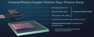
Teramount’s approach couples the fibre to the silicon photonics chip using two components: a photonic plug and a photonic bump.
The photonic plug holds the fibres and couples them to the silicon photonics chip via the photonic bump, a component made during the silicon photonics wafer processing. The photonic bump consists of two elements: a wideband deflector and a lens mirror for beam expansion. Expanding the light beam enables much larger assembly tolerances: +/- 30 microns. And across this 60-micron window, only half a dB is lost in misalignment tolerances.
The resulting wafer-level manufacturing may be more complicated, says Taha, but the benefit is relaxed tolerances in the assembly, wide-band surface coupling, and when testing the wafer and the die.
The photonic bump-and-plug combination also enable detachable optics for co-packaged optics designs. This benefits manufacturing and is wanted for co-packaged optics.
Teraverse and Teraverse-XD
There is a clear demarcation between the optics and the switch chip when using pluggables in the data centre. In contrast, co-packaged optics is a system with the optics embedded alongside the chip. A vendor may work with multiple companies to make co-packaged optics, but one product results, with the chip and optical engined co-packaged.
Teramount’s Teraverse solution, using the plug-and-bump combination, brings pluggability to co-packaged optics. The fibres can be attached and detached from the optical engines. “It’s very important to keep that level of pluggability for co-packaged optics,” says Taha.
The approach also benefits manufacturing yield and testing. Separating the fibres from the package protects the fibres during reflow soldering. “Ideally, you want the fibre connected at the last stage and still maintain high level of testability during the packaging process,” says Taha.
Detachable fibre also brings serviceability to co-packaged optics, benefitting for data centre operators.
Teraverse, Teramount’s detachable fiber-to-chip interface, supports single-mode fiber with 125-micron diameter at a 127-micron pitch separation.

Teraverse-XD, announced for OFC, is a follow-on that doubles the fibre density to achieve a near 64-micron pitch. Here, fibres are placed on top of each other, scaling in the Z-dimension. The approach is like how rods or pipes are stored, with the second row of fibres staggered, sitting in the valleys between adjacent fibers in the lower row.
Two rows of photonic bumps are used to couple the light to each row of fibres (see image above). “It’s very important to keep the same real-estate but to have twice the number of fibres,” says Taha.
Future scaling is possible by adding more rows of fibres or by adopting fibres with a smaller pitch.
Teramount’s technology also supports both edge coupling and surface coupling. “We are agnostic,” says Taha. If a co-packaged optics or optical engine vendor wants to use side coupling, it can use the bump-and-plug combination. The bump deflects the beam upwards to the plug packaging which takes the fibres and sends them out horizontally. “We are converting edge coupling to wideband surface coupling,” says Taha. “You don’t need to sacrifice bandwidth to do surface coupling.”
If the vendor wishes to use a grating coupler, Teramount’s bump-and-plug supports that, too, enabling detachable fibering. But here, only the bump’s expanding mirror is used. “For the wideband surface coupling cased, the bump uses two components: the deflector and the expanding mirror,” says Taha.
Both cases are supported by what Teramount refers to as its Universal Photonic Coupler, shown.
Market expectations
Despite being discussed for over a decade, Taha is not surprised that data centre operators have yet to adopt co-packaged optics.
He points out that hyperscalers only want to use co-packaged optics for Ethernet switches once the technology is more mature. They can also keep using a proven alternative: pluggable modules, that continue to advance.
“Hyperscalers are not against the technology, but it is not mature enough,” says Taha. Hyperscalers and systems vendors also want an established supply chain and not proprietary solutions.
To date, Broadcom’s first co-packaged optics switch solution at 25.6-terabit was adopted by Tencent. Broadcom has announced for OFC that it is now delivering its latest 51.2-terabit Bailly co-packaged optics design, backed by ByteDance.
“AI is a different story,” says Taha. “This is the tipping point for a leading vendor to start taking seriously co-packaged optics.”
The advantage of co-packaged optics here is that it accommodates the reach – radix -as well as power savings and improved latency.
Taha expects initial volumes of co-packaged optics sales in 2026.

Broadcoms taps AI to improve switch chip traffic analysis
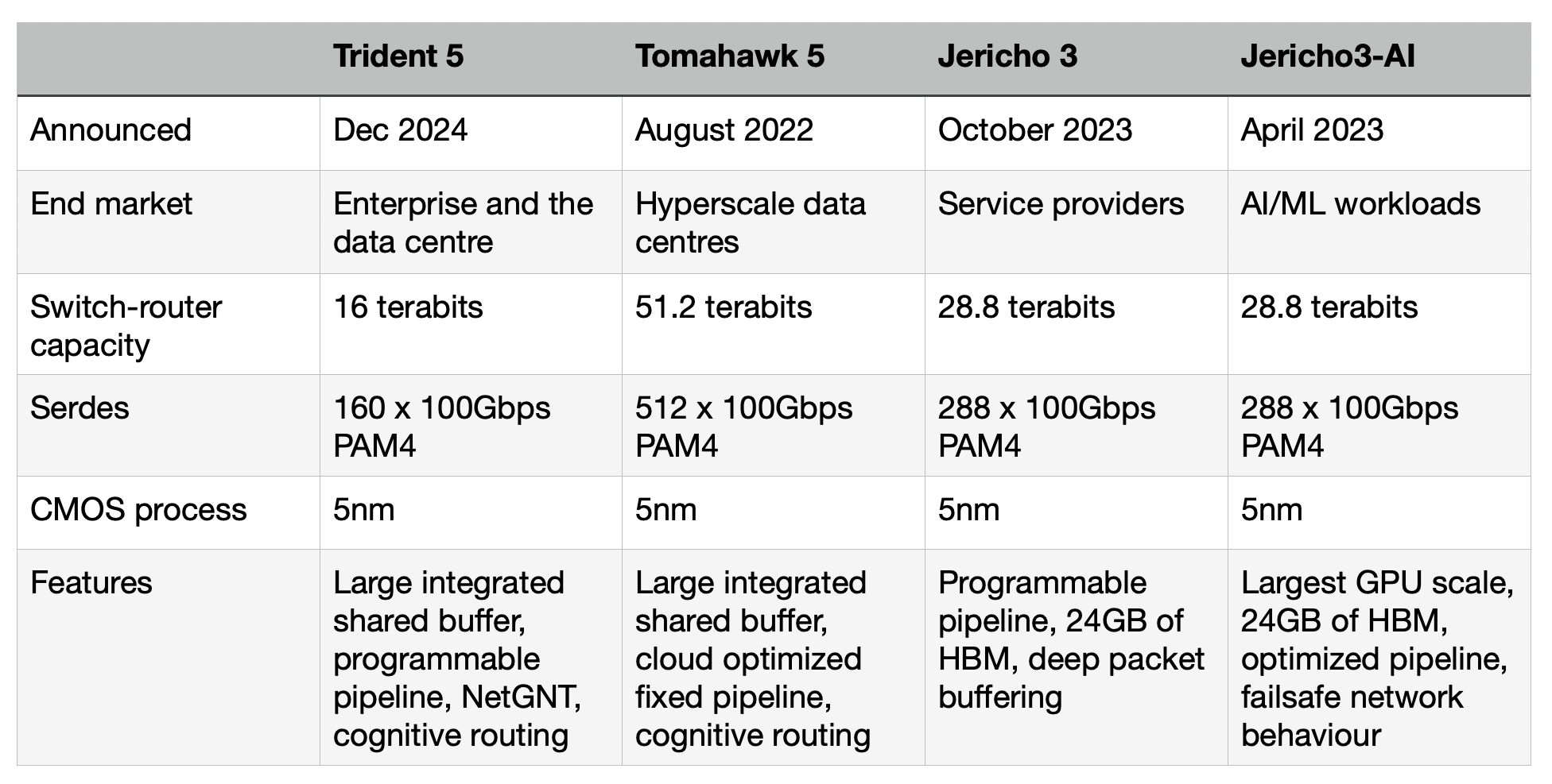
Broadcom’s Trident 5-X12 networking chip is the company’s first to add an artificial intelligence (AI) inferencing engine.
Data centre operators can use their network traffic to train the chip’s neural network. The Trident 5’s inference engine, dubbed the Networking General-purpose Neural-network Traffic-analyzer or NetGNT, is loaded with the resulting trained model to classify traffic and detect security threats.
“It is the first time we have put a neural network focused on traffic analysis into a chip,” says Robin Grindley, principal product line manager with Broadcom’s Core Switching Group.
Adding an inference engine shows how AI can complement traditional computation, in this case, packet processing.
Trident family
Trident is one of Broadcom’s main three lines of networking and switch chips, the Jericho and Tomahawk being the other two.
Service providers favour the Jericho family for high-end IP routing applications. The Ethernet switch router chip’s features include a programmable pipeline and off-chip store for large traffic buffering and look-up tables.
The latest Jericho 3, the 28.8 terabits-per-sec (Tbps) Jericho 3, was announced in September. Broadcom launched the first family device, the Jericho3-AI, earlier this year; a chip tailored for AI networking requirements.
In contrast, Broadcom’s Tomahawk Ethernet network switch family addresses the data centre operators’ needs. The Tomahawk has a relatively simple fixed packet-processing pipeline to deliver the highest switching capacity. The Tomahawk 5 has a capacity of 51.2 terabits and includes 512, 100-gigabit PAM4 serialiser-deserializer (serdes).
“The big hyperscalers want maximum bandwidth and maximum radix [switches],” says Grindley. “The hyperscalers have a pretty simple fabric network and do everything else themselves.”
The third family, the Trident Ethernet switch chips, is popular for enterprise applications. Like the Jericho, the Trident has a programmable pipeline to address enterprise networking tasks such as Virtual Extensible LAN (VXLAN), tunnelling protocols, and segment routing (SRv6).
The speeds and timelines of the various Tomahawk and Trident chips are shown in the chart.

Trident 5-X12
The Trident 5-X12 is implemented using a 5nm CMOS process and has a capacity of 16 terabits. The chip’s input-output includes 160, 100-gigabit PAM4 serdes. These are the serdes that Broadcom introduced with the Tomahawk 5.
The first chip of each new generation of Trident usually has the highest capacity and is followed by lower-capacity devices tailored to particular markets.
Trident 5 is aimed at top-of-rack switch applications. Typically, 24 or 48 ports of the top-of-rack switch are used for downlinks to connect to servers, while 4 or 8 are used for higher-capacity uplinks (see diagram).
The Trident 5 can support 48 ports of 200 gigabits for the downlinks and eight 800 gigabit for the uplinks. To support 800-gigabit interfaces, the chip uses eight 100-gigabit serdes and an one-chip 800-gigabit media access controller (MAC). Other top-of-rack switch configurations are shown in the diagram.
Currently, 400-gigabit network interface cards are used for demanding applications such as machine learning. Trident5 is also ready to transition to 800-gigabit network interface cards.
Another Tomahawk feature the Trident 5 has adopted is cognitive routing, a collection of congestion management techniques for demanding machine-learning workloads.
One of the techniques is global load balancing. Previous Trident devices supported dynamic load balancing, where the hardware could see the congested port and adapt in real-time. However, such a technique gives no insight into what happens further along the flow path. “If I knew that, downstream, somebody else was congested, then I could make a smarter decision,” says Grindley. Global load balancing does just this. It sends notification to the routing chips upstream that there is congestion so they can all work together.
Another cognitive routing feature is drop congestion notification. Here, packets dropped due to congestion are captured such that what is sent is only their header data and where the packet was dropped. This mechanism improves flow completion times compared to normal packet loss, which is costly for machine-learning workloads.
Trident 5, like its predecessor, Trident 4, has a heterogeneous pipeline of tile types. The tiles contain static random-access memory (SRAM), ternary content-addressable memory (TCAM) or arithmetic logic units. The tiles allow multiple look-ups or actions in parallel at each stage in the pipeline.

Broadcom has a compiler that maps high-level packet-processing functions to its pipeline in the NPL programming language. The latency through the device stays constant, however the packet processing is changed, says Grindley.
Trident 5’s NetGNT inference engine is a new pipeline resource for higher-level traffic patterns. “NexGNT looks at things not at a packet-by-packet level, but across time and the overall packet flow through the network,” says Grindley.
The NetGNT
Until now system architects and network operation centre staff have defined a set of static rules written in software to uncover and treat suspicious packet flows. “A pre-coded set of rules is limited in its ability to catch higher-level traffic patterns,” says Grindley.
When Broadcom started the Trident 5 design, its engineers thought a neural network approach could be used. “We knew it would be useful if you had something that looked at a higher level, and we knew neural networks could do this kind of task,” says Grindley.
The neural network sits alongside the existing traffic analysis logic. Information such as packet headers, or data already monitored and generated by the pipeline, can be fed to the neural network to assess the traffic patterns.
“It sits there and looks for high-level patterns such as the start of a denial of service attack” says Grindley.
Training
The neural network is trained using supervised learning. A human expert must create the required training data and train the model using supervised learning. The result is a set of weights loaded onto the Trident 5’s neural network.

When the neural network is triggered, i.e. when it identifies a pattern of interest, the Trident 5 must decide what it should do. The chip can drop the packets or change the quality of service (QoS). The device can also drop a packet while creating a mirror packet containing headers and metadata. This can then be sent to a central analyser at the network operations centre to perform higher-level management algorithms.
Performance
The Trident 5 chip is now sampling. Broadcom says there is no performance data as end customers are still to train and run live traffic through the Trident 5’s inference engine.
“What it can do for them depends on getting good data and then running the training,” says Grindley. “Nobody has done this yet.”
Will the inference engine be used in other Broadcom networking chips?
“It depends on the market,” says Grindley. “We can replicate it, just like taking IP from the Tomahawk where appropriate.”

ECOC 2023 industry reflections - Part 3

Gazettabyte is asking industry figures for their thoughts after attending the recent ECOC show in Glasgow. In particular, what developments and trends they noted, what they learned and what, if anything, surprised them. Here are responses from Coherent, Ciena, Marvell, Pilot Photonics, and Broadcom.
Julie Eng, CTO of Coherent
It had been several years since I’d been to ECOC. Because of my background in the industry, with the majority of my career in data communications, I was pleasantly surprised to see that ECOC had transitioned from primarily telecommunications, and largely academic, into more industry participation, a much bigger exhibition, and a focus on datacom and telecom. There were many exciting talks and demos, but I don’t think there were too many surprises.
In datacom, the focus, not surprisingly, was on architectures and implementations to support artificial intelligence (AI). The dramatic growth of AI, the massive computing time, and the network interconnect required to train models are driving innovation in fibre optic transceivers and components.
There was significant discussion about using Ethernet for AI compared to protocols such as InfiniBand and NVLink. For us as a transceiver vendor, the distinction doesn’t have a significant impact as there is little if any, difference in the transceivers we make for Ethernet compared to the transceivers we make for InfiniBand/NVLink. However, the impact on the switch chip market and the broader industry are significant, and it will be interesting to see how this evolves.
Linear pluggable optics (LPO) was a hot topic, as it was at OFC 2023, and multiple companies, including Coherent, demonstrated 100 gigabit-per-lane LPO. The implementation has pros and cons, and we may find ourselves in a split ecosystem, with some customers preferring LPO and others preferring traditional pluggable optics with DSP inside the module. The discussion is now moving to the feasibility of 200 gigabit-per-lane LPO.
Discussion and demonstrations of co-packaged optics also continued, with switch vendors starting to show Ethernet switches with co-packaged optics. Interestingly, the success of LPO may push out the implementation of co-packaged optics, as LPO realizes some of the advantages of co-packaged optics with a much less dramatic architectural change.
One telecom trend was the transition to 800-gigabit digital coherent optical modules, as customers and suppliers plan for and demonstrate the capability to make this next step. There was also significant interest in and discussion about 100G ZR. We demonstrated a new version with 0dBm high optical output power at ECOC 2023 while other companies showed components to support it. This is interesting for cable providers and potentially for data centre interconnect and mobile fronthaul and backhaul.
I was very proud that our 200 gigabit-per-lane InP-based DFB-MZ laser won the 2023 ECOC Exhibition Industry Award for Most Innovative Product in the category of Innovative Photonics Component.
ECOC was a vibrant conference and exhibition, and I was pleased to attend and participate again.
Loudon Blair, senior director, corporate strategy, Ciena
ECOC 2023 in Glasgow gave me an excellent perspective on the future of optical technology. In the exhibition, integrated photonic solutions, high-speed coherent pluggable optical modules, and an array of testing and interoperability solutions were on display.
I was especially impressed by how high-bandwidth optics is being considered beyond traditional networking. Evolving use cases include optical cabling, the radio access network (RAN), broadband access, data centre fabrics, and quantum solutions. The role of optical connectivity is expanding.
In the conference, questions and conversations revolved around how we solve challenges created by the expanding use cases. How do we accommodate continued exponential traffic growth on our fibre infrastructure? Coherent optics supports 1.6Tbps today. How many more generations of coherent can we build before we move on to a different paradigm? How do we maximize density and continue to minimize cost and power? How do we solve the power consumption problem? How do we address the evolving needs of data centre fabrics in support of AI and machine learning? What is the role of optical switching in future architectures? How can we enhance the optical layer to secure our information traversing the network?
As I revisited my home city and stood on the banks of the river Clyde – at a location once the shipbuilding centre of the world – I remembered visiting my grandfather’s workshop where he built ships’ compasses and clocks out of brass.
It struck me how much the area had changed from my childhood and how modern satellite communications had disrupted the nautical instrumentation industry. In the same place where my grandfather serviced ships’ compasses, the optical industry leaders were now gathering to discuss how advances in optical technology will transform how we communicate.
It is a good time to be in the optical business, and based on the pace of progress witnessed at ECOC, I look forward to visiting San Diego next March for OFC 2024.
Dr Loi Nguyen, executive vice president and general manager of the cloud optics business group, Marvell
What was the biggest story at ECOC? That the story never changes! After 40 years, we’re still collectively trying to meet the insatiable demand for bandwidth while minimizing power, space, heat, and cost. The difference is that the stakes get higher each year.
The public debut of 800G ZR/ZR+ pluggable optics and a merchant coherent DSP marked a key milestone at ECOC 2023. For the first time, small-form-factor coherent optics delivers performance at a fraction of the cost, power, and space compared to traditional transponders. Now, cloud and service providers can deploy a single coherent optics in their metro, regional, and backbone networks without needing a separate transport box. 800 ZR/ZR+ can save billions of dollars for large-scale deployment over the programme’s life.
Another big topic at the show was 800G linear drive pluggable optics (LPO). The multi-vendor live demo at the OIF booth highlighted some of the progress being made. Many hurdles, however, remain. Open standards still need to be developed, which may prove difficult due to the challenges of standardizing analogue interfaces among multiple vendors. Many questions remain about whether LPO can be scaled beyond limited vendor selection and bookend use cases.
Frank Smyth, CTO and founder of Pilot Photonics
ECOC 2023’s location in Glasgow brought me back to the place of my first photonics conference, LEOS 2002, which I attended as a postgrad from Dublin City University. It was great to have the show close to home again, and the proximity to Dublin allowed us to bring most of the Pilot team.
Two things caught my eye. One was 100G ZR. We noted several companies working on their 100G ZR implementations beyond Coherent and Adtran (formerly Adva) who announced the product as a joint development over a year ago.
100G ZR has attracted much interest for scaling and aggregation in the edge network. Its 5W power dissipation is disruptive, and we believe it could find use in other network segments, potentially driving significant volume. Our interest in 100G ZR is in supplying the light source, and we had a working demo of our low linewidth tunable laser and mechanical samples of our nano-iTLA at the booth.
Another topic was carrier and spatial division multiplexing. Brian Smith from Lumentum gave a Market Focus talk on carrier and spatial division multiplexing (CSDM), which Lumentum believes will define the sixth generation of optical networking.
Highlighting the approaching technological limitation on baud rate scaling, the ‘carrier’ part of CSDM refers to interfaces built from multiple closely-spaced wavelengths. We know that several system vendors have products with interfaces based on two wavelengths, but it was interesting to see this from a component/ module vendor.
We argue that comb lasers come into their own when you go beyond two to four or eight wavelengths and offer significant benefits over independent lasers. So CSDM aligns well with Pilot’s vision and roadmap, and our integrated comb laser assembly (iCLA) will add value to this sixth-generation optical networking.
Speaking of comb lasers, I attended an enjoyable workshop on comb lasers on the Sunday before the meetings got too hectic. The title was ‘Frequency Combs for Optical Communications – Hype or Hope’. It was a lively session featuring a technology push team and a market pull team presenting views from academia and industry.
Eric Bernier offered an important observation from HiSilicon. He pointed to a technology gap between what the market needs and what most comb lasers provide regarding power per wavelength, number of wavelengths, and data rate per lane. Pilot Photonics agrees and spotted the same gap several years ago. Our iCLA bridges it, providing a straightforward upgrade path to scaling to multi-wavelength transceivers but with the added benefits that comb lasers bring over independent lasers.
The workshop closed with an audience participation survey in which attendees were asked: Will frequency combs play a major role in short-reach communications? And will they play a major role in long-reach communications?
Unsurprisingly, given an audience interested in comb lasers, the majority’s response to both questions was yes. However, what surprised me was that the short-reach application had a much larger majority on the yes side: 78% to 22%. For long-reach applications the majority was slim: 54% to 46%.
Having looked at this problem for many years, I believe the technology gap mentioned is easier to bridge and delivers greater benefits for long-reach applications than for short-reach, at least in the near term.
Natarajan Ramachandran, director of product marketing, physical layer products division, Broadcom
Retimed pluggables have repeatedly shown resiliency due to their standards-based approach, offering reliable solutions, manufacturing scale, and balancing metrics around latency, cost and power.
At ECOC this year, multiple module vendors demonstrated 800G DR4 and 1.6T DR8 solutions with 200 gigabit-per-lane optics. As the IEEE works towards ratifying the specs around 200 gigabit per lane, one thing was clear at ECOC: the ecosystem – comprising DSP vendors, driver and transimpedence amplifier (TIA) vendors, and VCSEL/EML/silicon photonics vendors – is ready and can deliver.
Several vendors had module demonstrations using 200 gigabit-per-lane DSPs. What also was apparent at ECOC was that the application space and use cases, be it within traditional data centre networks, AI and machine learning clusters and telcom, continue to grow. Multiple technologies will find the space to co-exist.
ECOC 2023 industry reflections - Part 2

Gazettabyte is asking industry figures for their thoughts after attending the recent ECOC show in Glasgow. In particular, what developments and trends they noted, what they learned and what, if anything, surprised them. Here are more responses from LightCounting, Hyper Photonix, NewPhotonics, and Broadcom.
Vladimir Kozlov, CEO of LightCounting, a market research company
Demand for optical connectivity in data centres has accelerated innovation in the industry. ECOC 2023 offered numerous start-ups and established vendors another opportunity to disclose their latest achievements.
The improved reliability of quantum dot lasers was a pleasant surprise. Alfalume presented the latest quantum dot comb laser developments, including continuous power up to 250 mW with a power conversion efficiency of a quarter (25%) and efficient operation of up to 100oC. Preliminary test data suggests that quantum dot lasers offer superior reliability compared to their quantum well counterparts. It would be great to have a reliable laser source, finally.
Cisco and Intel deserve much credit for bringing silicon photonics-based transceivers to the market, but numerous vendors are entering the race now.
All the leading foundries offer photonic integrated circuits with integrated laser chips. TSMC disclosed its plans to use a 7nm CMOS process to manufacture photonic chips. Recently formed OpenLight offers fully tested photonic integrated circuit designs, which can be produced at several foundries, including Tower Semiconductor.
Many transceiver suppliers have internally designed optical engines. They all plan to reduce the manufacturing cost of silicon photonics-based transceivers, fulfilling the potential of CMOS technology. Competition among suppliers enabled huge reductions in the cost of CMOS-based ICs. Let us see if this works for CMOS-based photonic integrated circuits.
Brad Booth, director of technology and strategy at Hyper Photonix, and a consultant
There was good attendance at ECOC considering some companies continue to limit travel. Linear drive pluggable optics (LPO) is gaining traction but still has hurdles to address. Meanwhile, the 800-gigabit train is pulling into the station with a ZR digital signal processor and client-side modules.
What surprised me at the show? The shift to start-ups. It is reminiscent of the Gigabit Ethernet days.
Yaniv BenHaim, founder & CEO of NewPhotonics
There were some notable trends at ECOC. One is that 800-gigabit optical transceivers are ramping. At least three vendors were giving private demos of 8×100-gigabit DR enabled with the coming availability of 200G EMLs and photodetectors.
The industry is also optimistic about linear drive pluggable optics (LPO), helped by the buzz created by Nvidia, saying it will make the technology available in AI clusters by year-end. Data centres and networking companies are also pushing LPO and evaluating it and will likely announce findings by OFC 2024.
Another upcoming technology, like optical processing, as demonstrated by our company, NewPhotonics, can further advance power savings and range with both traditional optical modules and LPOs. At ECOC, we showed 224 gigabit-per-second (Gbps) optical input-output driving more than 10km of fibre using Intel’s new 224Gbps serialiser-deserialiser (serdes). We also showed NewPhotonics’ optical serdes multiplexing and demultiplexing multiple optical 112Gbps PAM-4 in the optical time domain.
Companies providing coherent technology continue to promote using coherent transceivers in the data centre. We don’t see any reason to do so when PAM-4 non-coherent solutions can cater for data centre needs and also go beyond 10km.
The market is moving forward in using 224 gigabits, which will disrupt optical transceivers and the active optical cable markets. It seems co-packaged optics will be delayed further as the electrical solutions for 50-terabit and 100-terabit switches are already there using electrical serdes.
The optical communication market had no new surprises based on wavelength division multiplexing PAM-4 and 16-QAM. Some ideas exist for replacing the DSP functions with analogue implementations. NewPhotonics is the only company pushing for an all-optical solution instead of an analogue or a digital signal processor solution.
Rajiv Pancholy, director of hyperscale strategy & products, optical systems division at Broadcom
It was evident at ECOC 2023 that the emergence of large networking clusters enabling the connectivity of graphics processing units (GPUs) for recommendation engines and large language models has substantially increased the ratio of photonic to copper links inside data centres. The optics industry has been waiting for an all-to-all connectivity killer app to increase volumes and therefore investment, and that app might have arrived.
Companies demonstrated excellent progress on 200 gigabit per lane optical components. Several companies are sampling 200 gigabit EMLs and plan production in 2024. Several companies also announced plans to release 200 gigabit per lane VCSELs. There was some early demonstration of 200 gigabit per lane silicon photonics, but it is still being determined when the technology will be ready for production.
Lastly, start-ups at the show focused on delivering novel optical interconnect technologies with micro-LEDs, comb lasers, and advanced packaging that reinforces a general trend towards high-density photonic integrated circuits, electrical interconnect simplification, and co-packaging. Though it’s still being determined when these optical technologies will come to market, Broadcom is not the only company working on co-packaged optics. We believe you will need co-packaged optics much sooner than five years from now.

The computing problem of our time: Moving data
- Celestial AI’s Photonic Fabric technology can deliver up to 700 terabits per second of bidirectional bandwidth per chip package.
- The start-up has recently raised $100 million in funding.
The size of AI models that implement machine learning continue to grow staggeringly fast.
Such AI models are used for computer vision, large language models such as ChatGPT, and recommendation systems that rank items such as search results and music playlists.
The workhorse silicon used to build such AI models are graphics processing units (GPUs). GPU processing performance and their memory size may be advancing impressively but AI model growth is far outpacing their processing and input-output [I/O] capabilities.
To tackle large AI model workloads, hundreds and even thousands of GPUs are deployed in parallel for boost overall processing performance and high-performance memory storage capacity.
But it is proving hugely challenging to scale such parallel systems and feed sufficient data to the expensive processing nodes so they can do their work.
Or as David Lazovsky, CEO of start-up Celestial AI puts it, data movement has become the computing problem of our time.
Input-output bottleneck
The data movement challenge and scaling hardware for machine learning has caused certain AI start-ups to refocus, looking beyond AI processor development to how silicon photonics can tackle the input-output [I/O] bottleneck.
Lightelligence is one such start-up; Celestial AI is another.
Founded in 2020, Celestial AI has raised $100 million in its latest round of funding, and $165 million overall.
Celestial AI’s products include the Orion AI processor and its Photonic Fabric, an optoelectronic system-in-package comprising a silicon photonics chip and the associated electronics IC.
The Photonic Fabric uses two technological differentiators: a thermally stable optical modulator, and an electrical IC implemented in advanced CMOS.

Thermally stable modulation
Many companies use a ring resonator modulator for their co-packaged optics designs, says Lazovsky. Ring resonator modulators are tiny but sensitive to heat, so they must be temperature-controlled to work optimally.
“The challenge of rings is that they are thermally stable to about one degree Celsius,” says Lazovsky.
Celestial AI uses silicon photonics as an interposer such that it sits under the ASIC, a large chip operating at high temperatures.
“Using silicon photonics to deliver optical bandwidth to a GPU that’s running at 500-600 Watts, that’s just not going to work for a ring,” says Lazovsky, adding that even integrating silicon photonics into memory chips that consume 30W will not work.
Celestial AI uses a 60x more thermally stable modulator than a ring modulator.
The start-up uses continuous wave distributed feedback laser (DFB) lasers as the light source, the same lasers used for 400-gigabit DR4 and FR4 pluggable transceivers, and sets their wavelength to the high end of the operating window.
The result is a 60-degree operating window where the silicon photonics circuits can operate. “We can also add closed-loop control if necessary,” says Lazovsky.
Celestial AI is not revealing the details of its technology, but the laser source is believed to be external to the silicon photonics chip.
Thus a key challenge is getting the modulator to work stably so close to the ASIC, and this Celestial AI says it has done.
Advanced CMOS electronics
The start-up says TSMC’s 4nm and 5nm CMOS are the process nodes to be used for the Photonic Fabric’s electronics IC accompanying the optics.
“We are qualifying our technology for both 4nm and 5nm,” says Lazovsky. “Celestial AI’s current products are built using TSMC 5nm, but we have also validated the Photonic Fabric using 4nm for the ASIC in support of our IP licensing business.”
The electronics IC includes the modulator’s drive circuitry and the receiver’s trans-impedance amplifier (TIA).
Celestial AI has deliberately chosen to implement the electronics in a separate chip rather than use a monolithic design as done by other companies. With a monolithic chip, the optics and electronics are implemented using the same 45nm silicon photonics process.
But a 45nm process for the electronics is already an old process, says the start-up.
Using state-of-the-art 4nm or 5nm CMOS cuts down the area and the power requirements of the modulation driver and TIA. The optics and electronics are tightly aligned, less than 150 microns apart.
“We are mirroring the layout of our drivers and TIAs in electronics with the modulator and the photodiode in silicon photonics such that they are directly on top of each other,” says Lazovsky.
The proximity ensures a high signal-to-noise ratio; no advanced forward error correction (FEC) scheme or a digital signal processor (DSP) is needed. The short distances also reduce latency.
This contrasts with co-packaged optics, where chiplets surround the ASIC to provide optical I/O but take up valuable space alongside the ASIC edge, referred to as beachfront.
If the ASIC is a GPU, such chiplets must compete with stacked memory packages – the latest version being High Bandwidth Memory 3 (HBM3) – that also must be placed close to the ASIC.
There is also only so much space for the HBM3’s 1024-bit wide interface to move data, a problem also shared by co-packaged optics, says Lazovsky.
Using the Universal Chiplet Interconnect Express (UCIe) interface, for example, there is a limit to the bandwidth that can be distributed, not just to the chip but across the chip too.
“The beauty of the Photonic Fabric is not just that we have much higher bandwidth density, but that we can deliver that bandwidth anywhere within the system,” says Lazovsky.
The interface comes from below the ASIC and can deliver data to where it is needed: to the ASIC’s compute engines and on-chip Level 2 cache memory.
Bandwidth density
Celestial AI’s first-generation implementation uses four channels of 56 gigabits of non-return-to-zero signalling to deliver up to 700 terabit-per-second (Tbps) total bidirectional bandwidth per package.
How this number is arrived have not been given, but it is based on feeding the I/O via the ASIC’s surface area rather than the chip’s edges.
To put that in perspective, Nvidia’s latest Hopper H100 Tensor Core GPU uses five HBM3 sites. These sites deliver 80 gigabytes of memory and over three terabytes-per-second – 30Tbps – total memory bandwidth.”
The industry trend is to add more HBM memory in-package, but AI models are growing hundreds of times faster. “You need orders of magnitude more memory for a single workload than can fit on a chip,” he says.
Accordingly, vast amounts of efficient I/O are needed to link AI processors to remote pools of high-bandwidth memory by disaggregating memory from compute.
Celestial AI is now working on its second-generation interface that is expected in 18 months. The newer interface quadruples the package bandwidth to >2,000Tbps. The interface uses 4-level pulse amplitude modulation (PAM-4) signaling to deliver 112Gbps per channel and doubles the channel count from four to eight.
“The fight is about bandwidth density, getting large-scale parameters from external memory to the point of computing as efficiently as possible,” says Lazovsky,
By efficiently, Lazovsky means bandwidth, energy, and latency. And low latency for AI applications translates to revenues.
Celestial AI believes its Photonics Fabric technology is game-changing due to the bandwidth density achieved while overcoming the beachfront issue.
Composible memory
Celestial AI changed its priorities to focus on memory disaggregation after working with hyperscalers for the last two years.
The start-up will use its latest funding to expand its commercial activities.
“We’re building optically interconnected, high-capacity and high-bandwidth memory systems to allow our customers to develop composable resources,” says Lazovsky.
Celestial AI is using its Photonic fabric to enable 16 servers (via PCI Express cards) to access a single high-capacity optical-enabled DDR, HBM and hybrid pooled memory.
Another implementation will use its technology in chiplet form via the UCIe interface. Here, the bandwidth is 14.4Tbps, more than twice the speed of the leading co-packaged optics solutions.
Celestial AI also has an optical multi-chip interconnect bridge (OMIB), enabling an ASIC to access pooled high-capacity external memory in a 40ns round trip. OMIB can also be used to link chips optically on a multi-chip module.
Celestial AI stressed that its technology is not limited to memory disaggregation. The Photonic Fabric came out of the company looking to scale multiples of its Orion AI processors.
Celestial AI supports the JEDEC HBM standard and CXL 2.0 and 3.0, as well as other physical interface technologies such as Nvidia’s NVlink and AMD’s Infinity fabric.
“It is not limited to our proprietary protocol,” says Lazovsky.
The start-up is in discussions with ‘multiple’ companies interested in its technology, while Broadcom is a design services partner. Near Margalit, vice president and general manager of Broadcom’s optical systems division, is a technical advisor to the start-up.
Overall, the industry trend is to move from general computing to accelerated computing in data centres. That will drive more AI processors and more memory and compute disaggregation.
“It is optical,” says Lazovsky: “There is no other way to do it.”

Broadcom's first Jericho3 takes on AI's networking challenge
Add Content
Broadcom’s Jericho silicon has taken an exciting turn.
The Jericho devices are used for edge and core routers.
But the first chip of Broadcom’s next-generation Jericho is aimed at artificial intelligence (AI); another indicator, if one is needed, of AI’s predominance.
Dubbed the Jericho3-AI, the device networks AI accelerator chips that run massive machine-learning workloads.
AI supercomputers
AI workloads continue to grow at a remarkable rate.
The most common accelerator chip used to tackle such demanding computations is the graphics processor unit (GPU).
GPUs are expensive, so scaling them efficiently is critical, especially when AI workloads can take days to complete.
“For AI, the network is the bottleneck,” says Oozie Parizer, (pictured) senior director of product management, core switching group at Broadcom.
Squeezing more out of the network equates to shorter workload completion times.
“This is everything for the hyperscalers,” says Parizer. “How quickly can they finish the job.”
Broadcom shares a chart from Meta (below) showing how much of the run time for its four AI recommender workloads is spent on networking, moving the data between the GPUs.

In the worse case, networking accounts for three fifths (57 per cent) of the time during which the GPUs are idle, waiting for data.
Scaling
Parizer highlights two trends driving networking for AI supercomputers.
One is the GPU’s growing input-output (I/O), causing a doubling of the interface speed of network interface cards (NICs). The NIC links the GPU to the top-of-rack switch.
The NIC interface speeds have progressed from 100 to 200 to now 400 gigabits and soon 800 gigabits, with 1.6 terabits to follow.
The second trend is the amount of GPUs used for an AI cluster.
The largest cluster sizes have used 64 or 256 GPUs, limiting the networking needs. But now machine-learning tasks require clusters of 1,000 and 2,000 GPUs up to 16,000 and even 32,000.
Meta’s Research SuperCluster (RSC), one of the largest AI supercomputers, uses 16,000 Nvidia A100 GPUs: 2,000 Nvidia DGX A100 systems each with eight A100 GPUs. The RSC also uses 200-gigabit NICs.
“The number of GPUs participating in an all-to-all exchange [of data] is growing super fast,” says Parizer.
The Jericho3-AI is used in the top-of-rack switch that connects a rack’s GPUs to other racks in the cluster.
The Jericho3-AI enables clusters of up to 32,000 GPUs, each served with an 800-gigabit link.
An AI supercomputer can used all its GPUs to tackle one large training job or split the GPUs into pools running AI workloads concurrently.
Either way, the cluster’s network must be ‘flat’, with all the GPU-to-GPU communications having the same latency.
Because the GPUs exchange machine-learning training data in an all-to-all manner, only when the last GPU receives its data can the computation move onto the next stage.
“The primary benefit of Jericho3-AI versus traditional Ethernet is predictable tail latency,” says Bob Wheeler, principal analyst at Wheeler’s Network. “This metric is very important for AI training, as it determines job-completion time.”
Data spraying
“We realised in the last year that the premium traffic capabilities of the Jericho solution are a perfect fit for AI,” says Parizer.
The Jericho3-AI helps maximise GPU processing performance by using the full network capacity while traffic routing mechanisms help nip congestion in the bud.
The Jericho also adapts the network after a faulty link occurs. Such adaptation must avoid heavy packet loss otherwise the workload must be restarted, potentially losing days of work.
AI workloads use large packet streams known as ‘elephant’ flows. Such flows tie up their assigned networking path, causing congestion when another flow also needs that path.
“If traffic follows the concept of assigned paths, there is no way you get close to 100 per cent network efficiency,” says Parizer.
The Jericho3-AI, used in a top-of-rack switch, has a different approach.
Of the device’s 28.8 terabits of capacity, half connects the rack’s GPUs’ NICs and a half to the ‘fabric’ that links the rack’s GPUs to all the other cluster’s GPUs.
Broadcom uses the 14.4-terabit fabric link as one huge logical pipe over which traffic is evenly spread. Each destination Jericho3-AI top-of-rack switch then reassembles the ‘sprayed’ traffic.
“From the GPU’s perspective, it is unaware that we are spraying the data,” says Parizer.
Receiver-based flow control
Spraying may ensure full use of the network’s capacity, but congestion can still occur. The sprayed traffic may be spread across the fabric to all the spine switches, but for short periods, several GPUs may send data to the same GPU, known as incast (see diagram).

The Jericho copes with this many-to-one GPU traffic using receiver-based flow control.
Traffic does not leave the receiving Jericho chip just because it has arrived, says Parizer. Instead, the receiving Jericho tells the GPUs with traffic to send and schedules part of the traffic from each.
“Traffic ends up queueing nearer the sender GPUs, notifying each of them to send a little bit now, and now,” says Parizer, who stresses this many-to-one condition is temporary.
Ethernet flow control is used when Jericho chip senses that too much traffic is being sent.
“There is a temporary stop in data transmission to avoid packet loss in network congestion,” says Parizer. “And it is only that GPU that needs to slow down; it doesn’t impact any adjacent GPUs.”
Fault control
At Optica’s Executive Forum event, held alongside the OFC show in March, Google discussed using a 6,000 tensor processor unit (TPU) accelerator system to run large language models.
One Google concern is scaling such clusters while ensuring overall reliability and availability, given the frailty of large-scale accelerator clusters.
“With a huge network having thousands of GPUs, there is a lot of fibre,” says Parizer. “And because it is not negligible, faults happen.”
New paths must be calculated when an optical link goes down in a network arrangement that using flows and assigned paths with significant traffic loss likely.
“With a job that has been running for days, significant packet loss means you must do a job restart,” says Parizer.
Broadcom’s solution, not based on flows and assigned paths, uses load balancing to send data over one less path overall.
Using the Jericho2C+, Broadcom has shown fault detection and recovery in microseconds such that the packet loss is low and no job restart is needed.
The Jericho portfolio of devices
Broadcom’s existing Jericho2 architecture combines an enhanced packet-processing pipeline with a central modular database and a vast memory holding look-up tables.
Look-up tables are used to determine how the packet is treated: where to send it, wrapping it in another packet (tunnel encapsulation), extracting it (tunnel termination), and access control lists (ACLs).
Different stages in the pipeline can access the central modular database, and the store can be split flexibly without changing the packet-processing code.
Jericho2 was the first family device with a 4.8 terabit capacity and 8 gigabytes of high bandwidth memory (HBM) for deep buffering.
The Jericho 2C followed, targeting the edge and service router market. Here, streams have lower bandwidth – 1 and 10 gigabits typically – but need better support in the form of queues, counters and metering, used for controlling packets and flows.
Pariser says the disaggregated OpenBNG initiative supported by Deutsche Telekom uses the Jericho 2C.
Broadcom followed with a third Jericho2 family device, the Jericho 2C+, which combines the attributes of Jericho2 and Jericho2C.
Jericho2C+ has 14.4 terabits of capacity and 144 100-gigabit interfaces, of which 7.2-terabit is network interfacing bandwidth and 7.2-terabit for the fabric interface.
“The Jericho2C+ is a device that can target everything,” says Pariser.
Applications include data centre interconnect, edge and core network routing, and even tiered switching in the data centre.
Hardware design
The Jericho3-AI, made up of tens of billions of transistors in a 5nm CMOS process, is now sampling.
Broadcom says it designed the chip to be cost-competitive for AI.
For example, the packet processing pipeline is simpler than the one used for core and edge routing Jericho.
“This also translates to lower latency which is something hyperscalers also care about,” says Parizer.
The cost and power savings from optimisations will be relatively minor, says Wheeler.

Broadcom also highlights the electrical performance of the Jericho3-AI’s input-output serialiser-deserialiser (serdes) interfaces.
The serdes allows the Jericho3-AI to be used with 4m-reach copper cables linking the GPUs to the top-of-rack switch.
The serdes performance also enables linear-drive pluggables that dont have no digital signal processor (DSP) for retiming with the serdes driving the pluggable directly. Linear drive saves cost and power.
Broadcom’s Ram Valega, senior vice president and general manager of the core switching group, speaking at the Open Compute Project’s regional event held in Prague in April, said 32,000 GPU AI clusters cost around $1 billion, with 10 per cent being the network cost.

Valega showed Ethernet outperforms Infiniband by 10 per cent for a set of networking benchmarks (see diagram above).
“If I can make a $1 billion system ten per cent more efficient, the network pays for itself,” says Valega.
Wheeler says the comparison predates the recently announced NVLink Network, which will first appear in Nvidia’s DGX GH200 platform.
“It [NVLink Network] should deliver superior performance for training models that won’t fit on a single GPU, like large language models,” says Wheeler.