
ECOC celebrates its 50th anniversary

- The European Conference on Optical Communications (ECOC) is celebrating its 50th anniversary.
- The conference and exhibition will take place in Frankfurt, Germany, from September 22-26.
- Key themes at the show include satellite optical communication, artificial intelligence, networking for AI within the data centre, photonic integration, quantum and Green ICT.
ECOC will celebrate its 50th anniversary this month.
The event will include a special session highlighting the progress made in photonics over the last half century and will feature luminary speakers.
There will also be a celebratory event with food stalls from different countries.
“There will be an opportunity to mingle, and we also plan an exhibition to look back at what has been achieved combined with what directions we need to take for the future,” says Jörg-Peter Elbers, an ECOC General Chair this year.
“Photonics is now very important for digitalising different protocols,” adds Ronald Freund, another of the General Chairs. “It is not just telecommunications but also photonic networks for the industrial production of almost anything you can imagine.”
Conference themes
The use of photonics for communications has become so diverse that no one theme captures the show. Rather, the General Chairs highlight several themes at this year’s event.
“There are hot topics that we have tried to cover, while also recognising that we have a broad audience,” says Elbers. The audience ranges from communications service providers to component makers and chip foundry operators.
“One topic is satellite network integration in the optical domain,” says Professor Carmen Mas Machuca, the third ECOC General Chair. “Satellite networks using all this optical technology is one of the new topics.”
There is ongoing research work to combine terrestrial and space networks to address capacity gaps and bolster networking resiliency. Satellite can take over for any failures in the terrestrial core network. Satellite networks also offer latency benefits which can benefit niche applications like high-frequency trading.
Combining satellite and terrestrial networks represents a tremendous opportunity but has it challenges, says Elbers. An optical satellite symposium will be hosted at ECOC.

Another topic is sensing that will be addressed in multiple sessions. Examples include using optical fibre network for sensing, to wearables such as brain-computer interfaces (see Conference keynotes, next section).
Freund highlights other networking symposia addressing the data centre, and Green ICT. “How photonics can contribute to reach net zero targets,” says Freund.
“We wanted to highlight the breadth of the topic, how many different problems we can solve with optical technologies,” says Elbers.”
Conference keynotes
ECOC will feature four keynote speakers.
This year, the topics are AI interconnect requirements in the data centre, optical networking, past and future, for telecom, silicon photonics, and using photonics for computation.
- Andy Bechtolsheim, co-founder and Chief Architect at Arista Networks, will address whether interconnects can keep up with the demands of AI. Bechtolsheim will outline ways to improve the power, cost, and reliability of optics for interconnects needed for AI, the boundaries between copper and optics, and packaging innovations.
- Thomas van Briel is the Senior Vice President of Architecture and Strategy at the communications service provider Deutsche Telekom. His will address the evolution of IP and optical networks and the technologies that have driven and will drive optical networking.
- Roel Baets is an Emeritus Professor at Ghent University and former Group Leader at imec. His talk is on ‘Silicon Photonics 4.0’. If the title puzzles you, then it is well chosen, quips Professor Baets. “What I mean is that it will be important for silicon photonics to make use of smart and agile manufacturing, a notion associated with Industry 4.0,” says Baets. “Silicon photonics can be expected to be an enabling technology for Industry 4.0 since it can enable more performant AI, sensors for IoT, and more.”
- The final speaker is Joyce Poon, Head of Photonics Architecture at Lightmatter. She will address future computing examples involving integrated photonics. Lightmatter believes the most significant opportunities and challenges in computing lie at the extremes in size and scale: large data centres and personal devices. Poon will detail how advanced integrated photonics can transform computing, from making large-scale AI systems more efficient to enabling wearables and human brain-computer interfaces.
Rump Session

This year’s Rump Session is titled: Quantum Technologies: Research hype or on track to commercial success?
The Rump Session will look at the funding Quantum players are attracting and address what financial return, if any, has been achieved. The topics to be tackled include quantum secure communications and quantum computing.
“Quantum companies are mushrooming everywhere, with Europe maybe an extreme case,” says Elbers. “It is interesting to explore what is behind this and what happens if the funding dries up?”
The session will address what is real and ready for near-term commercial deployment and what remains longer term.
Individual interests
Each Chair has their own ECOC interests regarding the latest research.
“My interest is to see how the energy bottleneck in the data centre will be solved concerning the demands of the AI processors,” says Freund. “One interesting approach is to move forward with integration, for instance, co-packaged optics and whether there are other possibilities.”
Professor Mas Machuca is interested in network security. “How can we use all these entanglement properties [to detect eavesdropping] so they can be applied in real networks?” she says. “For now, they are far from deployment, and it will be interesting to see how far it can go.”
The challenges with entanglement are the limited distances and durations achieved, measured in milliseconds, says Professor Mas Machuca.
Elbers’s hot topic is photonic integration: “The progress here has been tremendous.” What interests him is how to bring the functional blocks closer and building new functions using chiplets, for example.
Another of his interests at the show is how generative AI can be ued to enable customers to operate their networks more efficiently.
Industry issues
What are the Chairs’ concerns and observations regarding the photonics industry?
For Europe, there is a gap between research and forming of companies, says Freund. There is progress but more momentum is needed for start-ups to transfer innovation from research into applications so that smaller companies can provide solutions for larger ones.
“There’s a lot of money around, but there also has to be the people – entrepreneurs – to do that,” says Freund.
Professor Mas Machuca highlights sovereignty issues such that telecom operators in Europe have the suppliers to guarantee working networks. “How to design your network so that if one manufacturer is banned from your country, you still have an operating network,” says Professor Mas Machuca.
It requires standardisation efforts that the equipment makers must follow to ensure interoperability. “This is always a challenge,” she says.
Elbers overall is positive but does highlight challenges. The fundamental drivers remain: traffic growth is continuing while there are government investments to promote broadband in rural areas.
But there are also geopolitical issues that are forcing the telecom operators to chose carefully their suppliers. These geopolitical issues are also forcing equipment vendors to focus on particular markets.
There is also equipment-maker consolidation taking place, the recent Nokia-Infinera announcement being an example.
“That certainly brings challenges for some people, but I think it also brings opportunities for others,” says Elbers.
Industry issues
Carmen Mas Machuca is the Professor of Communication Networks at the Department of Electrical Engineering and Information Technology at the University of the Bundeswehr, Munich. Her interests include network planning, resource allocation, and resiliency of telecom networks, not just core but also access networks.
Jörg-Peter Elbers is Senior VP, Advanced Technology, Standards and IPR, at Adtran Networks. His responsibilities cover optical packet networks, optical access, and residential gateways.
As passive optical network speeds rise to 50 gigabit-per-second and beyond, there is a blurring between access, aggregation, and metro regional networks, says Elbers. There is also the growing importance of photonic integration as part of system design and this is also impacting his work interests.
Ronald Freund heads the telecommunications systems group at the Fraunhofer Heinrich Hertz Institute (HHI), Germany. The HHI is the largest applied research organization in Europe.
Freund’s group research interests span the full spectrum of networks – from in-house, access, and metro to wide area networks. A key focus of research is fibre-based communications to advance reach, capacity, and data rates, as well as network security and power consumption issues. The group has also started to address optical satellite and optical free-space communications.

Making best use of data at the network's edge

Moshe Shadmon has always been interested in data, the type that is spread out and requires scrutiny.
He read law at university but was also fascinated by maths and computers.
By the time Shadmon graduated with a law degree, he had set up a software company. He never practiced law.
“I think that part [not having an engineering degree] has always allowed me to look at things differently,” he says.
More recently, Shadmon’s interest in data has focussed on the network edge. Here, the data is typically across locations and too plentiful to fit within one machine.
“If the data needs to be managed across many machines, it is a problem,” says Shadmon. “Suddenly, solutions become complicated and expensive.”
Distributed edge data
Edge data refers to data generated by sensors or Internet of Things (IoT) devices located at several sites. Extracting insights from such edge data is challenging.
Shadmon refers to this as a ‘big data’ problem, ‘big’ being a relative term. Data keeps growing, proportional to the hardware used. Data generated two decades ago is now tiny compared to today’s data. The evolution of IoT devices, with billions now deployed, is a testament to such growth.
The real challenge with edge data lies in its management. There is currently no efficient technology to manage such distributed data – the data is raw and has no universal format. It is an issue many players in the industry can relate to.
Adding management software to the endpoints is also a challenge as edge hardware typically has limited resources. Alternatively, moving the data to the cloud where there are software tools and ample computing, is expensive: renting processing and storage and requiring networking to upload the data to the cloud.
“Companies move the data to the cloud or into centralized databases, not because it’s a great way to deal with the data, but because they don’t have a choice,” says Shadmon.
It is these edge data challenges that Shadmon’s start-up company, AnyLog, is addressing.
Shadmon founded AnyLog six years ago. AnyLog spent its first five years developing the edge data management platform. In the last year, AnyLog has been demonstrated its working product and is collaborating with large companies, such as IBM, that are building offerings using its technology.
AnyLog has also contributed an open-source version of its edge data technology to the Linux Foundation, a project known as EdgeLake.
The technology's workings
The hardware at the edge typically comprises one or more sensors, a programmable logic controller—an industrial computer interfaced to sensors—and an edge ‘node’ that extracts the data. The node may be a switch, a gateway, or a server next to the sensors and is typically connected to a network.
AnyLog has developed software that resides at the node. “You plug it on the node, and it’s a stack of services that manages the data in an automated way,” says Shadmon. “You could think of it as the equivalent of the data services you have in the cloud.”
The software does two clever things.
It adds a virtual layer that makes all the data in all the interest nodes appear centralised. This means that any node in the set of nodes of interest can be queried, and the software will identify the locations where the relevant data resides to satisfy the query first sent to one of the nodes. The outcome is identical to a setup where all the data is stored in the cloud except that here, the data remains at the edge.
Blockchain technology is used to locate and manage the distributed data. According to Shadmon, this is transparent to the end user, but it oversees the ‘metadata’- data about the data – and serves as a directory to identify where the needed data is located.
Shadmon cites a smart city example where the query is to quantify the electricity usage in San Francisco in the last hour. There may be thousands of nodes hosting the data. The technology identifies the nodes with the relevant data of electricity usage in San Francisco. These nodes are accessed and they return their data to the first node which then performs data aggregation.
Data may also be more substantial than time-stamped electricity usage numbers. For example, the data could be video streams from high-definition cameras across multiple locations.
The key benefit of AnyLog’s approach is that only the needed data is read wherever it is stored. This avoids moving and processing all the data from multiple locations into the cloud. Moreover, any of the nodes can be queried to satisfy a request.
“If you don’t get the performance you need, you can add more nodes and increase the data distribution,” says Shadmon. “Now you will have a higher degree of parallelism and less data on each node; it’s a very scalable model.”
AnyLog’s technology can also be used for machine learning at the edge, a market opportunity that excites Shadmon.
AI at the edge
Engineers must decide how they apply machine learning to data at the edge.
The necessary AI training and inferencing hardware can be deployed at the edge, but only if the application justifies such a solution. More commonly, the data is first moved to the cloud, especially when the edge data is spread across locations. Once the data is in the cloud, AI hardware and software can be applied.
“What companies want to do is to enable AI in real-time in a simple and cost-effective way,” says Shadmon. Cloud is used not because it’s a great solution but because the alternative – building and trying to deal with the data at the edge – is much more complicated, he says.
AnyLog’s proprietary solution — and the Linux Foundation open-source EdgeLake equivalent — enables the training of an AI model using federated learning without having to move the local data.
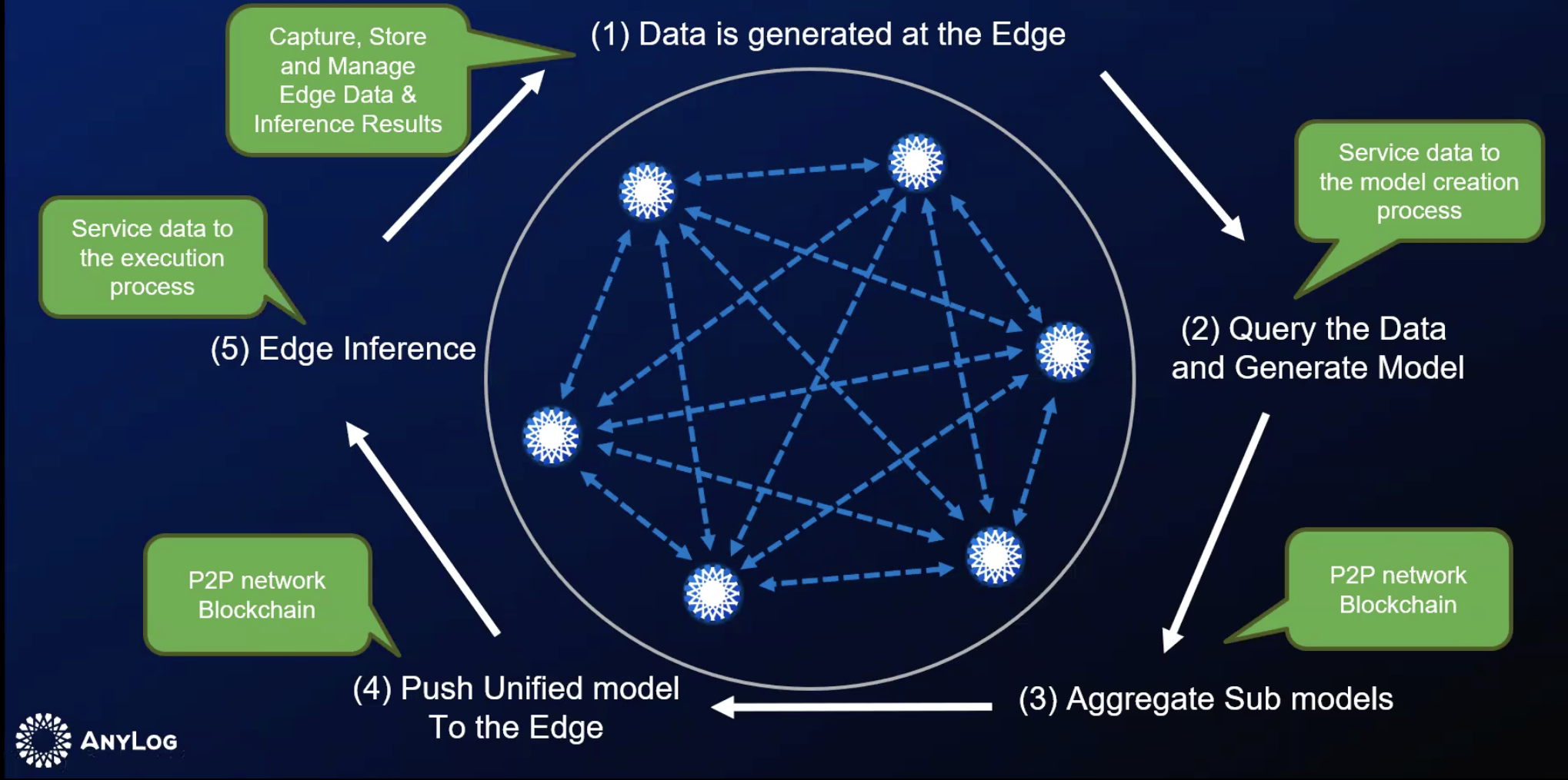
The data at each node is used for local training, creating a ‘sub’ model. The AnyLog software can locate and aggregate all the sub-models to form the complete training model, which is then pushed to each node for AI inferencing at the network edge. The AI learning cycle is repeated – see diagram – to incorporate new data as it is generated.
“All of this is automated,” says Shadmon.
Bypassing the cloud players
Today, the telcos are the leading connectivity providers uploading data from the edge to the cloud.
“But they are not just moving the data; the telcos are also moving the business from the edge to the cloud,” says Shadmon. It is the cloud computing players, not the telcos, that benefit from data hosting and data processing.
However, by virtualizing the data, a telco’s network also serves the end-user’s data requirements; the cloud players are bypassed. Here is an edge opportunity for the telcos. For once, they can take business away from the cloud providers, says Shadmon: “Every per cent of data that remains at the edge and doesn’t go to the cloud is a multi-billion-dollar opportunity for the telcos.”
AnyLog is in discussion with several telcos.

Boosting copper’s reach in the data centre
Marvell has unveiled a chip that enables copper cables to send 1.6 terabits-per-second (Tbps) of data between equipment in the data centre.
Copper cabling, also referred to as direct attach copper, is the standard interconnect used to connect compute nodes in a server, and between servers when building larger computing systems.
Data centre operators prefer to use passive copper cables. A copper cable costs less than an optical cable, a critical consideration when tens of thousands may be used in a large data centre.
Compute servers using the latest processors and AI accelerator chips have increasing input-output (I/O) requirements. This is causing interface speeds between servers, and between servers and switches, to keep doubling—from 400 gigabits to 800 gigabits and soon 1.6Tbps.
Moreoever, with each speed hike, the copper cable’s reach shrinks. A copper cable sending 25 gigabits of data has a reache of 7m, but it is only 2m at 100Gbps and is only 1m at 200Gbps.
The solution is to add a digital signal processing (DSP) chip to the passive copper cabling to create an ’active’ electrical cable. The chip boosts the signal thereby extending the reach. (See diagram below.)

“As speeds go up and the physical distance remains the same, the interconnects have to become active,” says Venu Balasubramanian, vice president of product marketing, connectivity business unit at Marvell.
Marvell says its Alaska chip is the industry’s first to enable 1.6Tbps active electrical cables.
Data centre networking
Two main networks – the front-end and backend – are used in data centres supporting AI workloads.
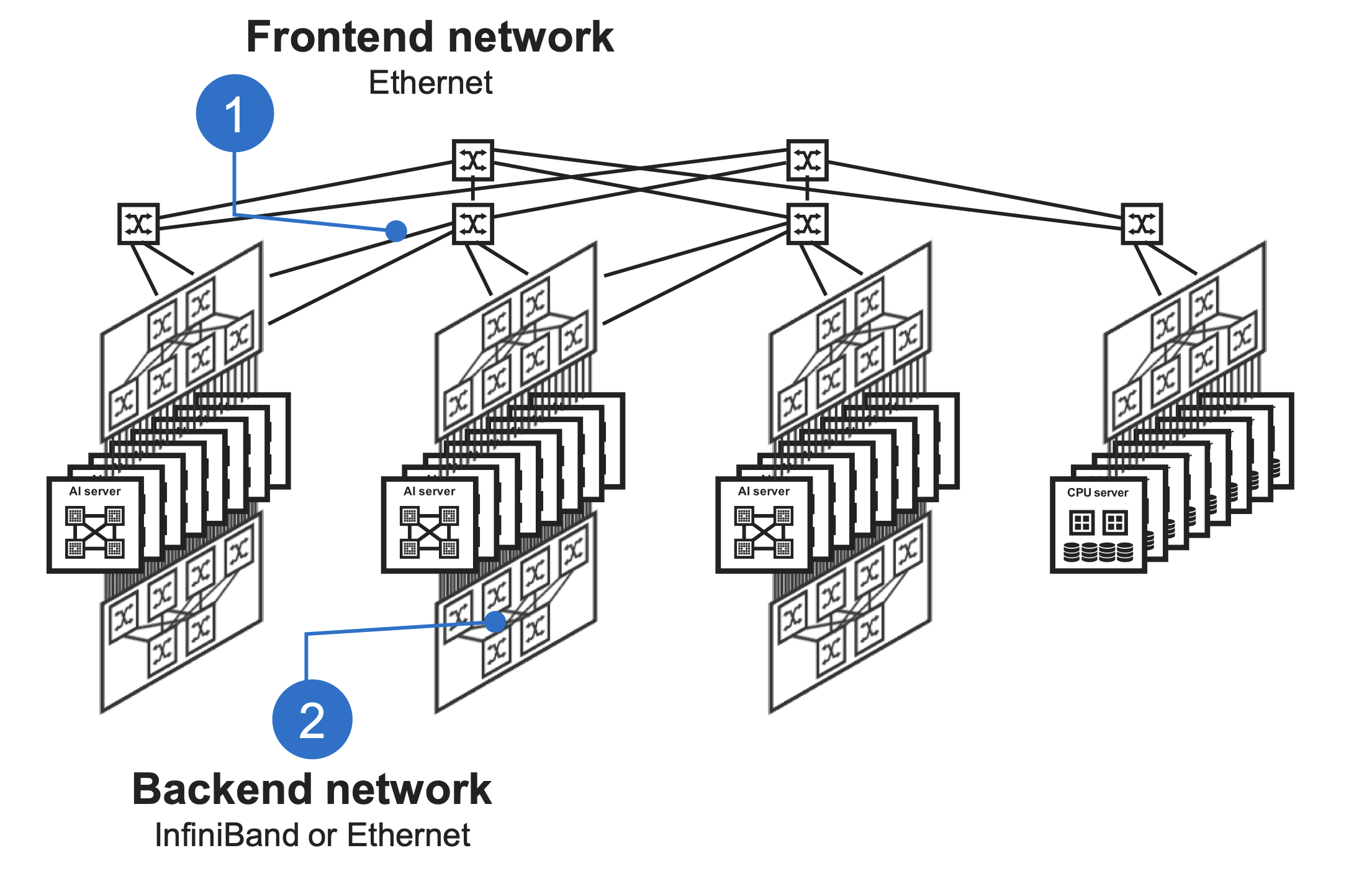
The front-end network, using a traditional Clos network, interfaces servers with the outside world. The Clos network uses a hierarchy of Ethernet switches, with the top-of-rack switches connecting a rack’s servers to leaf and spine switches. The network enables any server to communicate with any other server.
The second, backend network, is optimised to meet the networking requirements of AI. When training an AI model, the servers’ accelerator chips perform intensive calculations before exchanging their results. These steps are repeated many times. The goal is to keep the AI accelerators occupied while ensuring minimal delay when data is exchanged. The backend network’s protocol used to meet these traffic requirements is either Infiniband or Ethernet.
The diagram below shows the typical reaches connecting the compute nodes in a rack and between racks.
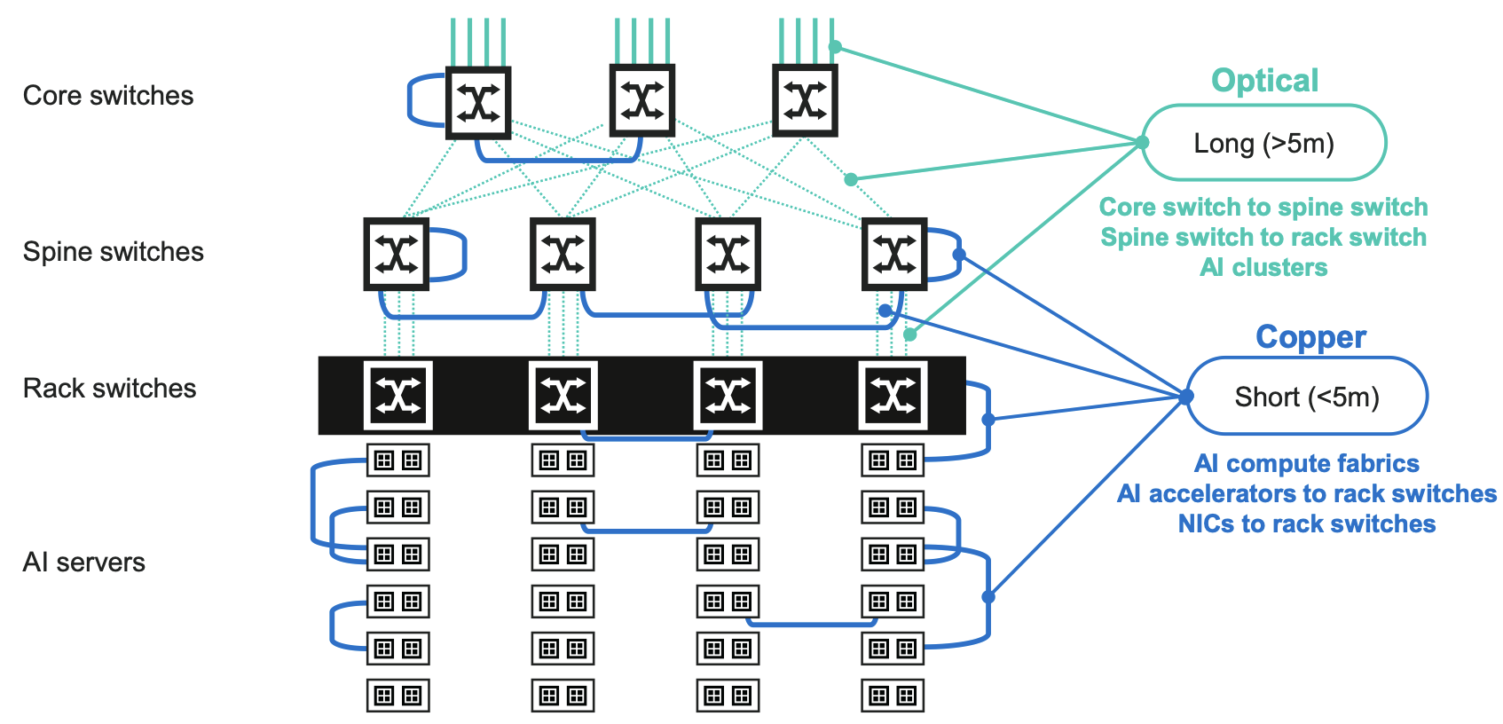
Copper links are preferred for all the links within reach. These are the point-to-point links in a rack and the connections between ervers and the top-of-rack switches. Links between adjacent racks or switches are also within copper’s reach. But optical connections must be used for distances 5m and greater.
“Up to five meters, and previously seven meters, you could connect with passive copper, that has been the interconnect all along,” says Balasubramonian. “Now those links are getting replaced with active copper, and if copper can do it, that is what customers prefer.”
AI accelerator chips’ continual processing performance advancement is also reflected in their I/O requirements.
Nvidia’s latest Blackwell graphics processing unit (GPU) uses 200 gigabit-per-second serialiser-deserialisers (serdes) while AI accelerator designs from other vendor are also adopting 200-gigabit serdes, says Balasubramonian.
The drastic shortening of the reach of passive copper cabling at 200Gbps is driving active electrical cabling usage.
The Alaska DSP
The Alaska chip is implemented using a 5nm CMOS process. To achieve 1.6Tbps, the DSP supports eight channels at 200Gbps, each implementing 4-level pulse amplitude modulation (PAM-4) signalling.
The DSP device amplifies, equalises, and reshapes the signals to achieve extended link distances. The Alaska chip also has a ‘gearbox’ feature that translates between signal speeds. This enables end users to adopt new servers with AI chips that support 200Gbps while using existing switches which may only have 100Gbps ports.
The Alaska chip also includes telemetry and debug features so that data centre operators can note the status of traffic flows and any networking issues.
The chip measures 12mm x14mm, to occupy as little space as possible inside a QSFP-DD or OSFP module, says Balasubramonian.
Using the Alaska device for active electrical cabling means 50Gbps signals can span over 7m, 100Gbps signals over 5m, and 200Gbps signals over 3m.
The 1.6Tbps active electrical cables using the Alaska device also use thinner gauge copper wire. The thinner wiring makes connecting systems easier as the thinner gauge cabling has a higher bend radius. The cabling also improves the air flow, helping equipment cooling.
Marvell says it is working with such active electrical cabling specialists as Amphenol, Molex and TE Connectivity.
Future trends
Marvell points out that AI servers are becoming increasingly distributed. The trend is that a board holding N GPUs will become two boards and in future four boards to host the same number of GPUs.
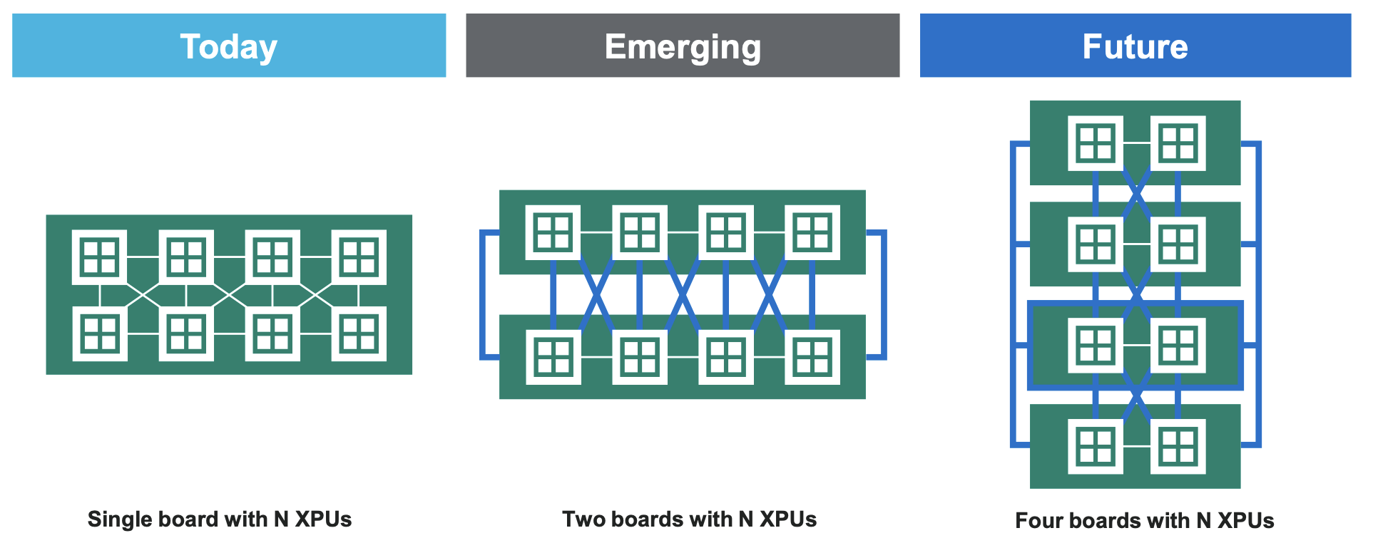
This will requires even more copper interconnects. Passive copper cabling will be used where possible. “If you can do it you with direct attached copper you would do because there will be no power and latency impact [as no DSP chip need be added],” says Balasubramonian.
Marvell expects a combination of passive and active copper cabling to be used in the data centre with the percentage of the links served with passive cabling shrinking as speeds increase.
Marvell typically develops two generations of chip at each speed, with the second released some two years after the first.
The next chip will likely support 1.6Tbps with half the number of channels. This implies 200-gigabit serdes and PAM-4 to achieve 4x400Gbps links.
The cabling will require not just a new generation of serdes but also connectors and cables for a 1.6Tbs active electrical cable implemented using 4x400Gbps channels.
The goal at 400Gbps would be to achieve a reach of 2m. “We don’t yet know [if that is possible],” says Balasubramonian. “It is early.”

Is network traffic growth dwindling to a trickle?
“Network capacities are sufficient, and with data usage expected to plateau in the coming years, further capacity expansion is not needed. We have reached the end of history for communications.”
– Willian Webb, The End of Telecoms History
William Webb has pedigree when it comes to foreseeing telecoms trends.
Webb wrote The 5G Myth in 2016, warning that 5G would be a flop.
In the book, he argued that the wireless standard’s features would create limited interest and fail to grow revenues for mobile operators.

The next seven years saw the telcos promoting 5G and its capabilities. Now, they admit their considerable investments in 5G have delivered underwhelming returns.
His latest book, The End of Telecoms History, argues that telecoms has reached a maturity that satisfies the link speeds needed and that traffic growth is slowing.
“There will be no end of new applications,” says Webb. “But they won’t result in material growth in data requirements or in data speeds.”
What then remains for the telcos is filling in the gaps to provide connectivity everywhere.
Traffic growth slowdown
Earlier this year, AT&T’s CEO, John Stankey, mentioned that its traffic had grown 30 per cent year over year, the third consecutive year of such growth for the telco. The 30 per cent annual figure is the typical traffic growth rate that has been reported for years.
“My take is that we are at about 20 per cent a year annual growth rate worldwide, and it’s falling consistently by about 5 per cent a year,” says Webb.
In 2022, yearly traffic growth was 30 per cent; last year, it was 25 per cent. These are the average growth rates, notes Webb, and there are enormous differences worldwide.
“I was just looking at some data and Greece grew 45 per cent whereas Bahrain declined 10 per cent,” says Webb. “Clearly, there will be big differences between operators.”
He also cites mobile data growth numbers from systems vendor Ericsson. In North America, the growth between 2022 and 2024 was 24 per cent, 17 per cent, and 26 per cent.
“So it is fluctuating around the 20 per cent mark,” says Webb.
Other developments
What about trends like the ever-greater use of digital technologies experienced by many industries, including telecoms? Or the advent of artificial intelligence (AI), which is leading to significant data centre builds, and how AI is expected to change traffic?
“If you look at all non-personal data use, such as the Internet of Things and so on, traffic levels are tiny,” says Webb. There are exceptions, such as security cameras generating video streams. “I don’t see that trend materially changing overall data rates,” says Webb.
He also doesn’t see AI meaningfully growing overall traffic. AI is useful for improving the running of networks but not changing the amount of wireless traffic. “If anything, it might reduce it because you can be more intelligent about what you need to send,” he says.
While Webb admits that AI data centre builds will require extra fixed networking capacity, as will sharing workloads over distributed data centres in a metropolitan area, he argues that this represents a tiny part of the overall network.
He does not see any new devices emerging that will replace the smartphone, dramatically changing how we consume and interact with data.
5G and 6G
Webb also has doubts about the emerging 6G wireless standard. The academic community is busy developing new capabilities for the next wireless standard. “The problem with that is that academics are generally not grounded in the reality of what will make money in the future,” says Webb. Instead, developers should challenge academics to develop the technologies needed for their applications to succeed.
Webbs sees two 6G camps emerging. The first camp wants 6G to address all the shortfalls of 5G using terahertz frequencies and delivering hundreds of gigabits speeds.
“Let’s max out on everything, and then surely, something wonderful must happen,” says Webb. “This strikes me as not learning the lessons of 5G.”
The second camp, including several telcos, does not want to spend any money on 6G but instead wants the technology, in the form of software updates, to address high operational costs and the difficulties in running different network types.
“In this case, 6G improves the operator’s economics rather than improve the end-user offering, which I think makes sense,” says Webb.
“We may end up in a situation where 6G has all this wondrous stuff, and the operators turn around and say they are not interested,” says Webb. “I see a significant risk for 6G, that it just isn’t ever really deployed anywhere.”
Webb’s career in telecoms spans 35 years. His PhD addressed modulation schemes for radio communications. He spent seven years at the UK regulator Ofcom addressing radio spectrum strategy, and he has also been President of the IET, the UK’s equivalent of the IEEE. Webb also co-founded an IoT startup that Huawei bought. For the last 15 years, he has been a consultant covering telecom strategy and technology.
Outlook
The dwindling growth in traffic will impact the telecom industry.
Webb believes the telcos’ revenues will remain the same resulting in somewhat profitable businesses. “They’re making more profit than utilities but less than technology companies,” says Webb.
He also expects there will be more mergers, an obvious reaction to a market flattening out. The aim is to improve profitability.
Given his regulatory background, is that likely? Regulators shun consolidation as they want to keep competition high. He expects it to happen indirectly, with telcos increasingly sharing networks. Each market will offer three or four brands for consumers per market but fewer networks; operators merging in all but name.
Will there even be a need for telecom consultants? “I have to say, as I’ve made these predictions, I’ve been thinking what am I needed for now?” says Webb, laughing.
If he is right, the industry will be going through a period of change.
But if the focus becomes extending connectivity everywhere, there is work to be done in understanding and addressing the regulatory considerations, and also how best to transition the industry.
“I do suspect that just as the rest of the industry is effectively more a utility, it will need fewer and fewer consultants,” he says.

Will AI spur revenue growth for the telcos?
- A global AI survey sponsored by Ciena highlights industry optimism
- The telcos have unique networking assets that can serve users of AI.
- Much is still to play out and telcos have a history of missed opportunities.
The leading communications service providers have been on a decade-long journey to transform their networks and grow their revenues.
To the list of technologies the operators have been embracing can now be added artificial intelligence (AI).
AI is a powerful tool for improving their business efficiency. The technology is also a revenue opportunity and service providers are studying how AI traffic will impact their networks.
“This is the single biggest question that everyone in this industry is struggling with,” says Jürgen Hatheier. “How can the service providers exploit the technology to grow revenues?”
However, some question whether AI will be an telecom opportunity.
“The current hype around AI has very little to do with telcos and is focused on hyperscalers and specifically the intra-data centre traffic driven by AI model training,” says Sterling Perrin, senior principal analyst at HeavyReading. “There is a lot of speculation that, ultimately, this traffic will spread beyond the data centre to data centre interconnect (DCI) applications. But there are too many unknowns right now.”
AI survey
Hatheier is chief technology officer, international at Ciena. He oversees 30 staff, spanning Dublin to New Zealand, that work with the operators to understand their mid- to long-term goals.
Ciena recently undertook a global survey (see note 1, bottom) about AI, similar to one it conducted two years ago that looked at the Metaverse.
Conducting such surveys complements Ciena’s direct research with the service providers. However, there is only so much time a telco’s chief strategy officer (CSO) or chief technology officer (CTO) can spend with a vendor discussing strategy, vision, and industry trends.
“The survey helps confirm what we are hearing from a smaller set,” says Hatheier.
Surveys also uncover industry and regional nuances. Hatheier cites how sometimes it is the tier-two communications service providers are the trailblazers.
Lastly, telcos have their own pace. “It takes time to implement new services and change the underlying network architecture,” says Hatheier. “So it is good to plan.”

Findings
The sectors expected to generate the most AI traffic are financial services (46 per cent of those surveyed), media and entertainment (43 per cent), and manufacturing (38 per cent). Hatheier says these industries have already been using the technology for a while, so AI is not new to them.
Sterling Perrin
For financial services, an everyday use of AI is for security, detecting fraudulent transactions and monitoring video streams to detect anomalous behavior at a site. The amount of traffic AI applications generate can vary greatly. This is common, says Hatheier; it is the use that matters here, not the industry.
“I would not break it down by the industries to say, okay, this industry is going to create more traffic than another,” says Hatheier. “For financial services, if it is transaction data, it’s a few lines of text, but if it is video for branch security, the data volumes are far more significant.”
AI is also set to change the media and entertainment sector, challenging the way content is consumed. Video streaming uses content delivery networks (CDNs) to store the most popular video content close to users. But AI promises to enable more personalised video, tailored for the end-user. Such content will make the traffic more dynamic.
Another example of personalised content is for marketing and advertising. Such personalisation tends to achieve better results, says Hatheier.
AI is also being applied in the manufacturing sector. Examples include automating supply-chain operations, predictive maintenance, and quality assurance.
Car manufacturers check a vehicle for any blemishes at the end of a production line. This usually takes several staff and lasts 10-15 minutes. Now with AI, the inspection can be completed as the cars passes by. “This is a potent application that could run on infrastructure within the manufacturing site but use a service provider’s compute assets and connectivity,” says Hatheier.
The example shows how AI produces productivity gains. However, AI also promises unique abilities that staff cannot match.

Traffic trends
If the history of telecoms is anything to go by, applications that drove traffic in the network rarely lead to revenue growth for the service providers. Hatheier cites streaming video, gaming, and augmented reality as examples.
However, the operators have assets at network edge and the metro that can benefit AI usage. They also have central offices that can act is distributed data centres for the metro and network edge.
Hatheier says users have an advantage if they consume AI applications across a fibre-based broadband network. But certain countries, such as Saudi Arabia and India, mainly use wireless for connectivity.
“AI applications will need to adapt to what is available, and if people want to consume low-latency applications, there is 5G slicing,” says Hatheier. “At the end of the day, there is no way around fibre.”
Optical networking
Government policy regarding AI and regulations to ensure data does not cross borders also play a part.
“It’s an important decision criterion, as we saw in the survey response,” says Hatheier. “So private AI and local computing will be an important decision factor.”
Another critical decision influencing where data centres are built is power. “We see all the gold rush in the Nordics right now with their renewable power and cool climates,” says Hatheier. “You don’t need to cool your servers as much, and it requires a lot of connectivity.”
However, as well as these region-specific data centre builds, there will also be builds in metropolitan areas using smaller distributed data centres.
“Let’s say there are 20 sizable edge or metro compute centres for AI, and you would need three or four to run a big training job,” says Hatheier. “You will not create a permanent end-to-end connection between them because sometimes there will not be four that need to work together, but five, seven, and 11.”
Such a metro network would require reconfigurable optical add-drop multiplexer (ROADM) technology to connect wavelengths between those clusters based on demand to keep sites busy, to avoid expensive AI clusters being idle.
These are opportunities for the CSPs. And while much is still to happen, such discussions are taking place between systems vendors and the telcos.
For Heavy Reading’s Perrin, the more telling opportunity is the telcos’ own use of AI rather than the networking opportunity.
“As a vertical industry, telecom is not typically a leading-edge adopter of any new technology due to many factors, including culture, size, legacy infrastructure and processes, and government regulations,” he says. “I don’t believe AI will be any different.”
Hatheier points to the survey’s finding of general optimism that sees AI as an opportunity rather than a challenge or business risk.
“We have seen very little differences between countries,” says Hatheier. “That may have to do with the fact that emerging countries get as much attention of data centre investment than more developed ones.”

Nokia picks Infinera to boost its optical networking arm
Nokia has announced its intention to buy optical networking specialist Infinera for $2.3 billion.

The motivation for the Infinera acquisition is scale, said Nokia CEO Pekka Lundmark, during an analyst call detailing the announcement.
Optical networking is how communications service providers and hyperscalers cope with the exponential traffic growth.
Continual innovation is required to reduce the cost and power consumed to transport such traffic. For a systems vendor, having scale helps meet these aims.
Optical networking wasn’t always central to Nokia’s strategy. In 2013, Nokia sold its optical networking arm to Marlin Equity Partners, which became Coriant.
Now, Nokia wants to be a leading optical networking vendor by acquiring Infinera, a company that bought Coriant in 2018.
Nokia’s announcement regarding Infinera comes days after it sold its submarine optical networking business. “It’s part of a larger refocusing on core strengths and higher-growth areas,” says John Lively, principal analyst at market research company LightCounting.
Market share and geographical balance
“We estimate that the combined entity will have a 20 per cent market share,” says Jimmy Yu, vice president at market research firm Dell’Oro Group.
Dell’Oro’s vendor ranking data for 2023 gave Huawei a 30 per cent market share, Nokia+Infinera would be second (20 per cent), while Ciena had a 19 per cent share.
Nokia would also strengthen its sales and balance its presence in key markets globally. Infinera has gained webscale customers in recent years, a significant and growing market compared to telecoms.

“Nokia has had competitive long-haul coherent optics in terms of performance but has failed to get much traction outside its traditional CSP markets,” says Lively. “The Infinera deal gives Nokia access to the faster-growing data centre market and a pluggable coherent product line with a strong order pipeline.”
Nokia says the optical networking deal will also strengthen its overall Network Infrastructure business unit that includes IP Networks and Fixed Networks.

Technologies
Nokia and Infinera offer optical networking systems based on high-end embedded coherent modems and coherent pluggable optical modules.
In 2020, Nokia bought Elenion Technologies, giving the company a silicon photonics coherent design team and a way to address the growing pluggable coherent module marketplace.
Early last year, Nokia announced its 1.2-terabit PSE-6s coherent modem for demanding optical transport applications. Two PSE-6s coherent modems can be used to create a 2.4-terabit line card. Nokia started shipping the modem in late 2023 and already has 15 customers.
Infinera is known for its expertise in indium phosphide photonic integrated circuits. The systems vendor’s latest embedded coherent modem is the 1.2-terabit ICE-7 and it offers a range of coherent pluggable products.
Infinera has recently announced design wins for 800-gigabit ZR/ ZR+ for the hyperscale market, and bidirectional 400G ICE-X pluggables for the cable segment. It valued both opportunities at several hundred million dollars, says LightCounting
Dell’Oro’s Yu says Nokia’s acquisition of Infinera would allow it to develop the entire optical front end in-house. He highlights Infinera’s development of indium phosphide, its indium phosphide chip fabrication plants, and the additional optical front-end components such as the trans-impedance amplifier (TIA), driver, and laser.
“The only other vendors with this much done in-house are Huawei and Ciena,” says Yu. “Cisco has all of this except for indium phosphide development.”
Infinera’s success with webscale companies includes optical networking gear for data centre interconnect. The company is also eyeing the optical networking opportunity inside the data centre which promises significant unit volumes. To this aim, the company is developing a range of ICE-D optical engines.
The company has not detailed much about ICE-D besides claiming that it offers power savings of up to 75 per cent. The power-saving claim is based on using a direct-drive approach and a highly integrated design – optics and electronics. Infinera will likely detail first ICE-D offerings at the ECOC show in September.
Once the acquisition is approved, Nokia will have its own lasers and complement its silicon photonics technology with indium phosphide design expertise. Nokia expects to speed up its coherent modem and product roadmap by combining the DSP design teams.
Challenges and Opportunities
Nokia and Infinera are already advanced in the design of their next-generation coherent designs—the PSE-7 and ICE-8, respectively. These are the two companies responses to Ciena’s 200-gigabaud WaveLogic 6 Extreme, which supports up to a 1.6-terabit optical wavelength.
Developing a coherent DSP in a 3nm or 2nm CMOS process is costly. Both companies will continue to develop their designs for now, given that the deal is expected to close in the first half of 2025. However, they will be keen to agree on what design to choose. This had happened before when Infinera halted what would have been the ICE-5 in favour of Coriant’s design and turned its full attention to developing the ICE-6.
The industry is challenged to keep driving down the cost-per-bit and power-per-bit. The preferred approach is to keep increasing the symbol rate even if the spectral efficiency gains are more modest with each generation due to Shannon’s limit being approached.
However, increasing the baud rate is increasingly challenging and will lead to new parallel designs. Pooling the two companies’ coherent design expertise will help here.
Nokia says another factor for the deal is the expected growth in AI traffic. Such AI traffic is on top of fixed and mobile traffic growth. AI will drive intra-data and inter-data centre networking in the core and edge. Such traffic will be for training and inferencing.
The rest
There will be a notable gap between the top 3 and the remaining optical vendors, who all have a single digital market share. However, the consensus is that the niche players will have a role. Since telecom equipment is a critical infrastructure, operators and governments must promote using local vendors when available. Yu cites the examples of the Padtecs in South America and Tejas in India.

Cloud and AI: Opportunities that must be grabbed
The founder of Cloud Light, Dennis Tong, talks about the company, how its sale to Lumentum came about, and the promise of cloud and AI markets for optics.

For Dennis Tong (pictured), Hong Kong is a unique place that has a perfect blend of the East and West.
Tong, the founder and CEO of optical module specialist Cloud Light, should know. The company is headquartered in Hong Kong and has R&D offices in Hong Kong and Taipei, Taiwan. Cloud Light also has manufacturing sites in Asia: in the Chinese city of Dongguan—two hours by car, north of Hong Kong—and in the Philippines.
Now, Cloud Light is part of Lumentum. The U.S. photonics firm bought the optical module maker for $750 million in November 2023.
Tie-up
Cloud Light is a volume manufacturer of optical modules. The company takes 12-inch silicon photonic wafers, tests the wafers’ dies, and packages them for use in optical modules.
Cloud Light has a long relationship with Lumentum, using the U.S. company’s continuous-wave lasers for its silicon photonic-based optical modules.
Tong says he has been in photonics for 30 years and has good friends at Lumentum. “We had opportunities to chat and exchange views as to where the industry is going, and we shared a common vision,” he says. Eventually, the talk turned to a possible merger and acquisition.
Tong says the decision to sell the company centred on how best to grow the company. Cloud Light would have continued to do well, he says, but the company could grow much faster if he and his 1,600 staff joined Lumentum.
It is also timely. “Opportunities such as cloud and AI, they don’t come along very often,” says Tong.

Wafer-in, Product-out
Cloud Light has developed a manufacturing process dubbed “wafer-in, product-out.”
Turning a photonic integrated circuit (PIC) into a packaged optical module involves many stages and players. Designers of a PIC pass it to a foundry that results in the wafer. The wafer is shipped to an outsourced semiconductor assembly and test (OSAT) that does wafer back-end tasks: testing and dicing the wafer, and polishing. The working PICs—the known good dies—are shipped to a contract manufacturer that makes the pluggable modules.
“You can see that the entire collaboration chain is fragmented,” says Tong. “With our wafer-in, product-out process, we put everything in one group.”
Cloud Light takes the wafer from the foundry and does all the steps resulting in the delivered module.
Tong says the advantage of undertaking the complete process includes improved product yield. For example, the company measures coupling loss to the PIC and its optical waveguide loss during testing, and uses the insight to improve product yield.
Cloud Light has developed its own equipment to support automation. This know-how means that its design staff can work with the process and equipment colleagues to tailor the manufacturing process for new product designs. The precise assembly of unique micro-optics is one example.
It is this expertise and capability that particularly interested Lumentum in Cloud Light.
According to Tong, accumulating expertise in the different production areas has taken years: “There is a lot of subtlety to it, and we started to set this up in 2017.”
Hyperscaler business
Cloud Light succeeded early with a hyperscaler, making a 4×10-gigabit multimode VCSEL-based transceiver. But it soon realised market growth was coming from single-mode optical transceivers.
Its decision to pursue its wafer-in, product-out strategy stemmed from a desire to avoid becoming one of many single-mode optical transceiver makers. “We didn’t think we would add any value to the market by just creating a me-too company,” says Tong.
If the company was going to invest in a new platform, it would have to be scalable to support high volumes.
“It was very clear that silicon photonics was the right thing to do,” says Tong. “We were one of the first, if not the first, to launch a 400-gigabit silicon photonics-based transceiver in 2019.”
Cloud Light pitched its in-house scalable manufacturing approach to a hyperscaler that liked its plan, resulting in the company securing the hyperscaler as a customer.
Plans
Since the acquisition’s completion, Lumentum has given Cloud Light broad scope; there is no rush for full-blown integration, says Tong.
“Our mandate is to continue to grow the module business,” he says. “And we are open to using components from Lumentum and other suppliers.”
Lumentum’s components also offer Cloud Light the ability to create new products. “Customers are seeing us as more equipped, which opens up new, interesting opportunities,” says Tong.
Moreover, Cloud Light is not solely making modules for Lumentum. “The reality is that this is a very dynamic market, dominated by a few customers,” says Tong. “We are open to different business models as long as we can add value.”
Opportunities
At the time of the deal, Lumentum revealed that it expected Cloud Light would add $200 million plus to its yearly income. Cloud Light’s $200 million in revenues in the previous year was almost all from 400-gigabit and higher-speed transceiver sales.
Lumentum also makes coherent optical modems, ROADMs, and 3D sensing for commercial applications. Tong says coherent modules are one obvious opportunity for Cloud Light: “If you look into the future, I think the line between cloud/ datacom and telecom will become blurred.”
Cloud and AI will drive volumes, and the silicon photonics platform will be applicable for coherent modems as well. “So, a lot of the things that we have developed will also be applicable to coherent modules in the future,” says Tong. “And it is definitely applicable if one day coherent optics makes its way into the data centre.”
Coherent optics modules will keep increasing symbol rate and use more sophisticated coding schemes, but at some point, the effective data rate per line will start to plateau. To increase bandwidth beyond that, designs will go parallel by adding more channels. “Adding more fibre or more wavelengths, then it comes back to density, and then it’s all about packaging,” says Tong.
The ability to change its automated assembly for new applications also suggests that Cloud Light’s manufacturing capability could benefit Lumentum’s other product lines, such as ROADMs and even new markets such as optical circuit switches.
Co-packaged optics
Co-packaged optics are seen as one solution for applications where standard pluggable optics are no longer suitable.
Tong says that there are still issues before co-packaged optics are deployed at scale. One challenge is reliability; hyperscalars will not deploy the technology at scale until it has demonstrable good quality and reliability.
“The emergence of AI and cloud may accelerate that deployment, simply because of the volumes they are using and the density issue,” says Tong. Cost and thermal issues is also something co-packaged optics can address.
Cloud Light is ready for the advent of co-packaged optics. For its 800-gigabit transceiver, it can package a bare-die digital signal processor right next to the silicon photonics optical engine. “It’s not exactly a co-packaged optics product, but it has the same capability,” he says.
Shrinking lifecycles
The lifecycle of optical module products continues to shrink. At 10 gigabits, it was a decade-plus; for 100 gigabits, it was five to six years; at 400 gigabits, it has been more like three or four years. “Now, with AI, it is more like two to three years,” says Tong.
To be successful, it is all about time-to-market and time-to-scale.
“You need to be able to ramp up very quickly to the type of volumes and the type of quality that the customer is asking for,” says Tong. “There’s no time for you to get ready; you must be ready.”

DustPhotonics raises funding for 800G and 1.6T modules
- DustPhotonics has raised $24 million in funding.
- The start-up has taped out its 200 gigabit-per-lane optical chip.
- DustPhotonics expects the 1.6-terabit module market to ramp, starting year-end.
DustPhotonics, which develops chips for transmit optical sub-assemblies (TOSAs) for 400 and 800-gigabit pluggable optical modules, has raised $24 million. The funding extends its Series B funding round.
“When you start ramping up products, you have to iron out the creases around supply chain, production, and everything else,” says Ronnen Lovinger, CEO of DustPhotonics.
DustPhotonics has several customers and a backlog of orders for its 400 and 800-gigabit photonic integrated circuits (PICs). The company has also taped out its 200 gigabit-per-lane chip and will have products later this year.
800-gigabit PICs
DustPhotonic’s products include the Carmel-4-DR4, a 400-gigabit DR4 PIC, and several variants of its 800-gigabit Carmel-8.
“Most of our customers and engagements are interested in the 800-gigabit applications,” says Lovinger.
DustPhotonics has developed a way of attaching a laser source to its silicon photonics chip with sub-micron accuracy. The company uses standard off-the-shelf continuous-wave lasers operating at 1310nm.
The efficiency of the laser-attach scheme means one laser can power four channels, or two lasers can be used for a DR8 design, reducing cost and power consumption.
At the ECOC show last October, DustPhotonics unveiled three 800-gigabit Carmel-8 products. The products include a DR8 with a reach of 500m, a 2km DR8+, and an 800-gigabit ‘lite’ version that competes with 100-gigabit VCSEL designs and only uses one laser. Several customers are considering the Carmel-8-Lite for Ethernet and PCI Express applications.
Manufacturing
DustPhotonics is working with foundry Tower Semiconductors as it goes to production.
“Having a strong fab partner is very important for silicon photonics,” says Lovinger, who views Tower as a leading silicon photonics foundry. “We have been working with Tower for five years, and they have been a strong partner.” DustPhotonics is using several partners for device assembly.
DustPhotonics is headquartered in Israel and has 50 staff, 37 of whom are in R&D. Investors in the latest funding round include Sienna Venture Capital, Greenfield Partners, Atreides Management, and Exor Ventures.
Lovinger will attend the OFC show later this month for meetings with customers and prospects. “It is always good to see so many customers under the same roof,” he says.
200-gigabit optical
DustPhotonics has a highly stable silicon-photonics modulator that does not need to be temperature-controlled and operates at 200 gigabits per lane.
Developing a 200 gigabit-per-lane transmit chip means that DustPhotonics can address a 4-lane 800-gigabit DR4 and an 8-lane 1.6-terabit DR8 modules.
Lovinger says that many driver and digital signal processing chip companies already offer 800 gigabit/ 1.6-terabit chips. Thus, he sees the advent of 1.6 terabit modules as straightforward once its TOSA design is ready.
“Once we have 200 gigabits-per-lane, it takes us to 1.6 terabits and, in some configurations, 3.2 terabits,” says Lovinger. “We see the 1.6-terabit market starting at the end of this year and ramping in 2025.”
Lovinger says the progress of pluggable modules is postponing the need for co-packaged optics. That said, the company says it has the technologies needed to address co-packaged optics when the market finally needs it.

imec's novel ADC promises faster sampling rates
The analogue-to-digital and digital-to-analogue converters (ADCs/DACs) are like the equals sign in mathematics.
The equals sign is taught as showing two sides of an equation being the same. But really, it is a gateway between two worlds. The same applies to the ADC and DAC, which equate between the analogue and digital worlds.
Progress in wireline communications, whether client-side optics or coherent optical modems at 800 gigabits and soon 1.6 terabits, means converters must sample at higher rates.
In February, at the IEEE International Solid-State Circuits Conference (ISSCC) in San Francisco, imec detailed a proof-of-concept chip design that promises to advance high-speed ADCs.
In the paper, the authors from the Belgium nano and digital technology innovation centre detailed a 16nm CMOS 7-bit ADC test chip operating at 42 Giga-samples per second (GSps). The speed is not particularly noteworthy, but the design is: a tiny ADC circuit that promises future faster designs.
imec believes a 250-300GSps ADC will be possible when implemented in a state-of-the-art 2nm or 3nm CMOS process.
Converters for comms
I am text block. Click edit button to change this text. Lorem ipsum dolor sit amet, consectetur adipiscing elit. Ut elit tellus, luctus nec ullamcorper mattis, pulvinar dapibus leo.
Time-interleaved SAR
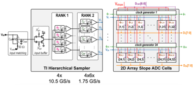
For such high-speed ADCs, a time-interleaved successive approximation register (SAR) architecture is commonly used. The converter design is relatively small and power efficient. Van Driessche says imec has almost two decades of experience designing such ADCs.
The time-interleaved refers to the sampled high-speed signal being distributed across parallel ADC channels. Van Driessche cites as an example a 100GSps ADC that distributes the samples to 100 such interleaved channels, each operating at 1GSps.
“The input [to the ADC] is still operating at full speed, but your ADCs, or channels, operate at a hundredth of the speed,” says Van Driessche.
The issue with a time-interleaved SAR-based converter is that as the speed increases, so does size. The result is longer interconnect lines linking the channels and distributing the clocking signal.
“Distributing the signal and the clock over long lines leads to large parasitics,” says Van Driessche. And with parasitics comes a higher power consumption and/or a lower overall analogue bandwidth.
imec’s ISSCC ADC (see diagram) simplifies the SAR circuitry. Dubbed a time-interleaved slope ADC, each channel is even slower than the traditional design. But the primary circuit is tiny, comprising a sampling switch, sampling capacitor, comparator, and a few digital gates. Reducing its size and arranging multiple such units in a 2D array shortens the interconnects, lowering the power and widening the circuit’s bandwidth.
The result is a compact design and a much-reduced power consumption. “This is the essence: to make the core of the ADC significantly smaller, smaller than any alternative that we are aware of,” says Van Driessche.
5nm CMOS design
The ISSCC paper reports the results of a 16nm test chip operating at 42GSps. “You first need to prove that it works,” says Van Driessche. The core’s area is 0.07mm2 only.
Now, imec is working on a 5nm CMOS version. The smaller and faster transistors help achieve higher sampling rates and better power efficiency. But it also comes with challenges: much more impact from parasitics limiting the analogue bandwidth and the resulting speed, and obtaining sufficient output voltage swing at low-power consumption for the DAC.
“The real benefit of the novel ADC architecture comes when you go to higher sampling rates,” says Van Driessche. imec is not saying how fast, but it expects it to exceed 150GSps significantly. Imec expects to tape out the ADC alongside an equivalent DAC next month, with measurement results expected by year-end.
Based on simulation results, imec expects to halve the ADC’s power consumption compared to other similar-speed ADCs. Designers get a notable power saving or can use two channels for the same power.
At OFC 2023, Imec detailed how it expects to achieve sampling rates of 250GSps for a 3nm CMOS coherent DSP design.
How much faster can ADCs go?
Van Driessche says that in future, the gains from technology scaling will diminish, requiring very skilled designers and a huge amount of effort.
“At some point, and I cannot say when, there will be diminishing returns,” he says. “We are not there yet, but we are getting closer.”
Once companies decide that a limit is reached, several parallel channels will be needed, a development designers will want to avoid for as long as possible.

OFC 2024 reflects a mature industry with new offshoots
- The three General Chairs preview the upcoming Optical Fiber Communications (OFC) conference and discuss photonics developments and trends.
- The General Chairs' role is to choose the plenary speakers, programme theme, and conference schedule.
- OFC takes place during March 24th-28th in San Diego, CA.*
Photonics, at least for traditional applications, has become a mature industry. So says Professor Dimitra Simeonidou, one of this year’s OFC General Chairs.
y traditional, Simeonidou is referring to classical optical communications.
But she also stresses new developments: the use of optical fibres for environmental sensing, optics for satellites, and quantum.
“Quantum is like a micro-OFC,” says Simeonidou. “You have issues from technology to subsystem to system applications now appearing in the OFC programmes.”