
Silicon photonics grapples with 3D packaging demands
Hesham Taha (pictured), CEO of start-up Teramount, is more upbeat about silicon photonics than ever. But, as he outlines, challenges remain.
Hesham Taha is putting in the miles. The CEO of Teramount has been travelling to the East and West to meet with companies.
Termount is working closely with customers and partners adopting its technology that adds fibre to silicon photonics chips.
“We’re shipping units to customers and partners, and we need to be close to them as they integrate our components and address the challenges of integration,” says Taha.
Teramount
For Taha, connecting fibre to a silicon photonics chip inside a pluggable optical transceiver is relatively straightforward.
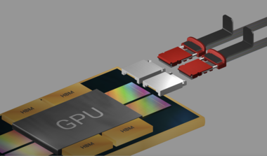
Far more challenging is when the optical engine and chip are packaged together, known as co-packaged optics. Such a tight coupling raises reliability challenges.
The optical engine is close to the large, heat-generating chip, introducing manufacturing and reliability issues. Also, the fibre-connect to the optical engine inside the package must be scalable. Scaling is key because with each chip generation – whether an AI accelerator or a switch chip – the input-output (I/O) requirements grow.
Teramount’s technology couples the fibre to the silicon photonics chip using a photonic plug and photonic bump.
The photonic plug holds the fibres and couples them to the silicon photonics chip via a photonic bump, a component made during the silicon photonics wafer’s processing.
The photonic bump has two elements: a wideband deflector and a lens mirror for beam expansion. Expanding the light beam enables larger assembly tolerances.
The resulting wafer-level manufacturing may be more complicated, says Taha, but the benefits include relaxed tolerances in the assembly, wideband surface coupling, and the testing of the wafer and the die.
The photonic bump-and-plug combination also enables detachable optics for co-packaged optics designs, benefitting their manufacturing. (For more about Teramount’s technology, click here)
Silicon Photonics meets semiconductor thinking
Taha sees silicon photonics as a platform that enables the integration of optical functions at the wafer scale using standard semiconductor manufacturing techniques.
“It [silicon photonics design] has the same way of thinking as semiconductor people: chip designers, foundries, and packaging people,” says Taha. The result is that silicon photonics is bringing optics to chip design.
The growing maturity of the technology, and the emergence of foundries such as TSMC, GlobalFoundries, Tower Semiconductor, Intel, and ST Microelectronics offering silicon photonics, means that companies with photonic designs can be fabless; a model that has benefitted the chip industry.
Photonic chip designers can use a large foundry’s process design kit (PDK) and send off their silicon photonics designs to be manufactured in volume.
As for co-packaged optics, Taha sees it as a key in the evolution of silicon photonics. Co-package optics is the realisation of silicon photonics whereby optics is integrated next to advanced semiconductor chips.
Industry developments
The growing interest in silicon photonic and co-packaged optics is also evident in some recent announcements, driven by the AI compute scaling needs.
ST Microelectronics unveiled its 300mm wafer PIC100 silicon photonics technology. ST Microelectronics was active in silicon photonics 10 years ago and has returned due to the AI opportunity.
Marvell announced it offers a co-packaged optics solution for accelerator chips to address scale-up networking for AI architectures.
Leading foundry TSMC has outlined its silicon photonics roadmap, which includes co-packaged optics.
And at the GTC 2025 AI developers conference, Nvidia announced it is adding co-packaged optics to its switch platforms for scale-out networking.
“All this is not a surprise because this is where we expected silicon photonics to be one day when we founded the company 10 years ago,” says Taha. “It is just that this day is happening now.”
Teramount sees its fibre attach product as a part of an emerging ecosystem to enable standard semiconductor high-volume manufacturing.
This ecosystem comprises chip designers, foundries, OSATs [outsourced semiconductor assembly and test service providers], and system integrators.
But there are challenges. There may be wafer-scale manufacturing, but issues remain on the integration-packaging side.
“This is why we need to travel, to align with the different partners,” says Taha.
Challenges
Teramount is seeing challenges first-hand given its fibre-attach vantage point. Taha also highlights commercial issues still to be resolved.
The technical challenges revolve around integrating the silicon photonics die with the accompanying lasers and fibres in an advanced package.
Unlike a traditional pluggable optical transceiver, the silicon photonics chip is inserted in a hot environment and must meet operational temperatures of 85oC and even 105oC.
Multiple reflow soldering steps during manufacturing expose the packaging to even higher temperatures (270oC) and thermal stresses.
“These are new technical challenges that silicon photonic chip integration must meet 3D packaging requirements,” says Taha.
3D packaging has requirements that affect the fibre attach. For example, the silicon photonics chip is thinner than the die used in a pluggable if through-silicon via (TSV) technology is used.
TSV refers to the way a vertical electrical connector is done that passes through the die. Any mechanical stresses or warpage impacts the resulting optical performance of the die.
“Co-package optics is creating new challenges when connecting fibre to such thinner chips,” says Taha.
There are also issues with testing a design. “There are still no mature solutions for parallel optical and electrical testing,” says Taha.
The commercial issue he highlights centres around design ownership. With a pluggable module, all the components are delivered in one assembled device with one owner – the module maker.
With co-packaged optics, there are several stages of assembly, with components coming from multiple sources. “Who owns it?” says Taha.
Box system integrators making servers, switches, and the like don’t work with fibre. In contrast, co-packaged optics require connecting and managing hundreds of fibres that fit in a tight space. Good optical coupling and performance are a must to ensure the overall design.
“So this flow [for co-package optics] has yet to be set,” says Taha.
He says all the players, chip designers, foundry packaging vendors (OSATs), and system integrators still need to be aligned. That said, the industry, particularly the large silicon chip vendors, are working to make it happen, says Taha.
This implies that companies such as Nvidia, Intel, AMD, Broadcom, and Marvell are playing a key role here.
Given how the emerging AI opportunity is driving their chip businesses, they have every reason to make this work.

Adtran broadens its OLS and access module offerings
Adtran has unveiled two products before the OFC show in San Francisco taking place at the end of the month.
One is a 50 gigabit-per second (Gbps) SFP56 optical transceiver that uses 4-level pulse-amplitude modulation (PAM-4) for 5G front-haul and enhanced broadband applications.
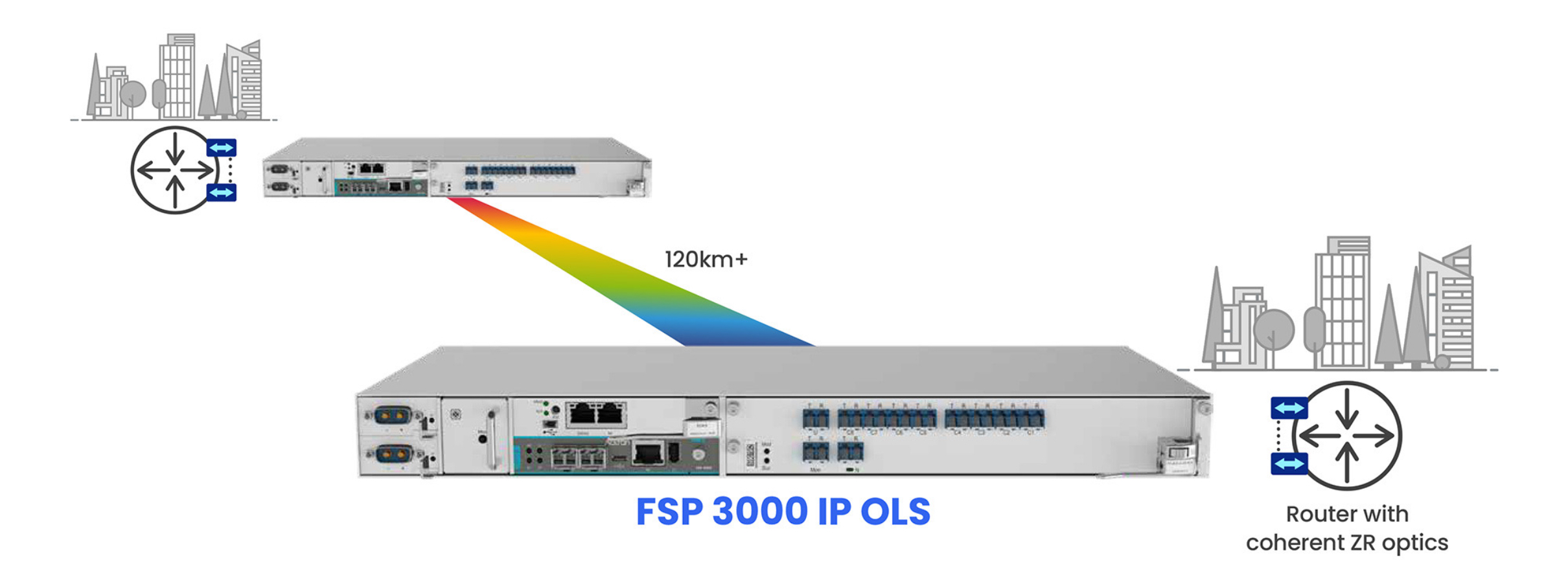
The second product is the FSP 3000 IP OLS, a compact open line system (OLS) designed for point-to-point links between sites 120km apart.
The OLS has been developed to simplify the setting up of dense wavelength division multiplexing (DWDM) optical links.
Enhancing broadband
Adtran has been developing a range of transceiver products to address specific requirements in the access-aggregation marketplace.
These include the MicroMux Edge Bidi, a QSFP+ pluggable module that supports 4×10 gigabit signals over 40km for mobile backhaul and enterprise wireless applications.
Adtran also offers the AccessWave25, a 25-gigabit tunable wavelength transceiver in an SFP28 form factor with a reach of 40km.
The pluggable module is used to link remote physical layer devices (RPDs) in cable operators’ networks. Cable operators are upgrading their infrastructure from 10 gigabits to 25 gigabits to support DOCSIS 4.0.
“You can argue if DOCSIS 4.0 is here or coming at the year-end,” says Saeid Aramideh, vice president of business development, optical engines business unit, at Adtran. “But there is no argument about the need for 25-gigabit uplinks for the cable MSO market.”
Now Adtran is announcing the AccessWave50, a 50-gigabit SFP56 optical module for fronthaul, part of the radio access network (RAN) and for other developments driving traffic such as smart homes, Internet of Things, and Smart Cities.
Aramideh refers to these applications as driving ‘enhanced’ broadband networks, requiring the upgrading of 25 gigabit links to 50- and even 100-gigabit ones.
Front-haul networks
For mobile, telco operators and RAN equipment makers are working with optical component makers to drive innovation in pluggables for emerging architectures such as enhanced 5G and 6G, says Aramideh.
In mobile networks, the front-haul network carries radio signals using the CPRI (common public radio interface) or enhanced CPRI protocols between the remote radio heads and the baseband units.
For 5G front-haul, the modules used are mainly at 10 gigabits-per-second (Gbps) with some 25-gigabit modules deployed. Adtran’s AccessWave50 addresses the next speed hike.
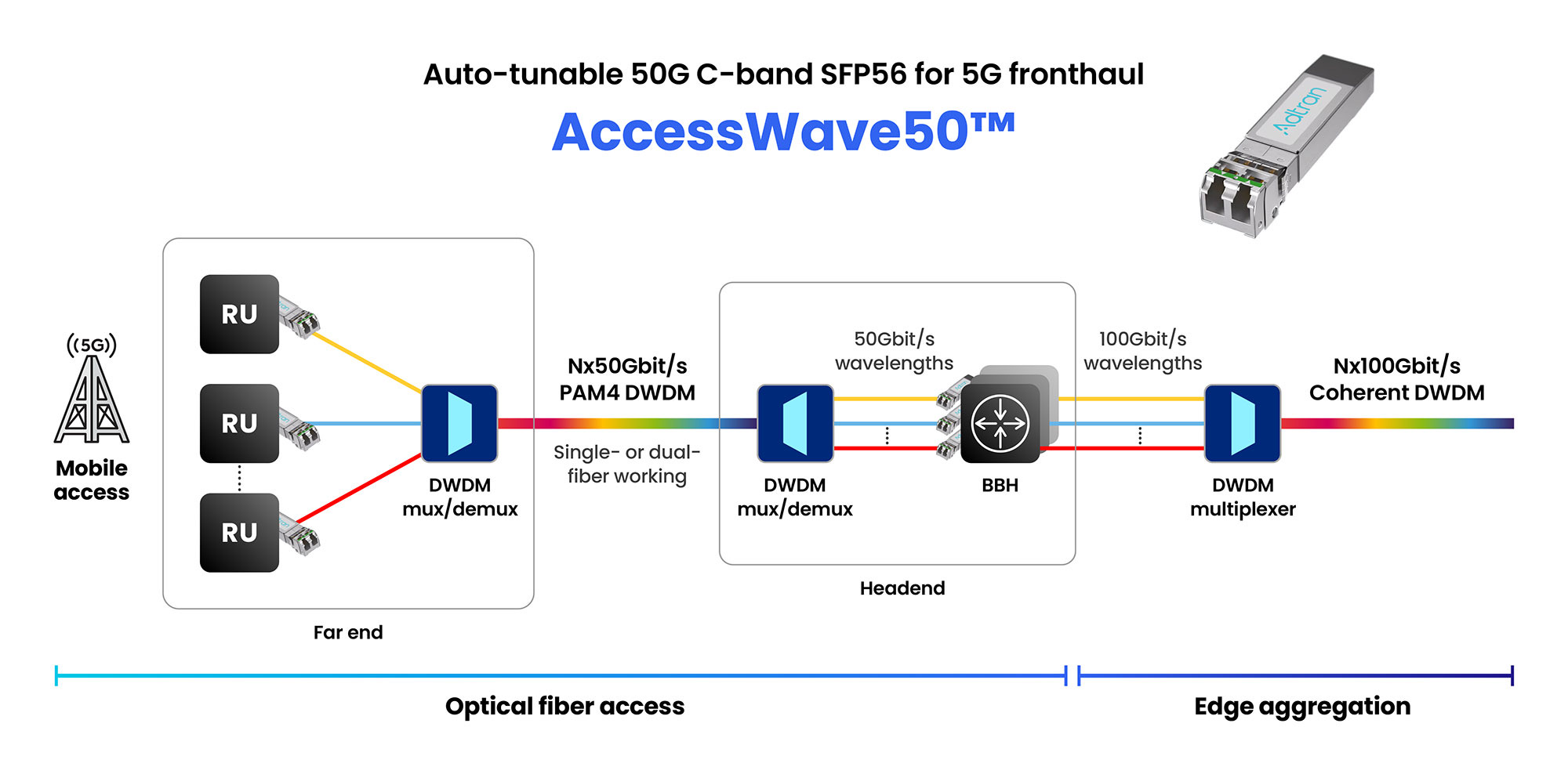
Adtran has designed the AccessWave50 using proprietary signal-shaping and distance optimisation techniques along with 4-level pulse amplitude modulation (PAM-4) to achieve the 50Gbps line rate.
“PAM-4 is proving itself to be a cost-performance-optimised technology and give you spectral efficiency as you go to higher data rates,” says Aramideh. “Of course, it’s not coherent optics, but you don’t need coherent for all applications.”
AccessWave50 uses a tunable laser and has a 15km, not 40km reach, but that is sufficient, says Aramideh, since front-haul networks are latency-constrained. The SFP56 module consumes 2.5W only.
Compact networking
Adtran has also unveiled its latest open line system (OLS) for C-band coherent transceivers.
The company has been providing bespoke OLS systems for hyperscalers. ADVA, the company Adtran acquired in 2022, provided Microsoft with the OLS that, working with the original ColorZ modules from Marvell, enabled 100 gigabit PAM-4 transmissions over 80km links.
Adtran also provides an OLS for data centre interconnects using 400ZR coherent modules for reaches of 120km.
The latest FSP 3000 IP OLS platform is a compact one-rack (1RU) high box that supports eight wavelengths over 120km.
The platform also includes an OTDR (optical time domain reflectometer) for fibre diagnostics.
The OLS can be used with 400-gigabit, 800-gigabit, and ultimately 1.6 terabit coherent pluggable modules once available.
The OLS is also designed for telecom metro interconnect networks. “Telcos, in response to AI, are also looking for OLS technology tailored to coherent transceivers,” says Stephan Rettenberger, senior vice president of marketing and corporate communications at Adtran.
A chief design challenge has been to fit the OLS into a 1 RU form factor, requiring integration and packaging work. The OLS has also been designed to be set up and operated straightforwardly.
The platform is scalable: two racks stacked double the wavelength counts to 16.
The FSP 3000 IP OLS product is already in the hands of one telco customer, says Rettenberger.

Broadcom’s silicon for the PCI Express 6.0 era
Broadcom has detailed its first silicon for the sixth generation of the PCI Express (PCIe 6.0) bus, developed with AI servers in mind.
The two types of PCIe 6.0 devices are a switch chip and a retimer.
Broadcom, working with Teledyne LeCroy, is also making available an interoperability development platform to aid engineers adopting the PCIe 6.0 standard as part of their systems.
Compute servers for AI are placing new demands on the PCIe bus. The standard no longer about connects CPUs to peripherals but also serving the communication needs of AI accelerator chips.
“AI servers have become a lot more complicated, and connectivity is now very important,” says Sreenivas Bagalkote, Broadcom’s product line manager for the data center solutions group.
Bagalkote describes Broadcom’s PCIe 6.0 switches as a ‘fabric’ rather than silicon to switch between PCIe lanes.
PCI Express
PCIe is an long-standing standard adopted widely, not only for computing and servers but across industries such as medical imaging, automotive, and storage.
The first three generations of PCIe evolved around the CPU. There followed a big wait for the PCIe 4.0, but since then, a new PCI generation has appeared every two years, each time doubling the data transfer rate.
Now, PCIe 6.0 silicon is coming to the market while work continues to progress on the latest PCIe 7.0, with the final draft ready for member review.
The PCIe standard supports various lane configurations from two to 32 lanes. For servers, 8-lane and 16-lane configurations are common.
“Of all the transitions in PCIe technology, generation 6.0 is the most important and most complicated,” says Bagalkote.
PCIe 6.0 introduces several new features. Like previous generations, it doubles the lane rate: PCIe 5.0 supports 32 giga-transfers a second (GT/s) while PCIe 6.0 supports 64GT/s.
The 64GT/s line rate requires the use of 4-level pulse amplitude modulation (PAM-4) for the first time; all previous PCIe generations use non-return-to-zero (NRZ) signalling.
Since PCIe must be backwards compatible, the PCIe 6.0 switch supports PAM-4 and NRZ signalling. More sophisticated circuitry is thus required at each end of the link as well as a forward error correction scheme, also a first for the PCIe 6.0 implementation.
Another new feature is flow control unit (FLIT) encoding, a network packet scheme designed to simplify data transfers.
PCIe 6.0 also adds integrity and data encryption (IDE) to secure the data on the PCIe links.
AI servers
A typical AI server includes CPUs, 8 or 16 interconnect GPUs (AI accelerators), network interface cards (NICs) to connect to GPUs making up the cluster, and to storage elements.
A typical server connectivity tray will likely have four switch chips, one for each pair of GPUs, says Bagalkote. Each GPU has a dedicated NIC, typically with a 400 gigabit per second (Gbps) interface. The PCIe switch chips also connect the CPUs and NVMe storage.
Broadcom’s existing generation PCIe 5.0 switch ICs have been used in over 400 AI server designs, estimated by the company at 80 to 90 per cent of all deployed AI servers.
Switch and retimer chips
PCIe 6.0’s doubling the lane data rate makes sending signals over 15-inch rack servers harder.
Broadcom says its switch chip uses serialiser-deserialiser (serdes) that outperform the PCIe specification by 4 decibels (dB). If an extra link distance is needed, Broadcom also offers its PCIe 6.0 retimer chips that also offer an extra 4dB.
Using Broadcom’s ICs at both ends results in a 40dB link budget, whereas the specification only calls for 32dB. “This [extra link budget] allows designers to either achieve a longer reach or use cheaper PCB materials,” says Bagalkote.
The PCIe switch chip also features added telemetry and diagnostic features. Given the cost of GPUs, such features help data centre operators identify and remedy issues they have, to avoid taking the server offline
“PCIe has become an important tool for diagnosing in real-time, remotely, and with less human intervention, all the issues that happen in AI servers,” says Bagalkote.
Early PCIe switches were used in a tree-like arrangement with one input – the root complex – connected via the switch to multiple end-points. Now, with AI servers, many devices connect to each other. Broadcom’s largest device – the PEX90144 – can switches between its 144 PCIe 6.0 lanes while supporting 2-, 4-, 8- or 16-lane-wide ports.
Broadcom also has announced other switch IC configurations with 104- and 88-lanes. These will be followed by 64 and 32 lane versions. All the switch chips are implemented using a 5nm CMOS process.
Broadcom is shipping “significant numbers” of samples of the chips to certain system developers.
PCIe versus proprietary interconnects
Nvidia and AMD that develop CPUs and AI accelerators have developed their own proprietary scale-up architectures. Nvidia has NVLink, while AMD has developed the Infinity Fabric interconnect technology.
Such proprietary interconnect schemes are used in preference to PCIe to connect GPUs, and CPUs and GPUs. However, the two vendors use PCIe in their systems to connect to storage, for example.
Broadcom says that for the market in general, open systems have a history of supplanting closed, proprietary systems. It points to the the success of its PCIe 4.0 and PCIe 5.0 switch chips and believes PCIe 6.0 will be no different.
Disaggregated system vendor developer, Drut Technologies, is now shipping a PCIe 5.0-based scalable AI cluster that can support different vendors’ AI accelerators. Its system uses Broadcom’s 144-lane PCIe 5.0 switch silicon for its interconnect fabric.
Drut is working on its next-generation PCIe 6.0-generation-based design.


OFC Rump Session: Reimagining global comms
Imagine a world plunged into digital silence. No texts, calls, emails, or internet.
At this year’s OFC conference in San Francisco, three teams of telecommunications experts will tackle a provocative thought experiment as part of the Rump Session: if Earth’s entire communication infrastructure vanished overnight, how would they rebuild it?
With a clean slate and ten years until implementation, the teams will outline what they consider is the ideal replacement global network.
The Rump Session’s audience will choose the best solution.
The scenario
OFC is asking the three teams of experts to imagine a world where global communication has been destroyed following an exceptional event.
Thankfully, only the network has been destroyed: manufacturing facilities, R&D sites, and communications expertise remain intact. So humanity has a chance to design a brand new network unencumbered by legacy equipment.
The ten-year implementation window is to allow emerging technologies to be considered as part of the new network build.
Considerations
Gazettabyte asked two telecom specialists outside the optical community how they would tackle the networking challenge.
If all the communications networks are down – fixed, mobile, satellite and broadcast – then it makes sense to get a simple universal comms system up and running as fast as possible, says William Webb, a consultant and author.
That would ensure there is enough communications to keep the population informed and allow those working on more complex systems to have communications while doing their design work.
For Dean Bubley, analyst and founder of Disruptive Analysis, the scenario triggers many questions.
Where will the demarcation point be between optical, wired and wireless networks?
“Is wireless just for the last kilometer or the last 10 meters of the access network?” says Bubley. “Or does wireless have a role for long-haul and transport as well, especially given the lower latency, and higher speed of light through air or a vacuum than through glass.”
Bubley wonders how to build in an expectation of continued innovation. Avoiding lock-in or static solutions is important: “Standards are fine, but there needs to be scope to try new things as well.”
Should Government oversee the restoration project or is the best approach to encourage competition and free market wherever possible? “Where does regulation fit and what does it focus on?” says Bubley.
Webb says the quickest way to get going is satellite coverage and portable antennas so people can use it when on the move even if it is nothing like as convenient as cellular.
The next stage would to launch High Altitude Platforms (HAPs) – tethered balloons and similar – to deliver cellular coverage relatively quickly.
A mix of tethered balloons near cities and high-altitude drones for other areas would deliver cellular comms within months, bringing cellular online at 4G-like capabilities.
“We can then work on a combined fixed-mobile solution. The ideal solution would have one fibre network delivering comms to homes, offices and cellular/Wi-Fi base stations, and one set of masts, ” says Webb.
Webb would forego network competition: it’s better to build a near-perfect network and then have a wholesale-retail split.
“Build from cities outwards, and stop building when the HAPs and satellite solution has the capacity to manage residual premises. Assume fibre to the edge of premises and Wi-Fi inside,” says Webb.
He would not rebuild cable networks or copper networks.
“But this sort of thing is best done by getting a group of us together and debating and discussing,” says Webb.
Just what the OFC Rump Session will do.
Origins
Antonio Tartaglia, one of this year’s Rump Session organisers, came up with the evening event’s theme.
“The Rump Session has always been my favourite OFC event. Joining the OFC Technical Program Committee, I was asked to contribute ideas,” says Tartaglia. “As a member of the public, I asked myself: ‘What is the Rump Session you’ve been dreaming of?’”
Tartaglia, system manager and expert in photonics technologies at Ericsson, is keen to learn what the teams of experts will come up with.
His educated guess is that optical technologies will take the lion’s share of the new network.
“It will also be hard to ignore low-earth orbit (LEO) satellite technology, that provides coverage where other technologies would not make economic sense,” says Tartaglia. Optical technologies will also play a big role here.
“But even in a brand-new world, I expect LEO satellites to complement, not replace terrestrial mobile networks as we know them,” says Tartaglia. “They are the result of decades of deep optimisation.”
“As scientists and engineers, we spend so much of our day-to-day work on improving the current state-of-the-art networks and taking that small next step forward in terms of technology, product or a solution,” says Dirk van den Borne, another of the Rump Session organisers.
He finds it intriguing to imagine how engineers would design the network if they could ignore existing installed equipment.
“This session will be thought-provoking and might spur great conversations at the conference and beyond,” says van den Borne, director of system engineering at Juniper Networks.
Rump Session details:
- When: April 1st Time:
- Evening time: 19:30 to 21:00
- Location: Rooms 203-204 (Level 2)

Crossing oceans: Loi Nguyen's engineering odyssey

Loi Nguyen arrived in the US with nothing but determination and went on to co-found Inphi, a semiconductor company acquired by Marvell for $10 billion. Now, the renowned high-speed semiconductor entrepreneur is ready for his next chapter.
“What is the timeline?”
It’s a question the CEO of Marvell, Matt Murphy, would pose to Loi Nguyen each year during their one-on-one meetings. “I’ve always thought of myself as a young guy; retirement seemed far away,” says Nguyen. “Then, in October, it seemed like the time is now.”
Nguyen will not, however, disappear. He will work on specific projects and take part in events, but this will no longer be a full-time role.
Early life and journey to the US
One of nine children, Nguyen grew up in Ho Chi Minh City, Vietnam. Mathematically inclined from an early age, he faced limited options when considering higher education.
“In the 1970s, you could only apply to one university, and you either passed or failed,” he says. “That decided your career.”
Study choices were also limited, either engineering or physics. Nguyen chose physics, believing entrance would be easier.
After just one year at university, he joined the thousands of ‘boat people’ that left Vietnam by sea following the end of the Vietnam War in 1975.
But that one year at university was pivotal. “It proved I could get into a very tough competitive environment,” he says. “I could compete with the best.”
Nguyen arrived in the US with limited English and no money. He found work in his first year before signing up at a community college. Here, he excelled and graduated with first-class honours.
Finding a mentor & purpose
Nguyen’s next achievement was to gain a full scholarship to study at Cornell University. At Cornell, Nguyen planned to earn his degree, find a job, and support his family in Vietnam. Then a Cornell academic changed everything.
The late Professor Lester Eastman was a pioneer researcher in high-speed semiconductor devices and circuits using materials such as gallium arsenide and indium phosphide. “Field-effect transistors (FETs), bipolar – any kind of high-speed devices,” says Nguyen. “I was just so inspired by how he talked about his research.”
In his senior year, Nguyen talked to his classmates about their plans. Most students sought industry jobs, but the best students were advancing to graduate school.
“What is graduate school?” Nguyen asked and was told about gaining a doctorate. “How one does that?” he asked and was told about the US Graduate Record Examination (GRE). “I hadn’t a clue,” he says.
The GRE deadline to apply to top US universities was only a week away, including an exam. Nguyen passed. He could now pursue a doctorate at leading US universities, but he chose to stay at Cornell under Professor Eastman: “I wanted to do high-speed semiconductors.”
His PhD addressed gallium arsenide FETs, which became the basis for today’s satellite communications.
Early career breakthroughs
After graduating, he worked for a satellite company focussing on low-noise amplifiers. NASA used some of the work for a remote sensing satellite to study cosmic microwave background radiation. “We were making what was considered the most sensitive low-noise receivers ever,” says Nguyen.
However, the work concluded in the early 1990s, a period of defence and research budget cuts. “I got bored and wondered what to do next,” he says.
Nguyen’s expertise was in specialised compound semiconductor devices, whereas CMOS was the dominant process technology for chip designs. He decided to undertake an MBA, which led to his co-founding the high-speed communications chip company Inphi.
While studying for his MBA, he met Tim Semones, another Inphi co-founder. The third co-founder was Gopal Raghavan whom Nguyen describes as a classic genius: “The guy could do anything.”
Building Inphi: innovation through persistence
The late 1990s internet boom created the perfect environment for a semiconductor start-up. Nguyen, Semones, and Raghavan raised $12 million to found Inphi, shorthand for indium phosphide.
The company’s first decade was focused on analogue and mixed-signal design. The market used 10-gigabit optics, so Inphi focused on 40 gigabits. But then the whole optical market collapsed, and the company had to repurpose.
Inphi went from designing indium phosphide chips at 40 gigabits-per-second (Gbps) to CMOS process circuits for memory working at 400 megabits-per-second (Mbps).
In 2007, AT&T started to deploy 40Gbps, indicating that the optical market was returning. Nguyen asked the chairman for a small team which subsequently developed components such as trans-impedance amplifiers and drivers. Inphi was too late for 40Gbps, so it focussed on chips for 100Gbps coherent optics.
Inphi also identified the emerging cloud data centre opportunity for optics. Initially, Nguyen considered whether 100Gbps coherent optics could be adopted within the data centre. However, coherent was too fast and costly compared to traditional non-return-to-zero (NRZ) signalling-based optics.
It led to Inphi developing a 4-level pulse-amplitude modulation (PAM4) chip. Nguyen says that, at the time, he didn’t know of PAM4 but understood that Inphi needed to develop technology that supported higher-order modulation schemes.
“We had no customer, so we had to spend our own money to develop the first PAM4 chip,” says Nguyen.
Nguyen also led another Inphi group in developing an in-house silicon photonics design capability.
These two core technologies – silicon photonics and PAM4 – would prove key in Inphi’s fortunes and gain the company a key design win with hyperscaler Microsoft with the COLORZ optical module.
Microsoft met Inphi staff at a show and described wanting a 100Gbps optical module that could operate over 80km to link data centre sites yet would consume under 3.5W. No design had done that before.
Inphi had PAM4 and silicon photonics by then and worked with Microsoft for a year to make it happen. “That’s how innovation happens; give engineers a good problem, and they figure out how to solve it,” says Nguyen.

Marvell transformation
The COVID-19 pandemic created unlikely opportunities. Marvell’s CEO, Matt Murphy, and then-Inphi CEO, Ford Tamer, served on the Semiconductor Industry Association (SIA) board together. It led to them discussing a potential acquisition during hikes in the summer of 2020 when offices were closed. By 2021, Marvell acquired Inphi for $10 billion.
“Matt asked me to stay on to help with the transition,” says Nguyen. “I knew that for the transition to be successful, I could play a key role as an Inphi co-founder.”
Nguyen was promoted to manage most of the Inphi optical portfolio and Marvell’s copper physical layer portfolio.
“Matt runs a much bigger company, and he has very well thought-out measurement processes that he runs throughout the year,” he says. “It is one of those things that I needed to learn: how to do things differently.”
The change as part of Marvell was welcome. “It invigorated me and asked me to take stock of who I am and what skills I bring to the table,” says Nguyen.
AI and connectivity
After helping ensure a successful merger integration, Nguyen returned to his engineering roots, focusing on optical connectivity for AI. By studying how companies like Nvidia, Google, and Amazon architect their networks, he gained insights into future infrastructure needs.
“You can figure out roughly how many layers of switching they will need for this and the ratio between optical interconnect and the GPU, TPU or xPU,” he says. “Those are things that are super useful.”
Nguyen says there are two “buckets” to consider: scale-up and scale-out networks. Scale-out is needed when connecting 10,000s, 100,000 and, in the future, 1 million xPUs via network interface cards. Scale-out networks use protocols such as Infiniband or Ethernet that minimise and handle packet loss.
Scale-up refers to the interconnect between xPUs in a very high bandwidth, low latency network. This more local network allows the xPUs to share each other’s memory. Here, copper is used: it is cheap and reliable. “Everyone loves copper,” says Nguyen. But copper’s limitation is reach, which keeps shrinking as signalling speeds increase.
“At 200 gigabits, if you go outside the rack, optics is needed,” he says. “So next-gen scale-up represents a massive opportunity for optics,” he says.
Nguyen notes that scale-up and scale-out grow in tandem. It was eight xPUs in a scale-up for up to a 25,000 xPU scale-out network cluster. Now, it is 72 xPUs scale-up for a 100,000 xPU cluster. This trend will continue.
Beyond Technology
Nguyen’s passion for wildlife photography is due to his wife. Some 30 years ago, he and his wife supported the reintroduction of wolves to the Yellowstone national Park in the US.
After Inphi’s initial public offering (IPO) in 2010, Nguyen could donate money to defend wildlife, and he and his wife were invited to a VIP retreat there.
“I just fell in love with the place and started taking up photography,” he says. Though initially frustrated by elusive wolves, his characteristic determination took over. “The thing about me is that if I’m into something, I want to be the best at it. I don’t dabble in things,” he says, laughing. “I’m very obsessive about what I want to spend my time on.
He has travelled widely to pursue his passion, taking what have proved to be award-winning photos.
Full Circle: becoming a role model
Perhaps most meaningful in Nguyen’s next chapter is his commitment to Vietnam, where he’s been embraced as a high-tech role model and a national hero.
He plans to encourage young people to pursue engineering careers and develop Vietnam’s high-speed semiconductor industry, completing a circle that began with his departure decades ago.
He also wants to spend time with his wife and family, including going on an African safari.
He won’t miss back-to-back Zoom calls and evenings away from home. In the last two years, he estimates that he has been away from home between 60 and 70 per cent of the time.
It seems retirement isn’t an ending but a new beginning.
How CPO enables disaggregated computing

A significant shift in cloud computing architecture is emerging as start-up Drut Technologies introduces its scalable computing platform. The platform is attracting attention from major banks, telecom providers, and hyperscalers.
At the heart of this innovation is a disaggregated computing system that can scale to 16,384 accelerator chips, enabled by pioneering use of co-packaged optics (CPO) technology.
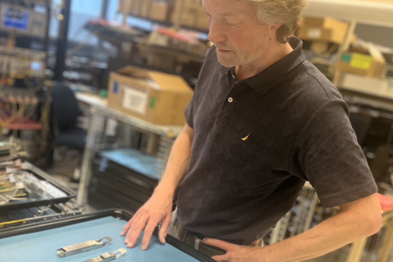
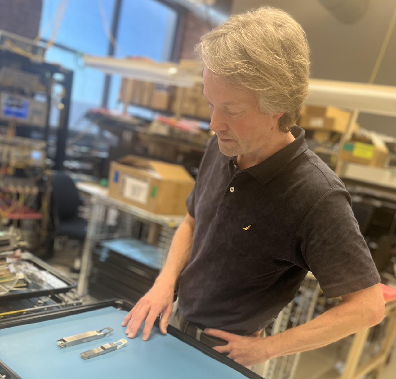
“We have all the design work done on the product, and we are taking orders,” says Bill Koss, CEO of Drut (pictured).
System architecture
The start-up’s latest building block as part of its disaggregated computing portfolio is the Photonic Resource Unit 2500 (PRU 2500) chassis that hosts up to eight double-width accelerator chips. The chassis also features Drut’s interface cards that use co-package optics to link servers to the chassis, link between the chassis directly or, for larger systems, through optical or electrical switches.
The PRU 2500 chassis supports various vendors’ accelerator chips: graphics processing units (GPUs), chips that combine general processing (CPU) and machine learning engines, and field programmable gate arrays (FPGAs).
Drut has been using third-party designs for its first-generation disaggregated server products. More recently the start-up decided to develop its own PRU 2500 chassis as it wanted to have greater design flexibility and be able to support planned enhancements.
Koss says Drut designed its disaggregated computing architecture to be flexible. By adding photonic switching, the topologies linking the chassis, and the accelerator chips they hold, can be combined dynamically to accommodate changing computing workloads.
Up to 64 racks – each rack hosting eight PRU 2500 chassis or 64 accelerator chips – can be configured as a 4096-accelerator chip disaggregated compute cluster. Four such clusters can be networked together to achieve the full 16,384 chip cluster. Drut refers to its compute cluster concept as the DynamicXcelerator virtual POD architecture.

The architecture can also be interfaced to an enterprise’s existing IT resources such as Infiniband or Ethernet switches. “This set-up has scaling limitations; it has certain performance characteristics that are different, but we can integrate existing networks to some degree into our infrastructure,” says Koss.
PRU-2500
The PRU 2500 chassis is designed to support the PCI Express 5.0 protocol. The chassis supports up to 12 PCIe 5.0 slots, including eight double-width slots to host PCIe 5.0-based accelerators. The chassis comes with two or four tFIC 2500 interface cards, discussed in the next section.
The remaining four of the 12 PCIe slots can be used for single-width PCIe 5.0 cards or Drut’s rFIC-2500 remote direct memory access (RDMA) network cards for optical-based accelerator-to-accelerator data transfers.
Also included in the PRU 2500 chassis are two large Broadcom PEX89144 PCIe 5.0 switch chips. Each PEX chip can switch 144 PCIe 5.0 lanes for a total bandwidth of 9.2 terabits-per-second (Tbps).

Co-packaged optics and photonic switching
The start-up is a trailblazer in adopting co-packaged optics. Due to the input-output requirements of its interface cards, Drut chose to use co-packaged optics since traditional pluggable modules are too bulky and cannot meet the bandwidth density requirements of the cards.
There are two types of interface cards. The iFIC 2500 is added to the host while the tFIC 2500 is part of the PRU 2500 chassis, as mentioned. Both cards are a half-length PCIe Gen 5.0 card and each has two variants: one with two 800-gigabit optical engines to support 1.6Tbps of I/O and one with four engines for 3.2Tbps I/O. It should be noted that these cards are used to carry PCIe 5.0 lanes, each lane operating at 32 gigabits-per-second (Gbps) using non-return-to-zero (NRZ) signalling.
The cards interface to the host server and connect to their counterparts in other PRU 2500 chassis. This way, the server can interface with as accelerator resources across multiple PRU 2500s.
Drut uses co-packaged optics engines due to their compact size and superior bandwidth density compared to traditional pluggable optical modules. “Co-package optics give us a high amount of density endpoints in a tiny physical form factor,” says Koss.
The co-packaged optics engines include integrated lasers rather than using external laser sources. Drut has already sourced the engines from one supplier and is also waiting on sources from two others.
“The engines are straight pipes – 800 gigabits to 800 gigabits,” says Koss. “We can drop eight lasers anywhere, like endpoints on different resource modules.”

Drut also uses a third-party’s single-mode-fibre photonic switch. The switch can be configured from 32×32 up to 384×384 ports. Drut will talk more about the photonic switching aspect of its design later this year.
The final component that makes the whole system work is Drut’s management software, which oversees the system’s traffic requirements and the photonic switching. The complete system architecture is shown below.

More development
Koss says being an early adopter of co-package optics has proven to be a challenge.
The vendors are still at the stage of ramping up volume manufacturing and resolving quality and yield issues. “It’s hard, right?” he says,
Koss says WDM-based co-packaged optics are 18 to 24 months away. Further out, he still foresees photonic switching of individual wavelengths: “Ultimately, we will want to turn those into WDM links with lots of wavelengths and a massive increase in bandwidth in the fibre plant.”
Meanwhile, Drut is already looking at its next PRU chassis design to support the PCIe 6.0 standard, and that will also include custom features driven by customer needs.
The chassis could also feature heat extraction technologies such as water cooling or immersion cooling, says Koss. Drut could also offer a PRU filled with CPUs or a PRU stuffed with memory to offer a disaggregated memory pool.
“A huge design philosophy for us is the idea that you should be able to have pools of GPUs, pools of CPUs, and pools of other things such as memory,” says Koss. “Then you compose a node, selecting from the best hardware resources for you.”
This is still some way off, says Koss, but not too far out: “Give us a couple of years, and we’ll be there.”
The long game: Acacia's coherent vision
In 2007, Christian Rasmussen made a career-defining gamble. After attending a conference featuring presentations on coherent optical transmission, he returned home, consulted his family, and quit his job at Mintera, then an optical networking equipment maker.
The technology he’d seen discussed promised to solve the transmission impairments associated with direct-detection-based optical transmission – chromatic dispersion and polarisation mode dispersion – that had stymied optical transport to go beyond 40 gigabits-per-second (Gbps).
“We came back and were completely excited that there was a technology that addressed all the problems that we had experienced firsthand,” says Rasmussen, now Chief Technology Officer at Acacia.
His bet paid off. Acacia which he helped co-found in 2009, had a successful IPO in 2016 and would later be acquired by Cisco Systems for $4.5 billion in 2021.
Unfolding coherent optics
Increasing the baud rate has proved spectacularly successful in accommodating traffic growth in the network and reducing transport costs measured in dollar-per-bit.
In 2009, coherent modems operated around 32 gigabaud (GBd) for 100 gigabit-per-second (Gbps) wavelength transmissions. By 2024, the symbol rate has reached 200GBd, enabling 1.6 terabit-per-second (Tbps) wavelengths.
Is the priority still to keep upping the symbol rate of a single carrier when designing next-generation coherent modems?
“We are not just saying that increasing baud rate is right,” says Rasmussen. The fundamental goal is reducing optical transport’s cost and power consumption. “Increasing the baud rate is generally the right approach to achieve that goal but it’s always to a certain degree.”
Acacia’s focus from the beginning has been on integrating the components that make up the coherent modem. The resulting modem need not be expensive and can deliver higher speed and extra bandwidth economically while meeting the power consumption target, he says.
“Until now, we feel that increasing the baud rate has been the right approach,” says Rasmussen. “The question will be how frequently you can go up in baud rate, now that developments are expensive.”
Given the rising cost of developing coherent modems, upping the baud rate only makes sense if designers can double it with each new design, he says. Increasing the baud rate by 30 or 40 percent is too small a return, given the development effort and the costs involved.
That implies Acacia’s follow-on high-end coherent modem will have a symbol rate of around 280GBd.
Acacia’s coherent modules
Acacia’s Coherent Interconnect Module 8 (CIM 8), launched in 2021, was the industry’s first single-carrier 1.2Tbps pluggable module. The module operates at a 140GBd symbol rate.
At ECOC 2024, the company showcased its 800 gigabit ZR+ OSFP pluggable modules, featuring the Delphi coherent DSP implemented in 4nm CMOS process.
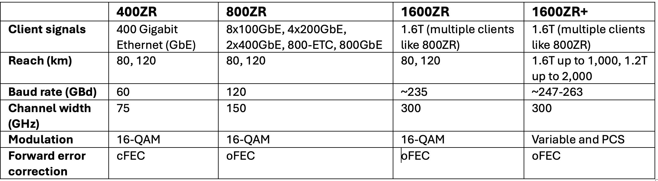
The module supports up to 131GBd and implements interoperable probabilistic constellation shaping. The Acacia module has C-band and L-band variants and supports ultra-long-haul distances when sending 400Gbps over a single carrier (see Table).

Challenges and opportunities
The path forward presents challenges and opportunities. There are several design considerations when developing a coherent DSP ASIC.
One is choosing what CMOS process to use. Considerations include cost – the smaller the geometry the more expensive the design, the transistors’ switching speed, whether the chip’s resulting power consumption is acceptable, and the CMOS process’s maturity. If the process is under development, what confidence is there that it will deliver the promised performance once the ASIC design is completed and ready for manufacturing?
The state-of-the-art CMOS process used for coherent DSPs is 3nm. Ciena’s 200GBd WaveLogic 6e is the first coherent DSP to ship using a 3nm CMOS process. Rasmussen is confident that a 3nm CMOS process can achieve at least a 250GBd symbol rate.
Another consideration is to ensure that the DSP’s analogue-to-digital converters (ADCs) and digital-to-analogue converters (DACs) can achieve the required sampling speed and quality. Typically, the ADC sample at 1.1x-1.2x the baud rate, which, for a 250GBd symbol rate, equates to the order of 300 giga-samples a second (GS/s). Achieving such speeds is exceptionally challenging.
Some research is exploring other ways to keep boosting converter sampling speed. One idea is to split the converter’s design between the DSP and a higher-bandwidth III-V material used for the driver or receiver circuitry.
Rasmussen stresses that the key is to keep the ADCs and DACs in CMOS as a part of the DSP. “Once you start going there [splitting the DAC and ADC designs], you start risking your cost and power advantage of the single-carrier approach,” he says.
Acacia timeline
- 2007: Rasmussen attends pivotal conference on coherent transmission
- 2009: Acacia founded; 32GBd coherent modems achieve 100Gbps
- 2014: Acacia is first to ship samples of a coherent pluggable 100G CFP module and announced the industry’s first 100G coherent transceiver in a single silicon photonics integrated circuit package
- 2021: Cisco acquires Acacia for $4.5 billion
- 2021: Launch of CIM 8 (140GBd, 1.2Tbps)
- 2024: Acacia showcases its 800ZR+ OSFP module
Team-oriented approach
As CTO, Rasmussen emphasises the importance of working with colleagues to make decisions. “I’m very passionate about this: team-oriented decision-making,” he says. His role involves extensive conversations with product managers and colleagues that interact with customers to understand market needs, alongside technical discussions and conference attendance to guide technology development.
This collaborative approach has shaped Acacia’s integration strategy as well as the company becoming more vertically integrated. “Owning the whole stack so you always have everything in control,” as Rasmussen puts it, has proven crucial to their success.

From Denmark to Cisco
Rasmussen’s journey began in Denmark, where he completed his electrical engineering degree and doctorate in optical communications before moving to Boston. There, he joined Benny Mikkelsen, now Acacia’s senior vice president and general manager, at Mintera, where they grappled with the limitations of pre-coherent optical systems.
The struggle with 40Gbps direct-detect optical transport systems ultimately led to that pivotal moment in 2007. “It did not make much commercial sense to struggle so much to get to 40 gigabits,” Rasmussen recalls. When coherent transmission emerged as a solution, he and his colleagues seized the opportunity, despite the industry’s post-dot-com bubble and the 2008 financial crisis.
He began working with Mikkelsen and Mehrdad Givehchi on business plans and developing the technology. “Digital signal processing was new to us, so there was a lot of stuff to learn,” he says.
After being turned down by numerous venture capital firms, one – Matrix Parners- backed the Acacia team, which also received corporate funding from OFS, part of Furukawa Electric.
Beyond Technology
Outside the lab, Rasmussen finds balance in gardening, appreciating its immediate rewards compared to the years-long cycle of DSP design. “It’s nice to do something where you can see the immediate result of your work,” he says.
His interests also extend to reading. He recommends “Right Hand, Left Hand” by Chris McManus, praising its exploration of symmetry in nature, and “The Magic of Silence” by Florian Illies, which examines the enduring relevance of painter Caspar David Friedrich.
Looking ahead, Rasmussen remains optimistic about the industry’s innovative capacity.
He says that semiconductor foundries do not tend to publicise their CMOS transistors’ switching frequency, but it is already above 500GHz and approaching 1,000GHz. This suggests that a DSP supporting a baud rate of 400GBd will be possible. And four to five years hence, two more generations of CMOS after 3nm are likely. This all suggests that a further doubling of baud rate to 500GBd is feasible.
“Just look at the record of innovation at Acacia and other companies in the industry; people keep coming up with solutions,” says Rasmussen.

Steve Alexander's 30-Year Journey at Ciena
After three decades of shaping optical networking technology, Steve Alexander is stepping down as Ciena’s Chief Technology Officer (CTO).
His journey, from working on early optical networking systems to helping to implement AI as part of Ciena’s products, mirrors the evolution of telecommunications itself.
The farewell
“As soon as you say, ‘Hey guys, you know, there’s an end date’, certain things start moving,” says Alexander reflecting on his current transition period. “Some people want to say goodbye, others want more of your time.”
After 30 years of work, the bulk of it as CTO, Alexander is ready to reclaim his time, starting with the symbolic act of shutting down Microsoft Outlook.
“I don’t want to get up at six o’clock and look at my email and calendar to figure out my day,” he says.
His retirement plans blend the practical and the fun. The agenda includes long-delayed home projects and traveling with his wife. “My kids gave us dancing lessons for a Christmas present, that sort of thing,” he says with a smile.
Career journey
The emergence of the erbium-doped fibre amplifier shaped Alexander’s career.
The innovation sparked the US DARPA’s (Defense Advanced Research Projects Agency) interest in exploring all-optical networks, leading to a consortium of AT&T, Digital Equipment Corp., and MIT Lincoln Labs, where Alexander was making his mark.
“I did coherent in the late 80s and early 90s, way before coherent was cool,” he recalls. The consortium developed a 20-channel wavelength division multiplexing (WDM) test bed, though data rates were limited to around 1 Gigabit-per-second due to technology constraints.
“It was all research with components built by PhD students, but the benefits for the optical network were pretty clear,” he says.
The question was how to scale the technology and make it commercial.
A venture capitalist’s tip about a start-up working on optical amplifiers for cable TV led Alexander to Ciena in 1994, where he became employee number 12.
His first role was to help build the optical amplifier. “I ended up doing what effectively was the first kind of end-to-end link budget system design,” says Alexander. “The company produced its first product, took it out into the industry, and it’s been a great result since.”
The CTO role
Alexander became the CTO at Ciena at the end of the 1990s.
A CTO needs to have a technology and architecture mindset, he says, and highlights three elements in particular.
The first includes such characteristics as education and experience, curiosity, and imagination. Education is essential, but over time, it is interchangeable with experience. “They are fungible,” says Alexander.
Another aspect is curiosity, the desire to know how things work and why things are the way they are. Imagination refers to the ability to envisage something different from what it is now.
“One of the nicest things about the engineering skill set, whatever the field of engineering you’re in, is that with the right tools and team of people, once you have the idea, you can make it happen,” says Alexander.
Other aspects of the CTO’s role are talking, travelling, trouble-making, and tantrum throwing. “Trouble-making comes from the imagination and curiosity, wanting to do things maybe a little bit different than the status quo,” says Alexander.
And tantrums? “When things get really bad, and you just have to make a change, and you stomp your foot and pound the table,” says Alexander.
The third aspect a CTO needs is being in the “crow’s nest”, the structure at the top of a ship’s mast: “The guy looking out to figure out what’s coming: is it an opportunity? A threat? And how do we navigate around it,” says Alexander.
Technology and business model evolution
Alexander’s technological scope has grown over time, coinciding with the company’s expanding reach to include optical access and its Blue Planet unit.
“One of the reasons I stayed at the company for 30 years is that it has required a constant refresh,” says Alexander. “It’s a challenge because technology expands and goes faster and faster.”
His tenure saw the transformation from single-channel Sonet/ SDH to 16-channel WDM systems. But Alexander emphasizes that capacity wasn’t the only challenge.
“It’s not just delivering more capacity to more places, the business model of the service providers relies on more and more levels of intelligence to make it usable,” he says.
The gap between cloud operators’ agility and that of the traditional service providers became evident during Covid-19. “The reason we’re so interested in software and Blue Planet is changing that pretty big gap between the speed at which the cloud can operate and the speed at which the service provider can operate.”
Coherent optics
Ciena is shipping the highest symbol rate coherent modem, the WaveLogic 6 Extreme. This modem operates at up to 200 gigabaud and can send 1.6 terabits of data over a single carrier.
Alexander says coherent optics will continue to improve in terms of baud rate and optical performance. But he wonders about the desired direction the industry will take.
He marvels at the success of Ethernet whereas optical communications still has much to do in terms of standardization and interoperability.
There’s been tremendous progress by the OIF and initiatives such as 400ZR, says Alexander: “We are way better off than we were 10 years ago, but we’re still not at the point where it’s as ubiquitous and standardised as Ethernet.”
Such standardisation is key because it drives down cost.
“People have discussed getting on those Ethernet cost curves from the photonic side for years. But that is still a big hurdle in front of us,” he says.
AI’s growing impact
It is still early days for AI, says Alexander, but there are already glimmers of success. Longer term, the impact will likely be huge.
AI is already having an impact on software development and on network operations.
Ciena’s customers have started by looking to do simple things with AI, such as reconciling databases. Service providers have many such data stores: an inventory database, a customer database, a sales database, and a trouble ticket database.
“Sometimes you have a phone number here, an email there, a name elsewhere, things like a component ID, all these different things,” he says. ”If you can get all that reconciled into a consistent source of knowledge, that’s a huge benefit.”
Automation is another area that typically requires using multiple manual systems. There are also research papers appearing where AI is being used to design photonic components delivering novel optical performance.
AI will also impact the network. Humans may still be the drivers but it will be machines that do the bulk of the work and drive traffic.
“If you are going to centralize learning and distributed inferencing, it’s going to have to be closer to the end user,” says Alexander.
He uses a sports application as an example as to what could happen.
“If you’re a big soccer/ football fan, and you want to see every goal scored in every game that was broadcast anywhere in the world in the last 24 hours, ranked in a top-10 best goals listing, that’s an interesting task to give to a machine,” he says.
Such applications will demand unprecedented network capabilities. Data will need to be collected, and there will be a lot of machine-to-machine interactions to generate maybe a 10-minute video to watch.
“If you play those sorts of scenarios out, you can convince yourself that yes, networks are going to have lots of demand placed on them.”
Personal Reflection
While Alexander won’t miss his early morning Outlook checks, he’ll miss his colleagues and the laboratory environment.
A Ciena colleague, paying tribute to Alexander, describes him as being an important steward of Ciena’s culture. “He always has lived by the credo that if you care for your people, people will care for the company,” he says.
Alexander plans to keep up with technology developments, but he acknowledges that losing the inside view of innovation will be a significant change.
When people have asked him why he has stayed at Ciena, his always has answered the same way: “I joined Ciena for the technology but I stayed because of the people.”
Further Information
Ciena’s own tribute, click here

OIF adds a short-reach design to its 1600ZR/ ZR+ portfolio
The OIF (Optical Internetworking Forum) has broadened its 1600-gigabit coherent optics specification work to include a third project, complementing the 1600ZR and 1600ZR+ initiatives.
The latest project will add a short-reach ‘coherent-lite’ digital design to deliver a reach of 2km to 20km and possibly 40km with a low latency below 300ns
The low latency will suit workloads and computing resources distributed across data centres.
“The coherent-lite is more than just the LR (long reach) work that we have done [at 400 gigabits and 800 gigabits],” says Karl Gass, optical vice chair of the OIF’s physical link layer (PLL) working group, adding that the 1600-gigabit coherent-lite will be a distinct digital design.
Doubling the data rate from 800 gigabits to 1600 gigabits is the latest battle line between direct-detect and coherent pluggable optics for reaches of 2km to 40km.
At 800 gigabits, the OIF members debated whether the same coherent digital signal processor would implement 800ZR and 800-gigabit LR. Certain OIF members argued that unless a distinct, coherent DSP is developed, a coherent optics design will never be able to compete with direct-detect LR optics.
“We have that same acknowledgement that unless it’s a specific design for [1600 gigabit] coherent-lite, then it’s not going to compete with the direct detect,” says Gass.
OIF’s 1600-gigabit specification work
The OIF’s 1600-gigabit roadmap has evolved rapidly in the last year.
In September 2023, the OIF announced the 1600ZR project to develop 1.6-terabit coherent optics with a reach of 80km to 120km. In January 2024, the OIF announced it would undertake a 1600ZR+ specification, an enhanced version of 1600ZR with a reach of 1,000km.
The OIF’s taking the lead in ZR+ specification work is a significant shift in the industry, promising industry-wide interoperability compared to the previous 400ZR+ and 800ZR+ developments.
Now, the OIF has started a third 1600-gigabit coherent-lite design.
1600ZR development status
Work remains to complete the 1600ZR Implementation Agreement, the OIF’s specification document. However, member companies have agreed upon the main elements, such as the framing schemes for the client side and the digital signal processing and using oFEC as the forward error correction scheme.
oFEC is a robust forward error correction scheme but adds to the link’s latency. It has also been chosen as the forward error correction scheme for 1600ZR. The OIF members want the ‘coherent-lite’ version to use a less powerful forward error correction to achieve lower latency.
The 1600ZR symbol rate chosen is around 235 gigabaud (GBd), while the modulation scheme is 16-ary quadrature amplitude modulation (16-QAM). The specified reach will be 80km to 120km. (See table below.)
The members will likely agree on the digital issues this quarter before starting the optical specification work. Before completing the Implementation Agreement, members must also spell out interoperability testing.
1600ZR+ development status
The 1600ZR+ work still has some open questions.
One is whether members choose a single carrier, two sub-carriers, or four to achieve the 1,000km reach. The issue is equalisation-enhanced phase noise (EEPN), which imposes tighter constraints on the received laser. Using sub-carriers, the laser constraints can be relaxed, enabling more suppliers. The single-carrier camp argues that sub-carriers complicate the design of the coherent digital signal processor (DSP).
The workgroup members have also to choose the probabilistic constellation shaping to use. Probabilistic constellation shaping gain can extend the reach, but it can also reduce the symbol rate and, hence, the bandwidth specification of the coherent modem’s components.
The symbol rate of the 1600ZR+ is targeted in the range of 247GBd to 263GBd.
Power consumption
The 1600ZR design’s power consumption was hoped to be 26W, but it is now expected to be 30W or more. The 1600ZR+ is expected to be even higher.
The coherent pluggable’s power consumption will depend on the CMOS process that the coherent DSP developers choose for their 1600ZR and 1600ZR+ ASIC designs. Will they choose the state-of-the-art 3nm CMOS process or wait for 2nm or even 1.8nm to become available to gain a design advantage?
Timescales
The target remains to complete the 1600ZR Implementation Agreement document quickly. Gass says the 1600ZR and 1600ZR+ Implementation Agreements could be completed this year, paving the way for the first 1600ZR/ZR+ products in 2026.
“We are being pushed by customers, which isn’t a bad thing,” says Gass.
The coherent-lite design will be completed later given that it has only just started. At present, the OIF will specify the digital design and not the associated optics, but this may change, says Gass.