
Tomahawk 6: The industry’s first 100-terabit switch chip

Part 2: Data Centre Switching
Peter Del Vecchio, product manager for the Tomahawk switch family at Broadcom, outlines the role of the company’s latest Tomahawk 6 Ethernet switch chip in AI data centres.
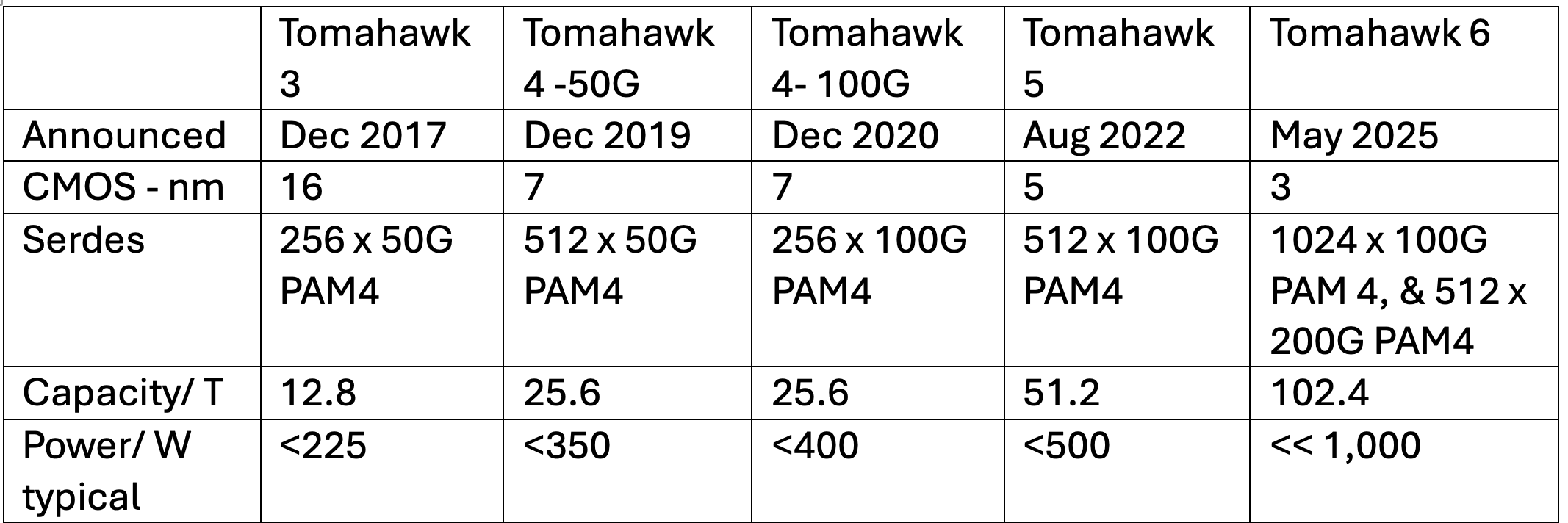
Broadcom is now shipping samples of its Tomahawk 6, the industry’s first 102.4-terabit-per-second (Tbps) Ethernet switch chip. The chip highlights AI’s impact on Ethernet networking switch chip design since Broadcom launched its current leading device, the 51.2-terabit Tomahawk 5. The Tomahawk 6 is more evolutionary, rather than a complete change, notes Del Vecchio. The design doubles bandwidth and includes enhanced networking features to support AI scale-up and scale-out networks.
Nvidia is the only other company that has announced a 102.4 terabit switch, and it’s scheduled for production in 2026,” says Bob Wheeler, analyst at large at market research firm LightCounting, adding that Nvidia sells switches, not chips.
Multi-die architecture
The Tomahawk 6 marks a shift from the monolithic chip design of the Tomahawk 5 to a multi-die architecture.
The 102.4 terabit Tomahawk 6 comes in two versions. One has 512 input-output lanes – serialisers/ deserialisers (serdes) – operating at 200-gigabit using 4-level pulse amplitude modulation signalling (PAM-4). The other Tomahawk 6 version has 1,024 serdes, each using 100-gigabit PAM-4.
“The core die is identical between the two, the only difference are the chiplets that are either for 100 gig or 200 gig PAM-4,” says Del Vecchio. The core die hosts the packet processing and traffic management logic.
The chip uses a 3nm CMOS process node, which improves power efficiency compared to the 5nm CMOS Tomahawk 5.
Broadcom does not quote exact power figures for the chip. “The Tomahawk 6 is significantly less than one watt per 100 gigabits-per-second, well below 1,000 watts,” says Del Vecchio. In contrast, the Tomahawk 5 consumes less than 512 watts.
AI networking: Endpoint-scheduled fabrics
The Tomahawk 6 chip is designed for AI clusters requiring near-100 per cent network utilisation.
“With previous data centre networks, it was unusual that the networks would be loaded to more than 60 to 70 per cent utilisation,” says Del Vecchio. “For AI, that’s unacceptable.”
The chip supports endpoint-scheduled fabrics, where traffic scheduling and load balancing occur at the endpoints to ensure the traffic is efficiently distributed across the network. An endpoint could be a network interface card (NIC) or an AI accelerator interface.
This contrasts with Broadcom’s other switch chip family, the Jericho 3-AI and the Ramon, which is designed for switch-scheduled fabrics. Here, the switch chip handles the networking and packet spraying, working alongside simpler end-point hardware.
The type of switch chip used – endpoint schedule or switch scheduled – depends on the preferences of service providers and hyperscalers. Broadcom says there is demand for both networking approaches.
The Tomahawk 6 uses Broadcom’s latest cognitive routing suite and enhanced telemetry to address the evolving AI traffic patterns.
The market shifted dramatically in 2022, says Del Vecchio, with demand moving from general data centre networking to one focused on AI’s needs. The trigger was the generative AI surge caused by the emergence of ChatGPT in November 2022, after the Tomahawk 5 was already shipping.
“There was some thought of AI training and for inference [with the Tomahawk 5], but the primary use case at that point was thought to be general data centre networks,” says Del Vecchio.
Wide and flat topologies
Tomahawk 6 supports two-tier networks connecting up to 128,000 AI accelerator chips, such as graphic processor units (GPUs). This assumes 200 gigabits per endpoint, which may be insufficient for the I/O requirements of the latest AI accelerator chips.
To achieve higher bandwidth per end-point – 800 gigabit or 1.6 terabit – multiple network planes are used in parallel, each adding 200 gigabits. This way, Broadcom’s design avoids adding an extra third tier of network switching.
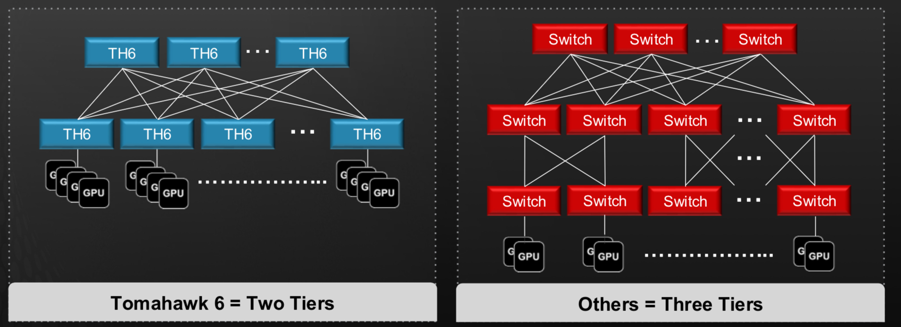
“Rather than having three tiers, you have multiple networking planes, say, eight of those in parallel,” says Del Vecchio.Such a wide-and-flat topology minimises latency and simplifies congestion control, which is critical for AI workloads. “Having a two-tier network versus a three-tier network makes congestion control much easier,” he says.
Tomahawk 6’s enhanced adaptive routing and load balancing features caters to AI’s high-utilisation demands. The aim is to try to keep the port speed low, to maximise the radix, says Del Vecchio, contrasting AI networks with general data centres, where higher 800-gigabit port speeds are typical.
Scale-Up Ethernet
The above discussion refers to the scale-out networking approach. For scale-up networking, the first hop between the AI accelerator chips, the devices are densely interconnected using multiple lanes — four or eight 200-gigabit lanes — to achieve higher bandwidth within a rack.
Broadcom has taken a different approach to scale-up networking than other companies. It has chosen Ethernet rather than developing a proprietary interface like Nvidia’s NVlink or the industry-backed UALink.
Broadcom has released its Scale-Up Ethernet (SUE) framework, which positions Ethernet as a unified solution for scale-up networks and which it has contributed to the Open Compute Project (OCP).

SUE supports large-scale GPU clusters. “You can do 512 XPUs in a scale-up cluster, connected in a single hop,” says Del Vecchio. SUE’s features include link-level retry, credit-based flow control, and optimised headers for low-latency, reliable transport.
“There is no one-size-fits-all for scale-up,” says Wheeler. “For example, Google’s ICI [inter chip interconnect] is a remote direct memory access (RDMA) based interconnect, more like Ethernet than UALink or NVLink,” says Wheeler. “There will likely be multiple camps.”
Broadcom chose Ethernet for several reasons. “One is you can leverage the whole Ethernet ecosystem,” says Del Vecchio, who stresses it results in a unified toolset for front-end, back-end, and scale-up networks.
SUE also aligns with hyperscaler preferences for interchangeable interfaces. “They’d like to have one unified technology for all that,” says Del Vecchio.
Del Vecchio is also a Ultra Ethernet Consortium (UEC) steering committee member. The UEC focuses on scale-out for its 1.0 specification, which is set for public release soon.
Link-level retry (LLR) and credit-based flow control (CBFC) are already being standardised within UEC, says Del Vecchio, and suggests that there will also be scale-up extensions which will benefit Broadcom’s SUE approach.
Interconnects
Tomahawk 6 supports diverse physical interconnects, including 100-gigabit and 200-gigabit PAM-4 serdes and passive copper links up to 2 meters, enabling custom GPU cluster designs.

“There’s a lot of focus on these custom GPU racks,” says Del Vecchio, highlighting the shift from generic pizza-box switches to highly engineered topologies.
The goal is to increase the power to each rack to cram more AI accelerator chips, thereby increasing the degree of scale-up using copper interconnect. Copper links could be used to connect two racks to further double scale-up capacity.
Co-packaged optics: Enhancing reliability?
Co-packaged optics (CPO) has also become a design feature of switch chips. The Tomahawk 6 will be Broadcom’s third-generation switch chip that will also be offered with co-packaged optics.
“People are seeing how much power is going into the optics for these GPU racks,” says Del Vecchio. Co-packaged optics eliminates retimers and DSPs, reducing latency and burst errors
Broadcom and hyperscalers are currently investigating another key potential benefit of co-packaged optics. “There are indications that you wind up with significantly fewer link flaps,” he said. A link flap refers to an link instability.
Unlike pluggable optics, which introduce burst errors via DSPs, co-packaged optics offers random Gaussian noise, which is better suited for forward error correction schemes. “If you have an end-to-end CPO link, you have much more random errors,” he explained.
This suggests that using co-packaged optics could benefit the overall runtime of massive AI clusters, a notable development that, if proven, will favour the technology’s use. “We expect the Tomahawk 6 Davisson co-packaged optics version to follow Tomahawk 6 production closely,” says LightCounting’s Wheeler.
Design challenges
Tomahawk 6’s development required overcoming significant hurdles.
Packaging over 1,000 serdes was one. “There were no packages on the market anywhere near that size,” says Del Vecchio, emphasising innovations in controlling warpage, insertion loss, and signal integrity. Del Vecchio also highlights the complexity of fanning out 1,000 lanes. The multi-die design required low-latency, low-power chip-to-chip interfaces, with Broadcom using its experience developing custom ASICs.
Traffic management structures, like the Memory Management Unit (MMU), have also seen exponential complexity increases. “Some structures are 4x the complexity,” says Del Vecchio.
The multi-die design demanded efficient chip-to-chip interfaces, while packaging 1,000 serdes lanes required signal integrity and manufacturability innovations. “We spent a lot of time on the packaging technology,” he added.
Meanwhile, using architectural optimisations, such as automatic clock gating and efficient serdes design, improved power efficiency. What about the delay in announcing the latest Tomahawk switch chip compared to the clock-like 2-year launch date gaps of previous Tomahawk chips? (See table above.)
Del Vecchio says the delay wasn’t due to a technical issue or getting access to a 3nm CMOS process. Instead, choosing the right market timing drove the release schedule.
Broadcom believes it has a six-month to one-year lead on competing switch chip makers.
Production and market timing
Tomahawk 6 samples are now shipping to hyperscalers and original equipment manufacturers (OEMs). Production is expected within seven months, matching the timeline achieved with the Tomahawk 5. “We feel confident there is no issue with physical IP,” says Del Vecchio, based on the work done with Broadcom’s test chips and verification suites.
The simultaneous availability of 100-gigabit and 200-gigabit SerDes versions of the latest switch chip reflects AI’s bandwidth demands.
“There is such a huge insatiable demand for bandwidth, we could not afford the time delay between the 100-gig and 200-gig versions,” says Del Vecchio.
Oriole’s fast optical reconfigurable network
- Start-up Oriole Networks has developed a photonic network to link numerous accelerator chips in an artificial intelligence (AI) data centre.
- The fast photonic network is reconfigurable every 100 nanoseconds and is designed to replace tiers of electrical switches.
- Oriole says its photonic networking saves considerable power and ensures the network is no longer a compute bottleneck.
In a London office bathed in spring sunlight, the team from Oriole Networks, a University College London (UCL) spin-out, detailed its vision for transforming AI and high-performance computing (HPC) data centres.
Oriole has developed a networking solution, dubbed Prism, that uses fast reconfigurable optical circuit switches to replace the tiers of electrical packet switches used to connect racks of AI processors in the data centre.
Electrical switches perform a crucial role in the data centre by enabling the scaling of AI computers comprising thousands of accelerator chips. Such chips – graphics processor units (GPUs), tensor processor units (TPUs), or more generically xPUs – are used to tackle large AI computational workloads.
The workloads include imprinting learning onto large AI models or performing inferencing once the AI model is trained, where it shares its knowledge when prompted.
Oriole’s novel network is based on optical circuit switches that can switch rapidly in response to changes in the workload, allocating the xPU resources as required. Electrical switches already do this very well.
Origins

Founded in 2023, Oriole builds on over a decade of research work by Georgios Zervas and his research team at UCL.
The start-up has raised $35 million, including a $22 million Series A led by investment firm Plural’s Ian Hogarth, a technology entrepreneur and Chair of the UK’s AI Security Institute.
The company, now 50-strong, has two UK offices—one in London and a site in Paignton—and one in Palo Alto.
Oriole’s team blends photonics expertise, including Paignton’s former Lumentum coherent transceiver group and networking talent from Intel’s former Altera division west of London, with expertise in programmable logic design work addressing hyperscalers’ needs.
AI data centre metrics
Power is a key constraint limiting the productivity of an AI data centre.
“You can only get so much power to a data centre site,” says Joost Verberk, vice president, business development and marketing at Oriole. “Once that is determined, everything else follows; the systems and networking must be as power efficient as possible so that all the power can go to the GPUs.”

Oriole highlights two metrics Nvidia’s Jensen Huang used at the company’s recent GTC event to quantify AI data centre efficiency.
One is tokens per second per megawatt (tokens/s/MW). Tokens are data elements, such as a portion of a word or a strip of pixels, part of a digital image, that are fed to or produced by an AI model. The more tokens created, the more productive the data centre.
The second metric is response speed, measured in tokens per second (tokens/s), which gauges latency (speed of response).
Oriole says these two metrics are not always aligned, but the goal is to use less power while producing more tokens faster.
Discussing tokens implies that the data centre’s hardware is used for inference. However, Oriole stresses that training AI models for less power is also a goal. Oriole’s optical networking solution can be applied to both inference and training.
Going forward, only a handful of companies, such as hyperscalers, will train the largest AI models. Many smaller-sized AI clusters will be deployed and used for inference.
“By 2030, 80 per cent of AI will be inferencing,” says James Regan, CEO of Oriole.
Networking implications
Inferencing, by its nature, means that the presented AI tasks change continually. One implication is that the networking linking the AI processors must be dynamic: grabbing processors for a given task and releasing them on completion.
George Zervas, Oriole’s CTO, points out that while Nvidia uses the same GPU for training and inferencing, Google’s latest TPU, Ironwood, has inferencing enhancements. Google also has AI computing clusters dedicated to inference jobs.
Amazon Web Services, meanwhile, has separate accelerator chips for inferencing and training. The two processors have different interconnect bandwidth requirements (input-output, or I/O), with the inferencing processor’s requirement being lower.
For training, the data exchange between the processors/xPUs, depending on how the task is parallelised, is highly predictable. “You can create a series of optical short-lasting circuits that minimise collective communication time,” says Zervas. However, the switches must be deterministic and synchronous. “You should not have [packet] queues,” he says.
Inferencing, which may access many AI ‘mixture of experts’ models, requires a more dynamic system. “Different tokens will go to different sets of experts, spread across the xPUs”, says Zervas. “Sometimes, some xPUs batch the queries and then flush them out.”
The result is non-deterministic traffic, getting closer to the traffic patterns of traditional Cloud data centres. Here, the network must be reconfigured quickly, in hundreds of nanoseconds.
“What we say is that a nanosecond-speed optical circuit switch has a place wherever any electrical packet switch has a place,” says Zervas. It’s still a circuit switch, stresses Zervas, even at such fast switching speeds, since there is a guaranteed path between two points. This is unlike ‘best effort’ traffic in a traditional electrical switch, where packets can be dropped.
“In our case, that link can last just as short as [the duration of] a packet,” says Zervas. “Our switches can be reconfigured every 100 nanoseconds.”
Once the link is established, data is sent to the other end without encountering queuing. Or, as Zervas puts it, the switching matches the granularity of packets yet has delivery guarantees that only a circuit can deliver.
Optics’ growing role in data centre networking
Currently, protocols such as Infiniband or Ethernet are used to connect racks of xPUs, commonly referred to as the scale-out network. For xPUs to talk to each other, a traditional Clos or ‘fat tree’ architecture comprising a hierarchy of electrical switches is used.
Because of the distances spanning a data centre, pluggable transceivers connect an xPU via a networking interface card to the switching network to connect to the destination network interface card and xPU.
Broadcom and Nvidia have announced electrical switches that integrate optics with silicon switches, a newer development. Using such co-packaged optics circumvents the need for pluggable optical transceivers on the front panel of an electrical switch platform.
Google has also developed its data centre architecture to include optical circuit switches instead of the top tier of large electrical switches. In such a hybrid network, electrical switches still dominate the overall network. However, using the optical layer saves cost and power and allows Google to reconfigure the interconnect between its TPU racks as it moves workloads around.
However, Google’s optical circuit switch’s configuration speed is far slower than Oriole’s, certainly not nanoseconds.
With its Prism architecture, Oriole is taking the radical step of replacing all the electrical switching, not just the top tier. The result is a flat passive optical network.

“Switching happens at the edge [of the network] and the core is fully passive; it is made just of glass,” says Verberk.
The resulting network has zero packet loss and is highly synchronous. Eliminating electrical switches reduces overall power and system complexity while delivering direct xPU to xPU high-speed connectivity.
Prism architecture
Oriole’s first announcement is the Prism architecture that hinges on three system components:
- a PCI Express (PCIe) based network interface card.
- A novel pluggable module – the XTR – includes the optical transceiver and switching.
- A photonic router that houses athermal arrayed waveguide gratings (AWGs) to route the different wavelengths of light. The router box is passive and has no electronics.

“You go optically from the GPU out to another GPU, and the only [electrical-optical] conversion that happens is at the network interface card next to each GPU,“ says Verberk.
The PCIe-based network interface card uses 800-gigabit optics and integrates with standard software ecosystems.
Built around an FPGA that includes ARM processors, the card supports protocols like Nvidia’s NCCL (Nvidia Collective Communications Library) and AMD’s RCCL Radeon Open Compute Communication Collectives Library) via plugins, ensuring compatibility with existing AI software frameworks.
The network interface card acts as a deterministic data transport, mapping collective operations used for AI computation (e.g., Message Passing Interface operations like all-reduce, scatter-gather) to optical paths with minimal latency.
The card’s scheduler maps deterministic patterns directly to wavelengths and fibres for training. At the same time, it dynamically reconfigures based on workload demands, using a standard direct memory access (DMA) engine for inference.
The XTR pluggable module is the heart of Prism’s switching capability. “Within a pluggable form factor unit, we do transmission, reception, and switching,” says Zervas.
The photonic network combines three dimensions of switching: optical wavelengths, space switching, and time slots (time-domain multiplexing).
The chosen wavelength colour is determined using a fast tunable laser.
The space switching inside the XTR pluggable refers to the selected fibre path. “You have a ribbon of fibres, and you can choose which fibres you want to go to,” says Regan.

The time aspects refer to time slots of 100 nanoseconds, the time it takes for the tunable laser to adjust to a new wavelength. Overall, rapid colour changes can be used to route data to specific nodes.
“The modulated channel can determine which communication group or cluster you can go to, and the fibre route can determine the logical rack you’re going to, and then the colour of light you’re carrying can determine the node ID within the rack,” says Zervas.
The photonic routers, passive arrayed waveguide gratings, form Prism’s core. “They’re just glass, which means they are athermal,” says Regan, highlighting their reliability and zero power consumption. These N-by-N arrayed waveguide gratings route light based on wavelength and fibre selection, acting like prisms.
“On one port, let’s say the input port, we have a colour red; if it’s red, it comes to the first output, if it’s blue, to the second, if it’s purple, to the third, etc.,” says Zervas.
Stacked racks of multiple arrayed waveguide gratings can handle large-scale clusters, maintaining a single optical hop for consistent signal-to-noise ratio and insertion loss.
“Every node to every other node goes through this only once, ensuring uniform performance across thousands of GPUs,” says Zervas.
Prism’s Power and compute efficiencies
Using an 8,000-GPU cluster example, Prism eliminates 128 leaf and 64 spine electrical switches, cutting the number of optical transceivers by 60 per cent.
For even large AI clusters of over 16,000 GPUs, a third tier of switching is typically needed. This reduces the number of transceivers by 77 per cent.
Using Prism reduces overall power, not only optical transceivers but also by removing electrical switching and the associated cooling they need.
Unlike Ethernet packet switching, Prism’s optical circuits guarantee delivery without queuing, reconfiguring every 100 nanoseconds that matches packet durations.
For training, Prism reduces communication overhead to under 1 per cent. In existing networks, it is typically tens of per cent. This means the GPUs rarely wait for data and spend their time processing.
Market and deployment strategy
Oriole targets three segments: enterprises such as financial traders, HPC users such as car makers, switch makers, and hyperscalers.
“Our potential customer base is much wider,” says Regan, contrasting with chip-level optical input-output players focusing on specific chip vendors and hyperscalers.
Prism also features an Ethernet gateway that allows integration with existing data centres, avoiding a rip-and-replace. “You could just do that in the pieces of your data centre where you need it, or where you do new builds,” says Regan.
Oriole’s roadmap includes lab demonstrations this summer, alpha hardware by early 2026, deployable products by the end of 2026, and production ramp-up in 2027. Manufacturing is outsourced to high-volume contract manufacturers.
Challenges and outlook
Convincing hyperscalers to adopt a non-standard software stack remains a hurdle. “It becomes a collaboration,” says Zervas, noting the hyperscalers’ use of proprietary protocols.
Oriole’s full-stack approach—spanning Nvidia’s CUDA libraries to photonic circuits—does set it apart.
“It’s not often you bump into a company that has deep expertise in both [photonics and computing],” says Regan, contrasting Oriole with photonics-only or computing-only competitors.
“We’re building something here,” says Regan. “We’re building a major European player for networking, for AI, and arbitrary workloads into the future.”

OFC 2025 industry reflections - Final Part

Gazettabyte has been asking industry figures for their thoughts after attending the OFC conference held in San Francisco.
In the final part, Arista’s Vijay Vusirikala and Andy Bechtolsheim, Chris Doerr of Aloe Semiconductor, Adtran’s Jörg-Peter Elbers, and Omdia’s Daryl Inniss share their learnings. Vusirikala, Doerr, and Elbers all participated in OFC’s excellent Rump Session.
Vijay Vusirikala, Distinguished Lead, AI Systems and Networks, and Andy Bechtolsheim, Chief Architect, at Arista Networks.
OFC 2025 wasn’t just another conference. The event felt like a significant momentum-gaining inflexion point, buzzing with an energy reminiscent of the Dot.com era optical boom.
This palpable excitement, reflected in record attendance and exhibitor numbers, was accentuated for the broader community by the context set at Nvidia’s GTC event held two weeks before OFC, highlighting the critical role optical technologies play in enabling next-generation AI infrastructure.
This year’s OFC moved beyond incremental updates, showcasing a convergence of foundational technologies and establishing optics not just as a supporting player but a core driver in the AI era. The scale of innovation directed towards AI-centric solutions – tackling power consumption, bandwidth density, and latency – was striking.
Key trends that stood out were as follows:
Lower Power Interconnect technologies
The overarching topic was the need for more power-efficient optics for high-bandwidth AI fabrics. Legacy data centre optics are impacting the number of GPUs that fit into a given data centre’s power envelope.
Three main strategies were presented to address the power issue.
First, whenever possible, use copper cables, which are far more reliable and cost less than optics. The limitation, of course, is copper’s reach, which at 200 gigabit-per-lane is about 1-2m for passive copper cables and 3-4m for active redriven copper cables.
Second, eliminate the traditional digital signal processor (DSP) and use linear interface optics, including Linear Pluggable Optics (LPO), Near Package Optics (NPO), and Co-Packaged Optics (CPO), all of which offer substantial (60%) power savings, lower latency, and higher reliability compared to traditional DSP solutions.
The biggest difference between linear pluggable optics and co-packaged optics is that linear pluggable optics retains the well-known operational advantages of pluggable modules: configurability, multi-vendor support, and easy field serviceability (hot-swapping at module level), compared to fixed optics like co-packaged optics, which require chassis-level RMAs (return materials authorisation). It remains to be seen whether co-packaged optics can overcome the serviceability issues.
Third, developments in a host of new technologies – advances in copper interconnects, microLED-based interconnects, and THz-RF-over-waveguides – promise even lower power consumption than current silicon photonics-based interconnect technologies.
We look forward to hearing more about these new technologies next year.
Transition from 200 gigabit-per-lambda to 400 gigabit-per-lambda
With the 200 gigabit-per-lambda optical generation just moving into volume production in 2025-26, attention has already turned to the advancement and challenges of 400 gigabit-per-lambda optical technologies for future high-speed data transmission, aiming towards 3,200 gigabit (8×400 gigabit) modules.
Several technical approaches for achieving 400 gigabit-per-lambda were discussed, including PAM-4 intensity modulation direct detection (IMDD), PAM-4 dual-polarisation, and optical time division multiplexing (OTDM). The technology choices here include indium phosphide, thin-film lithium niobate (TFLN), and silicon photonics, which are compared based on RF (radio frequency) loss, integration, cost, and high-volume readiness.
For 400 gigabit lambda optics, indium phosphide and thin-film lithium niobate are strong candidates, as silicon photonics will struggle with the high bandwidth.
At this point, it is impossible to predict which platform will emerge as the high-volume winner. Delivering power and cost-effective 400-gigabit lambda optics will require a concerted industry effort from optical component suppliers, connector suppliers, and test and measurement vendors.
Multi-core fibre
A new pain point in large AI data centres is the sheer number of fibre cables and their associated volume and weight. One way to solve this problem is to combine multiple fibre cores in a single fibre, starting initially with four cores, which would offer a 4:1 reduction in fibre count, bulk, and weight.
Hollow-core fibre
Innovation continues in the foundational fibre itself. Hollow-core fibre generated significant buzz, with its potential for lower latency and wider bandwidth attracting intense interest.
The maturing hollow-core fibre ecosystem, including cabling and interconnection progress, suggests deployments beyond niche applications like high-frequency trading may be approaching, reaching areas like distributed AI processing.
AI-driven network evolution
AI isn’t just driving network demand, it is increasingly becoming a network management tool.
Numerous demonstrations showcased AI/machine learning applications for network automation, traffic prediction, anomaly detection, predictive maintenance – e.g., analysing optical time-domain reflectometer (OTDR) traces, configuration management, and resource optimisation. This represents a fundamental shift towards more efficient, reliable, self-configuring, self-healing, and self-optimising networks.
Along with the many technical talks and tutorials, show floor demos, and customer and supplier meetings, OFC attendees also had a chance to combine technology with some light-hearted fun at the rump session.
This year’s topic was rebuilding global communication infrastructure after an alien invasion, and three teams came up with thought-provoking ideas for this theme.
Chris Doerr, CEO of Aloe Semiconductor
The best way to describe OFC 2025 is a giant Mars dust storm that raged for days. The swirling sand made it difficult to see anything clearly, and the sound was so loud you couldn’t think.
Acronyms ending in “O” were hitting you from all sides: LPO, LRO, NPO, CPO, OIO. The wind blew away sand that had buried old technologies, such as lithium niobate, electro-optic polymer, and indium-phosphide modulators, and they joined the fray.
Only now that the storm has somewhat subsided can we start piecing together what the future holds.
The main driver of the storm was, of course, artificial intelligence (AI) systems. AI requires a vast number of communication interconnects. Most interconnects, at least within a rack, are still copper. While copper keeps making incredible strides in density and reach, a fibre-optic interconnect takeover seems more and more inevitable.
The Nvidia announcements of co-packaged optics (CPO), which go beyond co-packaged optics and deserve a new name, such as optical input-output (OIO) or system-on-chip (SOC), created a great deal of excitement and rethinking. Nvidia employs a silicon interposer that significantly increases the electrical escape density and shortens the electrical links. This is important for the long-term evolution of AI computing.
The CPO/OIO/SOC doesn’t mean the end of pluggables. Pluggables still bring tremendous value with attributes such as time-to-market, ecosystem, replaceability, etc.
Most pluggables will still be fully retimed, but 100 gigabit-per-lane seems comfortable with linear pluggable optics (LPO), and 200 gigabit-per-lane is starting to accept linear receive optics (LRO).
For 200 gigabit per lane, electro-absorption modulated lasers (EMLs) and silicon photonics have comfortably taken the lead. However, for 400 gigabit per lane, which had two main demos on the show floor by Ciena and Marvell, many technologies are jockeying for position, mostly EMLs, thin-film lithium niobate (TFLN), indium phosphide, and silicon photonics.
Many companies are abandoning silicon photonics, but this author feels this is premature. There were demos at OFC of silicon photonics attaining near 400 gigabit-per-lane, and the technology is capable of it.
An important thing to remember is that the new OIO/SOC technology is silicon photonics and comes from a CMOS foundry. Putting non-CMOS materials such as thin-film lithium niobate or indium phosphide in such a platform could take years of expensive development and is thus unlikely.
In summary, OFC 2025 was very active and exciting. Significant technology improvements and innovations are needed.
The dust is far from settled, so we must continue wading into the storm and trying to understand it all.
Jörg-Peter Elbers, Senior Vice President, Advanced Technology, Standards and IPR, Adtran
OFC 2025 marked its largest attendance since 2003 with nearly 17,000 visitors, as it celebrated its 50th anniversary.
Discussions in 1975 centred around advances in fibre technology for telecommunications. This year’s hottest topic was undoubtedly optical interconnects for large-scale AI clusters.
Following an insightful plenary talk by Pradeep Sindhu from Microsoft on AI data centre architecture, sessions were packed in which co-packaged optics (CPO) and associated technologies were discussed. The excitement had been fueled by Nvidia’s earlier announcement of using co-packaged optics in its next generation of Ethernet and Infiniband switches.
The show floor featured 800 gigabit-per-second (Gbps), 1.6 terabit-per-second (Tbps), and the first 3.2Tbps interconnect demonstrations using different interface standards and technologies.
For access, 50G-PON was showcased in triple PON coexistence mode, while interest in next-generation very high-speed PON spurred the technical sessions.
Other standout topics included numerous papers on fibre sensing, stimulating discussions on optical satellite communications, and a post-deadline paper demonstrating unrepeated hollow-core fibre transmission over more than 200km.
OFC 2025 was fun too. When else do you get to reimagine communications after an alien attack, as in this year’s rump session?
No visit to San Francisco is complete without trying one of Waymo’s self-driving taxis. Having been proud of Dmitri Dolgov, Waymo’s CEO, for his plenary talk at OFC 2019, it was thrilling to see autonomous driving in action. I love technology!
Daryl Inniss, Omdia Consultant, Optical Components and Fibre Technologies
I worked on commercialising fibre technology for emerging applications at OFS – now Lightera – from 2016 to 2023. I spent the prior 15 years researching and analysing the optical components market.
Today, I see a market on the cusp of a transition due to the unabated bandwidth demand and the rise of computing architectures to support high-performance computing (HPC) and artificial intelligence (AI).
Even optical fibre, the fundamental optical communications building block, is under intense scrutiny to deliver performance suitable for the next 30 to 50 years. Options include hollow-core and multi-core fibre, two of the three fibre technologies that caught my attention at OFC 2025.
The third, polarisation-maintaining fibre arrays for co-package optics, is one part of the conference’s biggest story. OFC 2025 provided a status update on these technologies.
Hollow-core fibre
OFC’s first day hollow-core fibre workshop (S2A) illustrated its niche status and its potential to remain in this state until the fibre is standardised. The industry ecosystem was well represented at the session.
Not surprisingly, challenges highlighted and summarised by Russ Ellis, Microsoft’s Principal Cloud Network Engineer, included manufacturing, field installation, field splicing, cabling, and termination inside the data centre. These are all expected topics and well understood.
I was surprised to hear Microsoft report that the lack of an established ecosystem was a challenge, and I’ll explain why below.
Coming into OFC, the biggest market question was fibre manufacturing scalability, as most reported draws are 5km or less. Supplier YOFC put this concern to rest by showcasing a +20 km spool from a single fibre draw on the show floor. And Yingying Wang, CEO of Linfiber, reported that 50 to 100km preforms will be available this year.
In short, suppliers can scale hollow-core fibre production.
From a field performance perspective, Microsoft highlighted numerous deployments illustrating successful fibre manufacturing, cabling, splicing, termination, installation, and testing. The company also reported no field failures or outages for cables installed over five years ago.
However, to my knowledge, the hollow-core fibre ecosystem challenge is a consequence of a lack of standardisation and discussion about standardisation.
Each fibre vendor has a different fibre design and a different glass outer diameter. Microsoft’s lack-of-an-ecosystem comment mentioned above is therefore unsurprising. Only when the fibre is standardised can an ecosystem emerge, generating volumes and reducing costs,
Today, only vertically integrated players benefit from hollow-core fibre. Until the fibre is standardised, technology development and adoption will be stunted.
Multi-core fibre
I was pleasantly surprised to find multiple transceiver vendors showcasing modules with integrated fan-in/fan-out (FIFO). This is a good idea as it supports multi-core fibre adoption.
One vendor is targeting FR4 (TeraHop for 2x400G), while another is targeting DR8 (Hyper Photonix for 8x100G). There is a need to increase core density, and it is good to see these developments.
However, we are still very far from multi-core fibre commercialisation as numerous operational factors, for example, are impacted. The good news is that multi-core fibre standardisation is progressing.
Polarisation-maintaining fibre
According to Nick Psaila, Intel’s principal engineer and technology development manager, polarisation-maintaining fibre arrays remain expensive.
The comment was made at Optica’s February online Industry Meeting and verified in my follow-up conversation with Psaila.
Using an external laser source is the leading approach to deliver light for co-packaged optics, highlighting an opportunity for high-volume, low-cost polarisation-maintaining fibre arrays.
Co-packaged optics were undoubtedly the most significant topic of the show.
Coherent showcased a 3Tbps concept product of VCSELs to be used in co-packaged optics. Given that multimode fibre is used in the shortest optical connections in data centres and that VCSELs have very low power consumption, I’m surprised I’ve not heard more about their use for this application.
Testing of emerging photonic solutions for HPC and AI devices has been identified as a bottleneck. Quantifi Photonics has taken on this challenge. The company introduced an oscilloscope that provided quality results comparable to industry-leading ones and is designed for parallel measurements. It targets photonic devices being designed for co-packaged optics applications.
Multiple channels, each with wavelength-division multiplexing lasers, must be tested in addition to all the electrical channels. This is time-consuming, expensive process, particularly using existing equipment.
Polymer modulators continue to be interesting because they have high bandwidth and the potential to be inexpensive. However, reliability is their challenge. Another vendor, NLM Photonics, is targeting this application.
The many vendors offering optical circuit switches was a surprising development. I wonder if this opportunity is sufficiently large to justify the number of vendors. I’m told that numerous internet content providers are interested in the technology. Moreover, these switches may be adopted in telecom networks. This is a topic that needs continual attention, specifically regarding the requirements based on the application.
Lastly, Lightmatter provided a clear description of its technology. An important factor is the optical interposer that removes input-output connectivity from the chip’s edge, thereby overcoming bandwidth limitations.
I was surprised to learn that the laser is the company’s design, although Lightmatter has yet to reveal more.

OFC 2025 industry reflections - Part 3
Gazettabyte is asking industry figures for their thoughts after attending the OFC show in San Francisco. In the penultimate part, the contributions are from Cisco’s Bill Gartner, Lumentum’s Matt Sysak, Ramya Barna of Mixx Technologies, and Ericsson’s Antonio Tartaglia.
Bill Gartner, Senior Vice President and General Manager, Optical Systems and Optics, Cisco
There was certainly much buzz around co-packaged optics at Nvidia’s GTC event, and that carried over into OFC.
The prevailing thinking seems to be that large-scale co-packaged optics deployment is years away. While co-packaged optics has many benefits, there are challenges that need to be overcome before that happens.
Existing solutions, such as linear pluggable optics (LPO), continue to be discussed as interim solutions that could achieve close to the power savings of co-packaged optics and preserve a multi-vendor pluggable market. That development in the industry will be an intermediate solution before co-packaged optics is required.
By all accounts, IP-over-DWDM, or Routed Optical Networking as Cisco calls it, is now mainstream, enabling network operators to take advantage of the cost, space, and power savings in almost every part of the network.
Through the Openzr+ and Openroadm models, coherent pluggable usage has expanded beyond data centre interconnect (DCI) and metro applications. The subject was covered in many presentations and announcements, including several trials by Arelion and Internet2 of the new 800-gigabit ZR+ and 400-gigabit ultra-long-haul coherent pluggable. ZR and ZR+ pluggable optics now account for more than half of the coherent ports industry-wide.
I also saw some coherent-lite demonstrations, and while the ecosystem is expanding, it appears this will be a corner case for the near future.
Lastly, power reduction was another strong theme, which is where co-packaged optics, LPO, and linear retimed optics (LRO) originated. As optics, switches, routers, and GPU (graphics processor unit) servers become faster and denser, data centres cannot support the insatiable need for more power. Network operators and equipment manufacturers are seeking alternative ways to lower power, such as liquid cooling and liquid immersion.
What did I learn at OFC? Pradeep Sindhu, Technical Fellow and Corporate Vice President of Silicon with Microsoft, gave one of the plenary talks. He believes we should stop racing to higher lane speeds because it will compromise scale. He believes 200 gigabits per second (Gbps) is a technology sweet spot.
As for show surprises, the investor presence was markedly larger than usual, a positive for the industry. With almost 17,000 people attending OFC this year and AI driving incremental bandwidth that optics will serve, you could feel the excitement on the show floor.
We’re looking forward to seeing what technologies will prevail in 2026.
Matt Sysak, CTO, Cloud and Networking Platform at Lumentum.
The industry spotlight at OFC was on next-generation data centre interconnects and growing AI-driven bandwidth demands.
Several suppliers demonstrated 400 gigabit-per-lane optics, with Lumentum showcasing both 450 gigabit-per-second (Gbps) indium phosphide Mach-Zehnder and 448 gigabit-per-lane externally modulated laser (EML) technologies.
In long-haul networking, the continued expansion of data centre traffic across longer fibre spans drives demand for high-capacity solutions such as 800G ZR C+L band transceivers. I learned at the show that the focus has shifted from incremental upgrades to building fundamentally new network layers capable of supporting AI workloads at scale. Conversations around innovations such as 400-gigabit DFB Mach-Zehnder lasers and advancements in optical circuit switches made it clear that the industry is driving innovation across every network layer.
One of the biggest surprises was the surge in optical circuit switch players. The core technology has expanded beyond traditional micro-electro-mechanical systems (MEMS) to include liquid crystal and silicon photonics approaches. There is clearly growing demand for high-radix, low-power optical interconnects to address rising data centre power consumption.
With our proven expertise in MEMS and the ability to scale port counts with low insertion loss, we believe Lumentum’s optical circuit switch offers clear advantages over competing technologies.
Ramya Barna, Head of Marketing and Key Partnerships, Mixx Technologies.
It was evident at OFC 2025 that the industry is entering a new phase, not just of optical adoption but also of architectural introspection.
Co-packaged optics was the dominant theme on the show floor, with vendors aligning around tighter electrical-optical integration at the switch level. However, discussions with hyperscalers were more layered and revealing.
Meta spoke about the need for full-stack co-optimisation: treating photonics not just as a peripheral, but as part of the compute fabric.
AWS emphasised co-designing power and photonics—optics and electricity as first-class citizens in infrastructure planning.
Microsoft, meanwhile, challenged the community on reliability and manufacturability at the DRAM scale, demanding optics that can be trusted, such as memory.
These inputs reinforce a core truth: the AI bottleneck is not compute capacity, but bandwidth, latency, and power at scale.
The current wave of co-packaged optics implementations is a step forward, but it remains constrained by legacy system boundaries where retimers, linear interfaces, and electrical serdes bottlenecks still dominate.
At Mixx, we’ve long viewed this not as an integration problem but an architectural one. AI infrastructure requires a redesign in which photonics is not bolted on but directly integrated into compute—native optical paths between ASICs. That is our thesis with optical input-output (I/O).
OFC 2025 reinforced that the industry is converging on the same realisation: optical interfaces must move deeper into the package, closer to the logic. We’re aligned on timelines, and most importantly, on the problem definition.
Looking forward to OFC 2026, where system-level transformation takes over.
Antonio Tartaglia, System Manager and Expert in Photonics at Radio and Transport Engineering, Transport Systems at Ericsson.
The effort invested in traditional telecom connectivity is decreasing, and more attention is being paid to solutions that have the potential to unlock new revenue streams for communications service providers (CSP).
A good example is distributed fibre sensing, which involves reusing deployed telecom-grade fibre plants. Optical connectivity for satellite communications was also a trending topic, with much excitement about low-Earth orbit (LEO) satellites as a complement to radio access networks (RAN).
OFC 2025 highlighted that the telecom industry must continue to reuse wisely and adapt optical technologies developed for datacom, which is acting as the innovation powerhouse for the whole industry.
The only way to reuse the solutions developed for data centres is, well … to build a data centre. Still, the same basic technologies can often be reused and adapted to telecom use cases with reasonable development effort.
I believe industry-wide initiatives (MSAs, alliances, consortia) pursuing this objective will become even more critical for telecom.
Speaking of the segment close to my heart – optical connectivity for RAN – the adaptation of datacom technologies works fine for short reach (<2km) optical interconnects, where we reuse one optical lane of data centres’ multi-lane optical interfaces.
After OFC 2025, I believe the relentless optimisation of coherent technology towards shorter and shorter reaches, and the concurrent rise of packet fronthaul in RAN, could pave the way for a new breed of ‘coherent-lite’ optical solutions for radio transport networks.
It was awe-inspiring to hear talks on scaling AI compute clusters, which are now aiming at the ‘psychological’ threshold of AI models with 100 trillion parameters—the estimated compute power of a human brain.
This journey will require clusters of millions of interconnected GPUs resulting in 2 megawatt data centres, with electric power availability limiting the choice of locations. An emerging research area to reduce power is integrated optics “optical co-processors” for GPUs, performing energy-efficient vector-to-matrix multiplications in the optical domain. Although technology readiness is low, start-ups are already working on this challenge.
The most obvious solution to the power conundrum seems to be dividing these GPU mega-clusters across smaller sites. This approach will increase the demand on data centre interconnects (DCI), requiring them to function as long-haul RDMA (remote direct memory access) interconnects.
These interconnects will need ultra-low latency and precise time synchronisation, which could be very attractive for future RAN transport needs.

Avicena partners with TSMC to make its microLED links
TSMC, the leading semiconductor foundry, will make the photo-detectors used for Avicena Tech’s microLED optical interconnect technology.
Avicena is developing an optical interface that uses hundreds of parallel fibre links – each link comprising a tiny LED tranmitter and a silicon photo-detector receiver – to deliver terabit-per-second (Tbps) data transfers.
Avicena is targeting its microLED-based interconnect, dubbed LightBundle, for artifical intelligence (AI) and high-performance computing (HPC) applications.
The deal is a notable step for Avicena, aligning its technology with TSMC’s CMOS manufacturing prowess. The partnership will enable Avicena to transition its technology from in-house prototyping to high-volume production.
Visible-light technology
Avicena’s interconnects operate in the visible light spectrum at 425-430nm (blue light), differing from the near-infrared used by silicon photonics. The lower wavelength band enables simpler photo-detector designs where silicon efficiently absorbs blue light.
“Silicon is a very good detector material because the absorption length at that kind of wavelength is less than a micron,” says Christoph Pfistner, vice president of sales and marketing at Avicena. “You don’t need any complicated doping with germanium or other materials required for infrared detectors.”
Visible-light detectors can therefore be made using CMOS processes. For advanced CMOS nodes, however, such as used to make AI chips, hybrid bonding is required with a separate photo-detector wafer.
TSMC is adapting its CMOS Image Sensor (CIS) process used for digital cameras that operate in the megahertz range, to support Avicena’s photo-detectors that must work in the gigahertz range.
For the transmitter, Avicena uses gallium nitride-based microLEDs developed for the micro-display industry, paired with CMOS driver chips. Osram is Avicena’s volume LED supplier.
Osram has adapted its LED technology for high-speed communications and TSMC is now doing the same for the photo-detectors, enabling Avicena to mass produce its technology.
Specifications
The LED is used to transmit non-return-to-zero (NRZ) signalling at 3.5 to 4 gigabit-per-second (Gbps). Some 300 lanes are used to send the 800 gigabit data payload, clock, and associated overhead bits.
For the transmitter, a CMOS driver modulates the microLED while the receiver comprises a photo-detector, a trans-impedance amplifier (TIA) and a limiting amplifier.
By operating in this ‘slow and wide’ manner, the power consumption of less than 1 picojoule-per-bit (pJ/b) is achievable across 10m of the multi-mode fibre bundle. This compares to 3-5pJ/b using silicon photonics and up to 20pJ/b for optical pluggable transceivers though the latter support longer reaches.
The microLED links achieve a bandwidth density of over 1 terabit/mm and Avicena says this can be improved. Since the design is a 2D array, it is possible to extend the link density in area (in 2D) and not be confined to the ‘beachfront’ stretch. But this will be within certain limits, qualifies Pfistner
Applications
A key theme at the recent OFC 2025 show was optical interconnect options to linearly scale AI processing performance by adding more accelerator chips, referred to as the scale-up architecture.
At present copper links are used to scale up accelerators but the consensus is that, at some point, optics will be needed once the speed-distance performance of copper is exceeded. Nvidia’s roadmap suggests that copper can still support larger scale-up architectures for at least a couple of graphics processing unit (GPU) generations yet.
Avicena is first targeting its microLED technology in the form of an optical engine to address 1.6Tbps on-board optics modules. The same optical engine can also be used in active optical cables.
The company also plans to use its optical engine for co-packaged optics, and for in-package interconnect applications using a die-to-die (D2D) electrical interface such as the Universal Chiplet Interconnect Express (UCIe) or the OCP’s Bunch of Wires (BOW) interface. On-board optics, also known as co-packaged optics, refers to optics on a separate substrate close to the host ASIC, with both packaged together.
One such application for in-packaged optics is memory disaggregation involving high-bandwidth memory (HBM). “There’s definitely more and more interest in what some people refer to as optical HBM,” says Pfistner. He expects initial deployment of optical HBM in the 2029-2030 timeframe.
The foundry TSMC is also active in silicon photonics, developing the technology as part of its advanced system-in-package technology roadmap. While it is early days, Avicena’s microLED LightBundle technology could become part of TSMC’s optical offerings for applications such as die-to-die, xPU-to-memory, and in-packaged optics.
OFC 2025 industry reflections - Part 2
Gazettabyte is asking industry figures for their thoughts after attending the 50th-anniversary OFC show in San Francisco. In Part 2, the contributions are from BT’s Professor Andrew Lord, Chris Cole, Coherent’s Vipul Bhatt, and Juniper Network’s Dirk van den Borne.ontent
Professor Andrew Lord, Head of Optical Network Research at BT Group
OFC was a highly successful and lively show this year, reflecting a sense of optimism in the optical comms industry. The conference was dominated by the need for optics in data centres to handle the large AI-driven demands. And it was exciting to see the conference at an all-time attendance peak.
From a carrier perspective, I continued to appreciate the maturing of 800-gigabit plugs for core networks and 100GZR plugs (including bidirectional operation for single-fibre working) for the metro-access side.
Hollow-core fibre continues to progress with multiple companies developing products, and evidence for longer lengths of fibre in manufacturing. Though dominated by data centres and low-latency applications such as financial trading, use cases are expected to spread into diverse areas such as subsea cables and 6G xHaul.
There was also a much-increased interest in fibre sensing as an additional revenue generator for telecom operators, although compelling use cases will require more cost-effective technology.
Lastly, there has been another significant increase in quantum technology at OFC. There was an ever-increasing number of Quantum Key Distribution (QKD) protocols on display but with a current focus on Continuous—Variable QKD (CV-QKD), which might be more readily manufacturable and easier to integrate.
Chris Cole, Optical Communications Advisor
For the premier optics conference, the amount of time and floor space devoted to electrical interfaces was astounding.
Even more amazing is that while copper’s death at the merciless hands of optics continues to be reported, the percentage of time devoted to electrical work at OFC is going up. Multiple speakers commented on this throughout the week.
One reason is that as rates increase, the electrical links connecting optical links to ASICs are becoming disproportionately challenging. The traditional Ethernet model of electrical adding a small penalty to the overall link is becoming less valid.
Another reason is the introduction of power-saving interfaces, such as linear and half-retimed, which tightly couple the optical and electrical budgets.
Optics engineers now have to worry about S-parameters and cross-talk of electrical connectors, vias, package balls, copper traces and others.
The biggest buzz in datacom was around co-packaged optics, helped by Nvidia’s switch announcements at GTC in March.
Established companies and start-ups were outbidding each other with claims of the highest bandwidth in the smallest space; typically the more eye-popping the claims, the less actual hard engineering data to back them up. This is for a market that is still approximately zero and faces its toughest hurdles of yield and manufacturability ahead.
To their credit, some companies are playing the long game and doing the slow, hard work to advance the field. For example, I continue to cite Broadcom for publishing extensive characterisation of their co-packaged optics and establishing the bar for what is minimally acceptable for others if they want to claim to be real.
The irony is that, in the meantime, pluggable modules are booming, and it was exciting to see so many suppliers thriving in this space, as demonstrated by the products and traffic in their booths.
The best news for pluggable module suppliers is that if co-packaged optics takes off, it will create more bandwidth demand in the data centre, driving up the need for pluggables.
I may have missed it, but no coherent ZR or other long-range co-packaged optics were announced.
A continued amazement at each OFC is the undying interest and effort in various incarnations of general optical computing.
Despite having no merit as easily shown on first principles, the number of companies and researchers in the field is growing. This is also despite the market holding steady at zero.
The superficiality of the field is best illustrated by a slogan gaining popularity and heard at OFC: computing at the speed of light. This is despite the speed of propagation being similar in copper and optical waveguides. The reported optical computing devices are hundreds of thousands or millions of times larger than equivalent CMOS circuits, resulting in the distance, not the speed, determining the compute time.
Practical optical computing precision is limited to about four bits, unverfied claims of higher precision not withstanding, making it useless in datacenter applications.
Vipul Bhatt, Vice President, Corporate Strategic Marketing at Coherent.
Three things stood out at OFC:
- The emergence of transceivers based on 200-gigabit VCSELs
- A rising entrepreneurial interest in optical circuit switching
- And an accelerated momentum towards 1.6-terabit (8×200-gigabit transceivers) alongside the push for 400-gigabit lanes due to AI-driven bandwidth expansion.
The conversations about co-packaged optics showed increasing maturity, shifting from ‘pluggable versus co-packaged optics’ to their co-existence. The consensus is now more nuanced: co-packaged optics may find its place, especially if it is socketed, while front-panel pluggables will continue to thrive.
Strikingly, talk of optical interconnects beyond 400-gigabit lanes was almost nonexistent. Even as we develop 400 gigabit-per-lane products, we should be planning the next step: either another speed leap (this industry has never disappointed) or, more likely, a shift to ‘fast-and-wide’, blurring the boundary between scale-out and scale-up by using a high radix.
Considering the fast cadence of bandwidth upgrades, the absence of such a pivotal discussion was unexpected.
Dirk van den Borne, director of system engineering at Juniper Networks
The technology singularity is defined as the merger of man and machine. However, after a week at OFC, I will venture a different definition where we call the “AI singularity” the point when we only talk about AI every waking hour and nothing else. The industry seemed close to this point at OFC 2025.
My primary interest at the show was the industry’s progress around 1.6-terabit optics, from scale-up inside the rack to data centre interconnect and long-haul using ZR/ZR+ optics. The industry here is changing and innovating at an incredible pace, driven by the vast opportunity that AI unlocks for companies across the optics ecosystem.
A highlight was the first demos of 1.6-terabit optics using a 3nm CMOS process DSP, which have started to tape out and bring the power consumption down from a scary 30W to a high but workable 25W. Well beyond the power-saving alone, this difference matters a lot in the design of high-density switches and routers.
It’s equally encouraging to see the first module demos with 200 gigabit-per-lane VCSELs and half-retimed linear-retimed optical (LRO) pluggables. Both approaches can potentially reduce the optics power consumption to 20W and below.
The 1.6-terabit ecosystem is rapidly taking shape and will be ready for prime time once 1.6-terabit switch ASICs arrive in the marketplace. There’s still a lot of buzz around linear pluggable optics (LPO) and co-packaged optics, but both don’t seem ready yet. LPO mostly appears to be a case of too little, too late. It wasn’t mature enough to be useful at 800 gigabits, and the technology will be highly challenging for 1.6 terabits.
The dream of co-packaged optics will likely have to wait for two more years, though it does seem inevitable. But with 1.6 terabit pluggable optics maturing quickly, I don’t see it having much impact in this generation.
The ZR/ZR+ coherent optics are also progressing rapidly. Here, 800-gigabit is ready, with proven interoperability between modules and DSPs using the OpenROADM probabilistic constellation shaping standard, a critical piece for interoperability in more demanding applications.
The road to 1600ZR coherent optics for data centre interconnect (DCI) is now better understood, and power consumption projections seem reasonable for 2nm DSP designs.
Unfortunately, the 1600ZR+ is more of a question mark to me, as ongoing standardisation is taking this in a different direction and, hence, a different DSP design from 1600ZR. The most exciting discussions are around “scale-up” and how optics can replace copper for intra-rack connectivity.
This is an area of great debate and speculation, with wildly differing technologies being proposed. However, the goal of around 10 petabit-per-second (Pbps) in cross-sectional bandwidth in a single rack is a terrific industry challenge, one that can spur the development of technologies that might open up new markets for optics well beyond the initial AI cluster application.

OFC 2025: industry reflections
Gazettabyte is asking industry figures for their thoughts after attending the recent 50th-anniversary OFC show in San Francisco. Here are the first contributions from Huawei’s Maxim Kuschnerov, NLM Photonics’ Brad Booth, LightCounting’s Vladimir Kozlov, and Jürgen Hatheier, Chief Technology Officer, International, at Ciena.
Maxim Kuschnerov, Director of R&D, Huawei
The excitement of last year’s Nvidia’s Blackwell graphics processing unit (GPU) announcement has worn off, and there was a slight hangover at OFC from the market frenzy then.
The 224 gigabit-per-second (Gbps) opto-electronic signalling is reaching mainstream in the data centre. The last remaining question is how far VCSELs will go—30 m or perhaps even further. The clear focus of classical Ethernet data centre optics for scale-out architectures is on the step to 448Gbps-per-lane signalling, and it was great to see many feasibility demonstrations of optical signalling showing that PAM-4 and PAM-6 modulation schemes will be doable.
The show demonstrations either relied on thin-film lithium niobate (TFLN) or the more compact indium-phosphide-based electro-absorption modulated lasers (EMLs), with thin-film lithium niobate having the higher overall optical bandwidth.
Higher bandwidth pure silicon Mach-Zehnder modulators have also been shown to work at a 160-175 gigabaud symbol rate, sufficient to enable PAM-6 but not high enough for PAM-4 modulation, which the industry prefers for the optical domain.
Since silicon photonics has been the workhorse at 224 gigabits per lane for parallel single-mode transceivers, a move away to thin-film lithium niobate would affect the density of the optics and make co-packaged optics more challenging.
With PAM-6 being the preferred modulation option in the electrical channel for 448 gigabit, it begs the question of whether the industry should spend more effort on enabling PAM-6 optical to kill two birds with one stone: enabling native signalling in the optical and electrical domains would open the door to all linear drive architectures, and keep the compact pure-silicon platform in the technology mix for optical modulators. Just as people like to say, “Never bet against copper,” I’ll add, “Silicon photonics isn’t done until Chris Doerr says so.”
If there was one topic hotter than the classical Ethernet evolution, it was the scale-up domain for AI compute architectures. The industry has gone from scale-up in a server to a rack-level scale-up based on a copper backplane. But future growth will eventually require optics.
While the big data centre operators have yet to reach a conclusion about the specifications of density, reach, or power, it is clear that such optics must be disruptive to challenge the classical Ethernet layer, especially in terms of cost.
Silicon photonics appears to be the preferred platform for a potential scale-up, but some vendors are also considering VCSEL arrays. The challenge of merging optics onto the silicon interposer along with the xPU is a disadvantage for VCSELs in terms of tolerance to high-temperature environments.
Reliability is always discussed when discussing integrated optics, and several studies were presented showing that optical chips hardly ever fail. After years of discussing how unreliable lasers seem, it’s time to shift the blame to electronics.
But before the market can reasonably attack optical input-output for scale-up, it has to be seen what the adoption speed of co-packaged optics will be. Until then, linear pluggable optics (LPO) or linear retimed optics (LRO) pluggables will be fair game in scaling up AI ‘pods’ stuffed with GPUs.
Brad Booth, CEO of NLM Photonics
At OFC, the current excitement in the photonics industry was evident due to the growth in AI and quantum technologies. Many of the industry’s companies were represented at the trade show, and attendance was excellent.
Nvidia’s jump on the co-packaged optics bandwagon has tipped the scales in favour of the industry rethinking networking and optics.
What surprised me at OFC was the hype around thin-film lithium niobate. I’m always concerned when I don’t understand why the hype is so large, yet I have still to see the material being adopted in the datacom industry.
Vladimir Kozlov, CEO of LightCounting
This year’s OFC was a turning point for the industry, a mix of excitement and concern for the future. The timing of the tariffs announced during the show made the event even more memorable.
This period might prove to be a peak of the economic boom enabled by several decades of globalisation. It may also be the peak in the power of global companies like Google and Meta and their impact on our industry.
More turbulence should be expected, but new technologies will find their way to the market.
Progress is like a flood. It flows around and over barriers, no matter what they are. The last 25 years of our industry is a great case study.
We are now off for another wild ride, but I look forward to OFC 2050.
Jürgen Hatheier, Chief Technology Officer, International, at Ciena
This was my first trip to OFC, and I was blown away. What an incredible showcase of the industry’s most innovative technology
One takeaway is how AI is creating a transformative effect on our industry, much like the cloud did 10 years ago and smartphones did 20 years ago.
This is an unsurprising observation. However, many outside our industry do not realise the critical importance of optical technology and its role in the underlying communication network. While most of the buzz has been on new AI data centre builds and services, the underlying network has, until recently, been something of an afterthought.
All the advanced demonstrations and technical discussions at OFC emphasise that AI would not be possible without high-performance network infrastructure.
There is a massive opportunity for the optical industry, with innovation accelerating and networking capacity scaling up far beyond the confines of the data centre.
The nature of AI — its need for intensive training, real-time inferencing at the edge, and the constant movement of data across vast distances between data centres — means that networks are evolving at pace. We’re seeing a significant architectural shift toward more agile, scalable, and intelligent infrastructure with networks that can adapt dynamically to AI’s distributed, data-hungry nature.
The diversity of optical innovation presented at the conference ranged from futuristic Quantum technologies to technology on the cusp of mainstream adoption, such as 448-gigabit electrical lanes.
The increased activity and development around high-speed pluggables also show how critical coherent optics has become for the world’s most prominent computing players.
OFC 2025: reflecting on the busiest optics show in years
The discussion covers the hot topics of the show and where the industry is headed next. Click here.
OFC: After the aliens, a decade to rewire the Earth
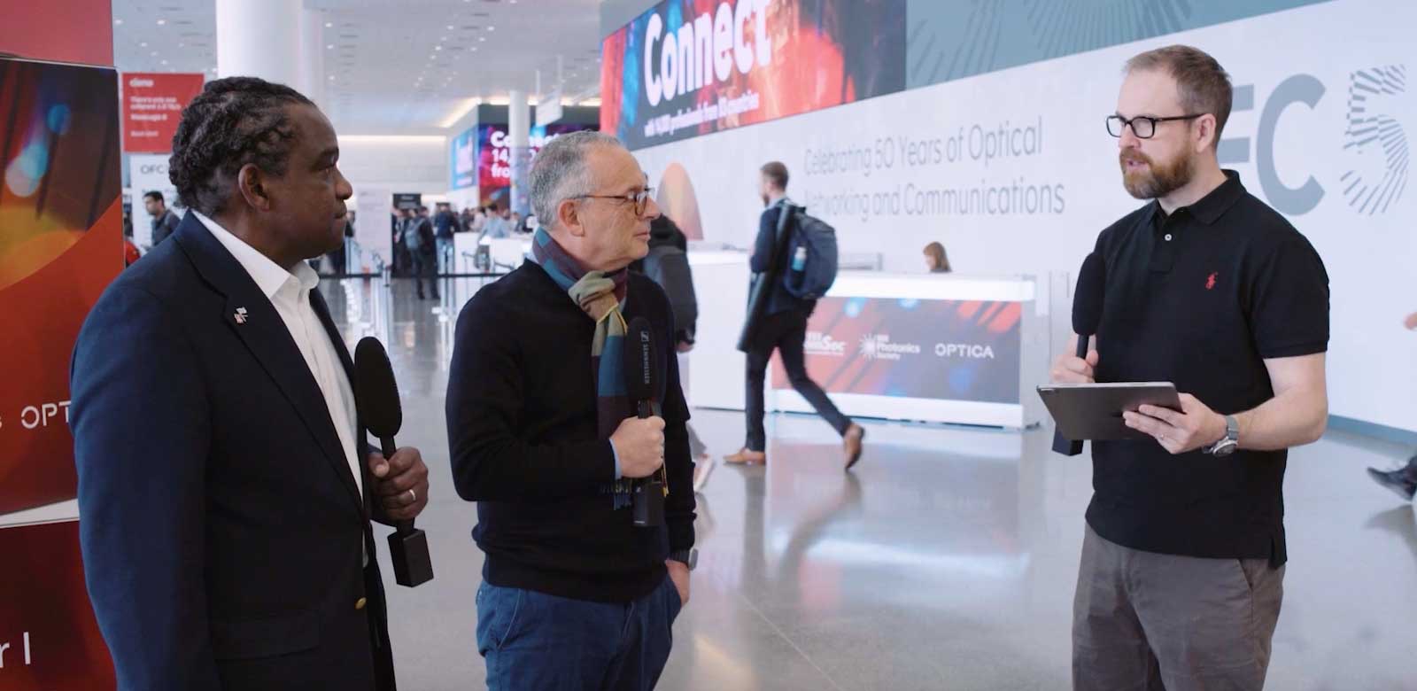
At the OFC 2025 Rump Session, held in San Francisco, three teams were set a weighty challenge. If a catastrophic event—a visit by aliens —caused the destruction of the global telecommunications network, how would each team’s ‘superheroes’ go about designing the replacement network? What technologies would they use? And what issues must be considered?
The Rump Session tackled a provocative thought experiment. If the Earth’s entire communication infrastructure vanished overnight, how would the teams go about rebuilding it?
Twelve experts – eleven from industry and one academic – were split into three teams.
The teams were given ten years to build their vision network. A decade was chosen as it is a pragmatic timescale and would allow the teams to consider using emerging technologies.
The Rump Session had four rounds, greater detail being added after each.
The first round outlined the teams’ high-level visions, followed by a round of architectures. Then a segment detailed technology, the round where the differences in the team’s proposals were most evident. The final round (Round 4), each team gave a closing statement before the audience chose the winning proposal.
The Rump Session mixed deep thinking with levity and was enjoyed by the participants and audience alike.
Round 1: Network vision
The session began with each team highlighting their network replacement vision.
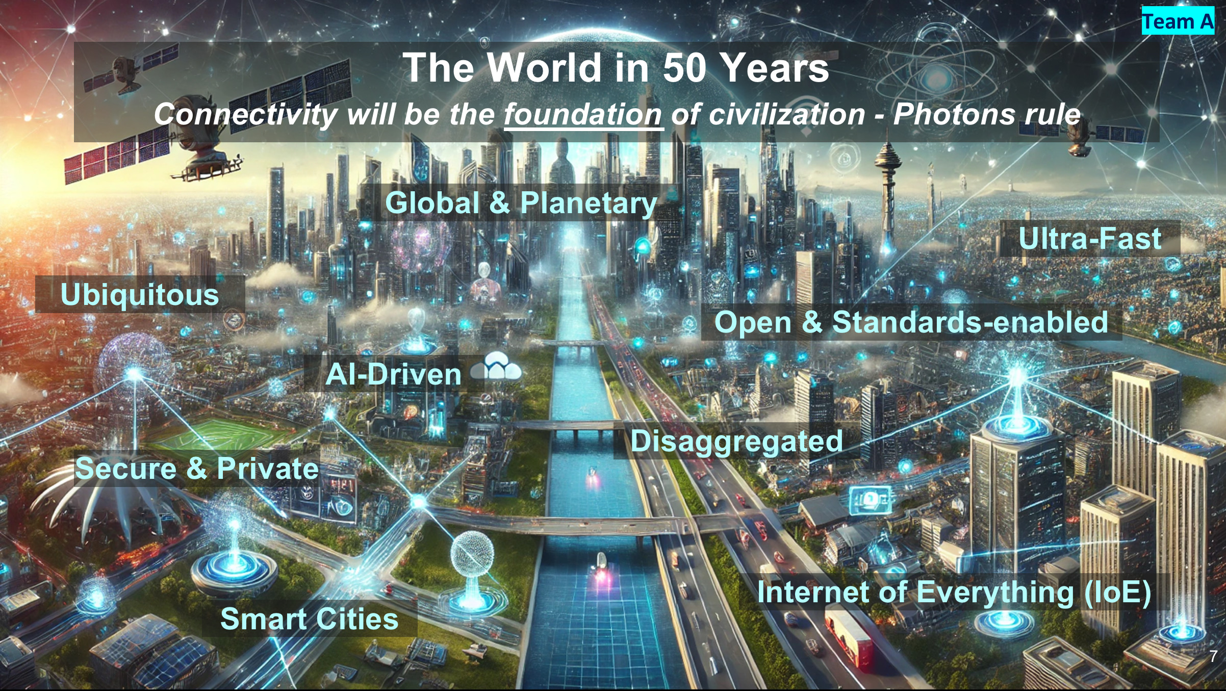
Team A’s Rebecca Schaevitz opened by looking across a hundred-year window. Looking back fifty years to 1975, networking and computing were all electrical, she said, telephone lines, mainframe computing, radio and satellite.
Schaevitz said that by 2075, fifty years hence, connectivity will be the foundation of civilisation. The key difference between the networks a century apart is the marked transition from electrons to photons.
In the future vision, everything will be connected—clothes, homes, roads, even human brains—using sensors and added intelligence. As for work, offices will be replaced with real-time interactive holograms (suggesting humanity will still be working in 2075).
Schaevitz then outlined what must be done in the coming decade to enable Team A’s Network 2075 vision.
The network’s backbone must be optical, supporting multiple wavelengths and quantum communications. Team A will complement the fixed infrastructure with terabit-speed wireless and satellite mega-constellations. And AI will enable the network to be self-healing and adaptive, ensuring no downtime.
Vijay Vusirikala outlined Team B’s network assumptions. Any new network will need to support the explosive growth in computing and communications while being energy constrained. “We must reinvent communications from the ground up for maximum energy savings,” said Visurikala.
But scarcity—in this case energy—spurs creativity. The goal is to achieve 1000x more capacity for the same energy demand.
The network will have distributed computing based on mega data centres and edge client computing. Massive bandwidth will be made available to link humans and to link machines. Lastly, just enough standardisation will be used for streamlined networking.
Team C’s Katharine Schmidtke closed the network vision round. The goal is universal and cheap communications, with lots of fibre deployed to achieve this.
The emphasis will be on creating a unified fixed-mobile network to aid quick deployment and a unified fibre-radio spectrum for ample connectivity.
Team C stressed the importance of getting the network up and running by using a modular network node. It also argued for micro data centres to deliver computing close to end users.
Global funding will be needed for the infrastructure rebuild, and unlimited rights of way will be a must. Unconstrained equipment and labour will be used at all layers of the network.
Team C will also define the communication network using one infrastructure standard for interoperability. One audience member questioned the wisdom of a tiny committee alone specifying such a grand global project.
The network will also be sustainable by recycling the heat from data centres for crop production and supporting local communities.
Round 2: Architectures
Team A’s Tad Hofmeister opened Round 2 by saying what must change: the era of copper will end – no copper landlines will be installed. The network will also only use packet switching, no more circuit switch technology. And IPv4 will be retired (to great cheering from the audience).
Team A also proposed a staged deployment. First, a network of airborne balloons will communicate with smartphones and laptops, which will be connected to the ground using free-space optical links.
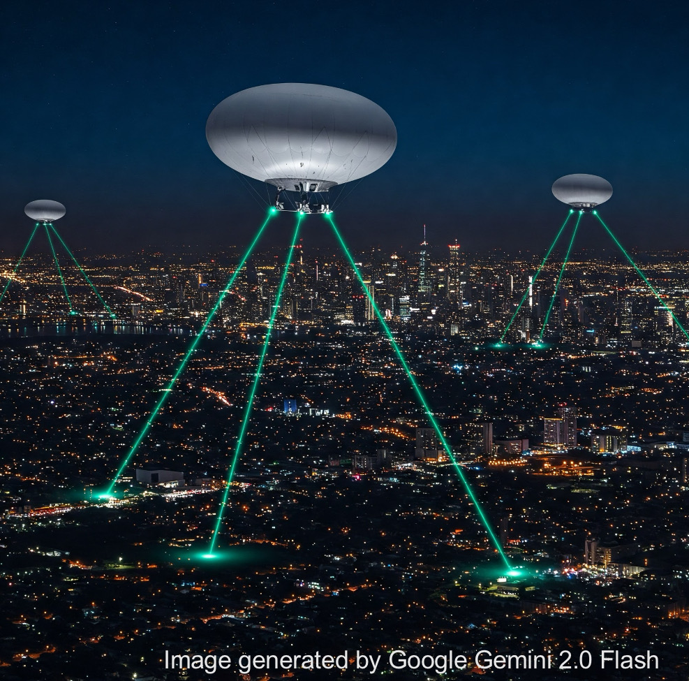
Stage 2 will add base stations complemented with satellite communications. Fibre will be deployed on a massive scale along roads, railways, and public infrastructure.
Hofmeister stressed the idea of the network being open and disaggregated with resiliency and security integral to the design.
There will be no single mega-telecom or hyperscaler; instead, multiple networks and providers will be encouraged. To ensure interoperability, the standards will be universal.
Security will be based on a user’s DNA key. What about twins? asked an audience member. Hofmeister had that covered: time-of-birth data will be included.
Professor Polina Bayvel detailed Team B’s architectural design. Here, packet and circuit switching is proposed to minimise energy/bit/ km. It will be a network with super high bandwidths, including spokes of capacity extending from massive data centres connecting population centres.

Bayvel argued the case for underwater data centres: 15 per cent of the population live near the coast, she said, and an upside would be that people could work from the beach.
Team C’s Glenn Wellbrock proposed unleashing as much bandwidth as possible by freeing up the radio spectrum and laying hollow-core fibre to offer as much capacity as possible.
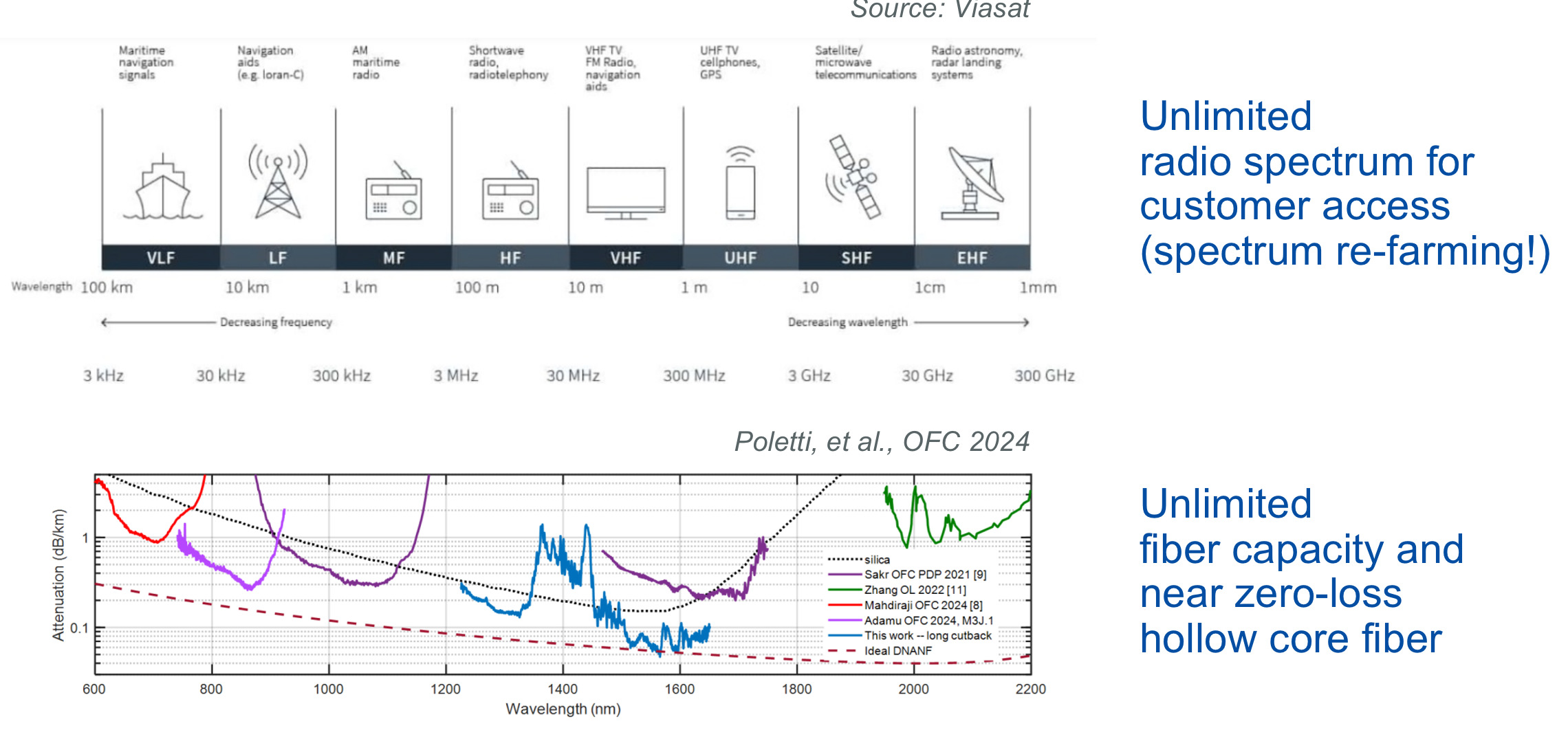
Wellbrock views hollow-core fibre as a key optical communications technology that promises years of development, just like first erbium-doped fibre amplifiers (EDFAs) and then coherent optics technology have done.
Team C showed a hierarchical networking diagram mapped onto the geography of the US – similar to today’s network – with 10s of nodes for the wide area network, 100s of metropolitan networks, and 10,000s of access nodes.
Wellbrock proposes self-container edge nodes based on standardised hardware to deliver high-speed wireless (using the freed-up radio spectrum) and fibre access. There would also be shared communal hardware, though service providers could add their own infrastructure. Differentiation would be based on services.
AI would provide the brains for network operations, with expert staff providing the initial training.
Round 3: Technologies
Round 3, the enabling technologies for the new network, revealed the teams’ deeper thinking.
Team A’s Chris Doerr advocated streamlining and pragmatism to ensure rapid deployment. Silicon photonics will make a quick, massive-scale, and economic deployment of optics possible. Doerr also favours massive parallelism based on 200 gigabaud on-off keying (not PAM-4 signalling). With co-packaged optics added to chips, such parallel optical input-output and symbol rate will save significant power.
Standards for all aspects of networking will be designed first. Direct detection will be used inside the data centre; coherent digital signal processing will be used everywhere else. More radically, in the first five years, all generated intellectual property regarding series, converters, modems, and switch silicon will be made available to all competition. Chips will be assembled using chiplets.
For line systems, C-band only followed by the deployment of Vibranium-doped optical amplifiers (Grok 3 gives a convincing list of the hypothetical benefits of VDFAs). Parallelism will also play a role here, with spatial division multiplexing preferred to combining a fibre’s O, S, C and L bands.
Like Team C, Doerr also wants vast amounts of hollow-core fibre. It may cost more, but the benefits will be long-term, he said.
Peter Winzer (Team B) also argued for parallelism and a rethink in optics: the best ‘optical’ network may not be ‘optical’ given that photons get more expensive the higher the carrier frequency. So, inside the data centre, using the terahertz band and guided-wave wire promises 100x energy per bit benefits compared to using O-band or C-band optics.
Winzer also argues for 1000x more energy-efficient backbone connectivity by moving to 10-micron wavelengths and ultra-wideband operation to compensate for the 10x spectral efficiency loss that results. But for this to work, lots of fibre will be needed. Here, hollow-core fibre is a possible option.
Chris Cole brought the round to a close with radical ways to get the networking deployed. He mentioned Meta’s Bombyx, an installation machine that spins compact fibre cables along power lines.
Underground cabling would use nuclear fibre boring (including the patent number) which produces so much heat that it bores a tunnel while lining its walls with the molten material it produces. An egg-shaped portable nuclear reactor to power data centre containers was also proposed.
Cole defined a ‘universal’ transceiver with quadruple phase-shift keying (QPSK) modulation with no digital signal processing. “Spectral efficiency is not important as fibre will be plentiful,” says Cole.
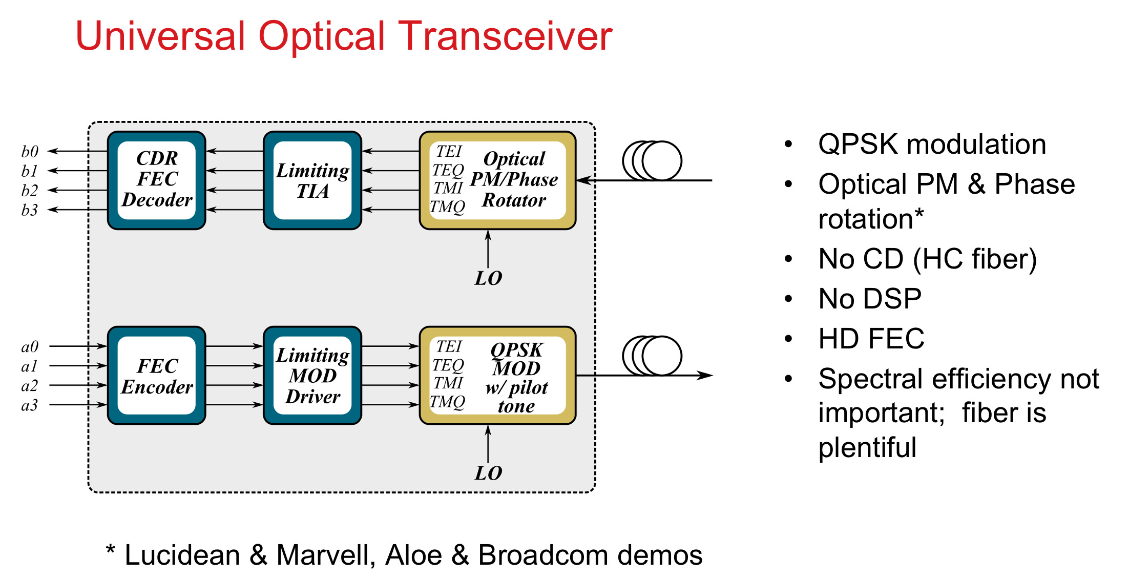
Completing arguments
After each team had spent a total of some 14 minutes outlining their networks, they were given one more round for final statements.
Maxim Kuschnerov expanded on the team’s first-round slide, which outlined the ingredients needed to enable its Network 2075 vision. He also argued that every network element and connected device should be part of a global AI network. And AI will help co-design the new access network.
The new network will enable a massive wave of intelligent devices. Data will be kept at the edge, and the network will enable low-latency communications and inferencing at the edge.
Team B’s Dave Welch outlined some key statements: fusion energy will power the data centres with 80 per cent of the energy recycled from the heat. Transistors will pass the 10THz barrier, there will be 1000x scaling for the same energy, and an era of atto-joules/bit will begin. “And human-to-human interactions will still make the world go round,” says Welch.
Team C’s Jörg-Peter Elbers ended the evening presentations by outlining schemes to enable the new network: high-altitude platforms in a mega constellation (20km up) trailing fibre to the ground.
Such fibres and free-space links would also act as a sensing early-warning system in case the aliens returned.

Lastly, Elbers suggested we all get a towel (an important multi-purpose tool as outlined in Douglas Adams’ The Hitchhiker’s Guide to the Galaxy). A towel can be used for hand-to-hand combat (when wet), ward off noxious fumes, and help avoid the gaze of the Ravenous Bugblatter beast of Traal. Lastly, and in the spirit of the evening, if all else fails, a towel can be used for sending line-of-sight, low-bandwidth smoke signals.
Team C ended the presentations by throwing towels into the audience, like tennis stars after a match.

Common threads
All the teams agreed that fibre was necessary for the network backbone, with hollow-core fibre widely touted.
Two of the teams emphasised a staged rollout and all outlined ways to avoid the ills of existing legacy networks.
Differences included using satellites rather than fibre-fed high-altitude balloons, which are quicker and cheaper to deploy, and the idea of container edges rather than a more centralised service edge. All the teams were creative with their technological approaches.
What wasn’t discussed – it wasn’t in the remit – was the impact of a global disconnect on the world’s population. We would suddenly become broadband have-nots for several years, disconnected from smartphones and hours-per-day screen time.
The teams’ logical assumption was to get the network up and running with even greater bandwidth in the future. But would gaining online access after years offline change our habits? Would we be much more precious in using our upload and download bits? And what impact would a global comms disconnect have on society? Would we become more sociable? Would letter-writing become popular again? And would local communities be strengthened?
Maxim Kuschnerov came closest to this when, in his summary talk, he spoke about how the following iteration of network and communications should be designed to be a force for good for humanity and for its economic prospects.
Team winners
The audience chose Team B’s network proposal. However, the choice was controversial.
An online voting scheme, which would have allowed users to vote and change their vote as the session progressed, worked perfectly, but keeled over on the night.
The organisers’ fallback plan, measuring the decibel level of the audience’s cheers for each team, ended in controversy.
First, not all the Session attendees were present at the end. Second, a couple of the participants were seen self-cheering into a microphone. Evidence, if needed, as to the seriousness the ‘superheroes’ embraced architecting a new global network.
“It has been an evening of pure creative chaos: the more time I spend reflecting on the generated ideas, the more their value increases to me,” says Antonio Tartaglia of Ericsson, one of the organisers. “The voting chaos has been an act of God, because all three teams deserved to win.”
Tartaglia came up with this year’s theme for the Rump Session.
“Rump sessions are all about creative debate, and this year’s event took that to its full potential,” says Dirk van den Borne of Juniper Networks, another of the organisers. “Micro data centres, fibre-tethered balloons, Terahertz waveguides, and communication by pigeon; the sheer breath of ideas shows what an exciting and inventive industry we’re working in.”
The evening ended with a tribute to Team C’s Glenn Wellbrock. BT’s Professor Andrew Lord acknowledged Wellbrock’s career and contribution to optical communications.
Wellbrock officially retired days before the Rump Session.
oDAC: Boosting data centre speeds with less power

Academics have developed an optical digital-to-analogue converter (oDAC) that promises to rethink how high-speed optical transmission is done.
Conceived under the European Commission-funded Flex-Scale project for 6G front-haul, the oDAC also promises terabit links inside the data centre.
The oDAC is expected to deliver a 40 per cent power savings for a 1.6 terabit optical transmitter, the ‘send’ path of an optical module.
“It might not be not 50 or 60 per cent, but in this field, even a 25 per cent power saving turns heads,” says Ioannis Tomkos, a professor at the Department of Electrical and Computer Engineering at the University of Patras, Greece, one of the researchers leading the work.
The first proof-of-concept oDAC photonic integrated circuit (PIC) has sent 250 gigabits per second (Gbps) over a single wavelength as part of the European Proteus programme.
The goal is to bring the oDAC to market in 2026.
High-speed optical transmission challenges
An optical interface acts as a gateway between the electrical and optical domains.
The main two classes of optical interfaces—pluggable modules for the data centre and coherent designs for longer-distance links—continue to grow in data rate.
The upcoming rate today is 1.6 terabits per second (Tbps), with 3.2Tbps optical links are in development. But going faster adds design complexity and consumes extra power.
Faster electrical signalling must use encoding schemes such as 4-level pulse amplitude modulation (PAM-4). And in the optical domain, PAM-4 is used in the data centre while higher-order modulation schemes such as 16-ary quadrature amplitude modulation (16-QAM) are used for long-haul optical transmissions. Quadrature amplitude modulation uses amplitude and phase modulation thyat doubles transmission capacity.
Such schemes require fast analogue-to-digital converters (ADCs), digital-to-analogue converters (DACs), and digital signal processing (DSPs) to compensate for transmission impairments. But as speeds increase, so does the signalling complexity and sampling rates, driving up the overall cost and power consumption.
The trends are leading researchers to consider alternative approaches, such as signal processing in the optical domain, to lessen the demands placed on the DSP and its DACs and ADCs. Researchers are even wondering if such an approach could remove the DSP altogether.
“Step by step,” cautions Tomkos.
Tomkos is working with Professor Moshe Nazarathy, a founder of the oDAC work, at the Faculty of Electrical Engineering at Technion University, Israel.
And it is developing the oDAC where they have first focussed their efforts.
Electronic DAC versus the oDAC
One way to view the oDAC is as a high-speed optical modulator. Another is as a multiplexer of multiple optical amplitude data streams.
The oDAC is a fundamental building block that trades extra optical components to simplify the electrical drivers for the high-speed transmitter. This is how the 40 per cent power saving is achieved.
The oDAC’s architecture is similar to that of a coherent optical transmitter but with notable differences.

In a coherent optical transmitter setup, the laser source is split evenly to feed the in-phase and quadrature Mach-Zehnder modulators (MZMs), with a 90-degree phase shifter in one of the modulator’s arms (see diagram above, left).
In contrast, the oDAC employs a variable splitter and a combiner at the input and output stages, paired with identical Mach-Zehnder modulators (no phase shifter is used in one of the modulator’s arms, see diagram, right). The ODACs can be used in a nested arrangement, as part of in-phase and quadrature arms, for coherent optical transmission.
Conventional electronic DACs (eDACs in the diagram) sample the data at least as high as the symbol rate and have a finite bit resolution, which limits the higher-order modulation schemes that can be used.
They are used to drive the optical Mach-Zehnder modulator, which has a non-linear sine-shaped response. The non-linearity forces the modulator to work only in the linear region of its transfer function. (See graph below.)

This curtailing of the driver saves power but results in ‘modulator loss’ – the full potential of the modulator is not being used, impacting signal recovery at the optical receiver.
In contrast, the oDAC can drive fully the modulator, thereby avoiding the modulator backoff loss.
Another key oDAC benefit is that each of its Mach-Zehnder modulators is driven using simpler PAM driver chips to produce higher-order PAM signals: two standard PAM-4 drivers can produce PAM-16 and using two oDAC PAM-16s can be used to generate PAM-256 (each symbol carrying 4- or 8-bits, respectively).
No commercial electronic PAM-16 drivers exist, says Tomkos.
Scaling data rates using PAM-4 drivers
A PAM-4 driver for the oDAC’s Mach-Zehnder modulator arm produces a four-level “staircase” waveform. Adjusting the oDAC’s splitter ratio to 4:1 and summing the outputs yields 16 distinct levels (diagram, below)

n effect, two simple signals can be stacked in multiple combinations to mimic a complex one. For PAM-16, one Mach-Zehnder modulator handles levels 0, 1, 2, and 3, while the other one, scaled differently (e.g., 0, 4, 8, 12), ensures a sum from 0 to 15.
The catch? Achieving a smooth staircase signal requires precise in-phase combining and level controls so there are no differences between the two Mach-Zehnder arms, which requires careful circuit control.
“Every programmable photonic circuit in general, for whatever application, needs some parametric control of the actual circuit,” says Tomkos. “For our case, it is so that it will not deviate if you change the temperature if you have vibrations or any other environmental changes.”

David Moor, a post-doctorate researcher at ETH-Zürich, part of the Flex-Scale project, and the director of photonic IC design at Emitera, the start-up tasked with bringing the oDAC to market, has been putting the prototype oDAC photonic integrated circuit through lab tests.
To send 500 Gbps over a single wavelength, a two-arm oDAC is used, with each PAM4-driven arm operating at 120 gigabaud symbol rate, or 250Gbps. While using two oDACs feeding an in-phase and quadrature coherent structure, doubles the data rate to 1Tbps.
Then, using a pair of PAM-16 oDACs (each driven by a pair of PAM-4 signals, in-phase and quadrature-combined in a coherent transmitter structure, further doubles the data rate to 1.6Tbps.

Transmissions at 3.2 terabits would need the symbol rate at 240 GBd.
What next?
Professor Nazarathy, working with Professor Birbas and his team at the University of Patras, are developing an FPGA-based control system to ensure the device operates optimally in real-world conditions.
“In the lab, the device has been quite stable,” says Moor. But any environmental changes throw it off track. oDAC device needs robust control to be a commercial product.
A second-generation oDAC photonic integrated circuit design and an FPGA-based control system are in the works and are expected to be up and running in six months.
Applications: Data centres and front-haul
“The higher-order the modulation format used, from 16-QAM to 256-QAM, the less the distance,” says Tomkos. “This is a law of information theory. You cannot do otherwise; nobody can.”
But the benefit of the design grows the higher the modulation order and the higher bit rate. Thus, the oDAC comes into its own when using 16-QAM and higher-order signalling schemes.
Accordingly, the ODAC’s sweet spot is for links up to 20 or even 40km, where terabits of data can be pushed over an optical wavelength. This makes the oDAC concept ideal for “coherent-lite” spans between campuses and when used inside the data centre.