

Adtran breaks the 1W barrier with 800G linear pluggable optics
-
Adtran has developed a 0.8W 800-gigabit DR8 module.
-
Using single-mode VCSELs rather than electro-absorption modulate lasers (EMLs) or silicon photonics modulators is central to achieving the low power.
Adtran has announced an 800-gigabit linear pluggable optics (LPO) transceiver designed for short-reach data centre links.
The LiteWave800 is an OSFP 800G-DR8 module with a reach of 500 metres that consumes less than 1 watt of power, enabled by the use of 100-gigabit single-mode VCSEL lasers.
“We have partners that we have been working with on single-mode VCSELs, and the devices are going to be part of our LPO platform that we’re announcing at [the upcoming] OFC [show],” says Saeid Aramideh, Vice President of Business Development, Optical Engines business unit at Adtran.
AI workloads and the push for LPO
“AI workloads are driving everything, and these require much higher interconnect bandwidth than what we are typically used to seeing,” says Aramideh.
Not only are AI clusters driving the need for higher interconnect speeds, but the designs are also raising issues of link reliability, latency, system cost, and energy efficiency.
“Power consumption has become the most critical limiting factor in large-scale data centres, and is directly impacting rack density: how many pluggables you can put in there, cooling requirements and so on,” says Aramideh. “Ultimately, the issue of power is going to impact the economic viability of the infrastructure.”
The attraction of LPO is that it uses an optimised electrical-optical interface with the host IC driving the optical link. The approach eliminates the need for the pluggable module to have its own digital signal processor (DSP), a key contributer to the overall power consumption.
First-generation LPO modules consume between 5–8W, compared with well over 10W for conventional DSP-based 800-gigabit pluggables, says Aramideh.
Adtran set itself an energy consumption target of 1pJ/b for its LiteWave800 design. At 800 gigabits-per-second (Gbps), an energy efficiency of 1pJ/b corresponds to roughly 0.8W total module power, significantly lower than conventional DSP-based modules.
Design approach
To achieve the ambitious power target, Adtran used its in-house electronics IC design team, along with using single-mode VCSEL technology operating in the 1310nm band for the optics.
“The choice of single-mode VCSELs in the module is the most essential defining factor when it comes to reducing the power,” says Aramideh. Using EML lasers or a silicon photonics modulator approach yields much higher energy numbers, ranging from 5-15pJ/b.
Multi-mode VCSELs are an established industry technology. Developing single-mode VCSELs is challenging, as is creating a supply of such devices. But the laser device has advantages such as its low drive voltage and good linear performance.
Adtran has also been using single-mode VCSELs for its 10×10 gigabit MicroMux pluggable product and says it has two supply partners for its VCSELs.
Adtran also decided to make its own electronics as typical driver and trans-impedance amplifiers in the pluggable consume up to 3pJ/b.
“But low power is essentially meaningless if you cannot have good signal integrity,” says Aramideh. Given that signal integrity is the biggest challenge with an LPO design, Adtran’s focus was on how to close the loop between the optics and the host driver IC.
Making use of the OIF’s Common Management Interface Specification, or CMIS, Adtran created a set of controls known as the Versatile Control Set (VCS).
“VCS lets you manage certain attributes on the host DSP, and these attributes set the operating margin and tune parameters to coordinate the signal integrity between the module and the host, and control them dynamically,” says Aramideh.
LiteWave800 architecture
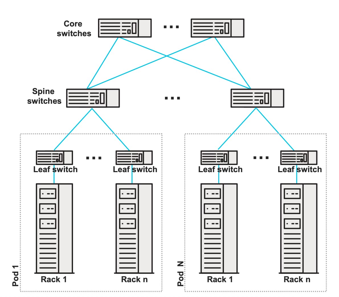
The 800-gigabit module has eight 100-gigabit channels, each operating at a 53-gigabaud symbol rate and the PAM4 modulation format.
The drivers interface to the VCSELs which also use a thermal-electric cooler. However, based on testing results, such coolers may be optional depending on the pluggables’ environmental conditions. On the receive side of the pluggable, there are photodiodes and two quad trans-impedance amplifiers (TIA).
The expertise Adtran brings is in controlling the single-mode VCSEL, interfacing the drivers and the VCSELs, and the overall link control.
Roadmap beyond 100 gigabit-per-lane
One question facing the industry is whether LPO architectures can scale to 200 gigabits-per-lane, where tighter electrical margins may require alternative approaches. Is Adtran’s LiteWave design thus a one-generation product?
“There is a roadmap, but it may not necessarily be LPO,” says Aramideh. He cites the use of near-packaged optics for next-generation AI clusters, where the optics are brought closer to the host IC.
Using near-packaged optics based on single-mode VCSELs and linear electronics and addressing the challenges of serviceability and thermal coupling might prove a better approach, argues Aramideh.
“Can we get to 200 gigabit per lane? The answer is absolutely, and we must. This is what industry is asking for,” says Aramideh. “Would the answer be an LPO? At this point, that is a question mark and maybe near packaged optics would prove a better solution.”
Market implications
Aramideh hopes there will be an uptake of single-mode VCSELs, leading to wider adoption of the technology in the data centre.
He also believes that the LiteWave800 design benefits pluggables overall by offering an attractive alternative to the low-power argument used by co-packaged optics proponents. Such designs typically consumes 5pJ/b.
“Having a product at 800 gigabit that hits one picojoules per bit, that sets the industry standard,” says Aramideh.
The product will be available as samples in the third quarter of this year and will be in production early 2027.


Credo’s 224G Blue Heron retimer targets AI Scale-Up
Credo has unveiled its Blue Heron retimer chip, designed for line cards used in AI servers.
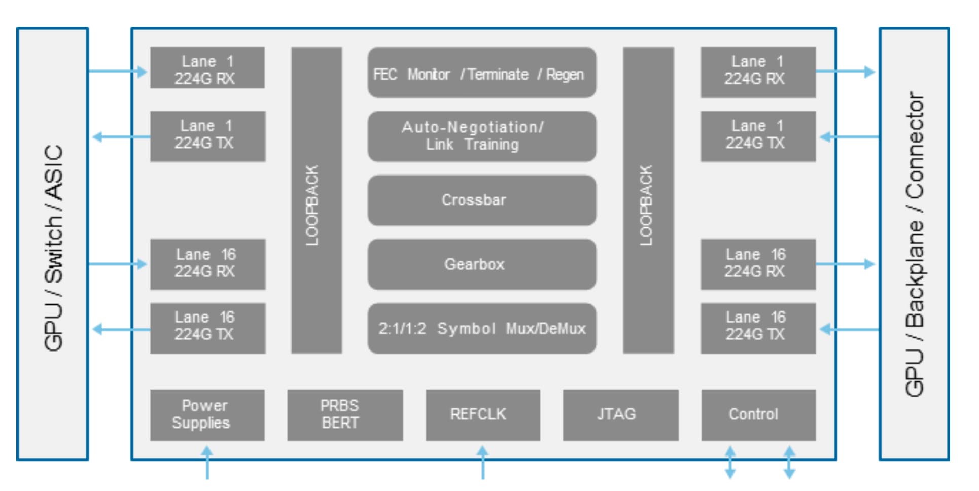
Blue Heron uses 224-gigabit serialiser-deserialisers (SerDes) for a total capacity of 3.2 terabits: 16 lanes in and 16 lanes out.
Credo has long supplied line-card retimer chips, at 56-gigabit, 112-gigabit, and now at 224-gigabit line rates. Such retimers are already used for scale-out networking.
What excites Credo is AI scale-up: the opportunity to keep growing the number of AI accelerator chips such that processing performance scales linearly.
This requires high-bandwidth links and the ability to use copper across long links.
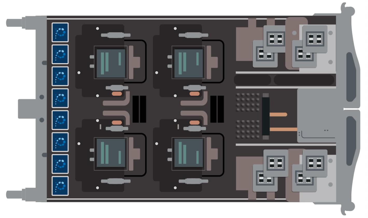
“We’re positioning the Blue Heron line card device for scale-up networking,” says Sandeep Shah, Assistant Vice President for Credo’s Retimer Products. “As scale-up moves from proprietary to using an Ethernet PHY (physical layer device), it’s a huge opportunity for us.”
To this end, Blue Heron’s physical layer supports key emerging scale-up protocols, such as UALink, ESUN, and Ethernet.
Supporting multiple protocols ensures the retimer aligns with broader data centre ecosystems while avoiding overcommitment to proprietary interconnect schemes.
Revenue growth
Credo has achieved significant revenue growth in the last two years.
Revenues were up 226% year-on-year to $437 million in fiscal year 2025 (ending April ‘25), while for fiscal year 2026, revenues are expected to more than double again (up 251%) to $1.19 billion.
The company’s growth can be directly attributed to the networking needs of AI racks used by the hyperscalers, in large part due to its active electrical cable portfolio. Its retimer ICs have long been used in data centre switches and router platforms. Now Credo is eyeing the AI scale-up opportunity.
From 112G to 224G: A Nonlinear Challenge
Doubling the speed from 112 gigabit-per-second (Gbps) to 224Gbps with a SerDes IC while maintaining existing reaches is a considerable engineering undertaking.
On paper, electrical reach roughly halves when lane speed doubles. In practice, careful retimer design can claw back some distance.
Power per bit also rises from 112 gigabit to 224 gigabit, though engineering efforts aim to optimise efficiency at the bit level.
The trade-off is clear: higher performance and extended reach come at the cost of increased complexity and silicon investment.
Why 3nm CMOS
Credo has long marketed an “N minus one” philosophy—delivering competitive power and signal performance using an older CMOS process node than competitors. If similar performance can be achieved using a more mature CMOS node, cost and supply advantages follow.
Credo says the pattern no longer applies at 224 gigabit. Credo’s Blue Heron uses a 3nm CMOS process due to the complexity of the digital signal processing.
For 224-gigabit 4-level pulse-amplitude modulation (PAM4) signalling, the transmitter and receiver requirements scale nonlinearly. Channel loss budgets around 40dB become significantly harder to close, given that receiver equalisation demands are higher.
Earlier 112-gigabit designs used 21 receiver filter taps. Credo has increased the number of taps substantially to 30 for fast-forward equalisation, compensating for signal distortion introduced by the channel at 224 gigabit. An extra 16 taps are also used to manage reflections, noise, and inter-symbol interference. Equalisation must be more precise and adaptive at 224 gigabit, which makes it more computationally intensive.
Link training to establish a stable link takes about 10 seconds, during which the device characterises the channel and configures the equaliser. But after the link-up stage, adaptation continues. Temperature changes, for example, can subtly alter channel characteristics, and the retimer compensates to prevent rising bit-error rates and the risk of burst errors.
Firmware running on an embedded microcontroller inside the device orchestrates these calibration and adaptation routines.
The 224-gigabit Blue Heron line card retimer’s 16 lanes in and 16 lanes out is common across retimer generations. With 16, 224-gigabit SerDes, a Blue Heron chip supports flexible configurations: two 1.6-terabit ports, four 800-gigabit ports, or other combinations.
Looking towards 448 gigabit links
The next step—448-gigabit SerDes—will test copper’s limits, standardisation work that the OIF has already started.
Whether copper can stretch meaningfully beyond inside-rack distances at 448 gigabit remains an open question.
For now, 224 gigabit represents a balancing act. Reach drops modestly, digital signal processing complexity rises sharply, and silicon has to move to a leading-edge node. But AI system densification may give copper more room than previously assumed.
Inside compact GPU clusters, the economics of copper—augmented by increasingly sophisticated retimers—works, claims Credo.
Copper’s advancement may require ever more engineering effort and advanced CMOS but it is not retreating quietly.

GlobalFoundries’ silicon photonics push after AMF acquisition
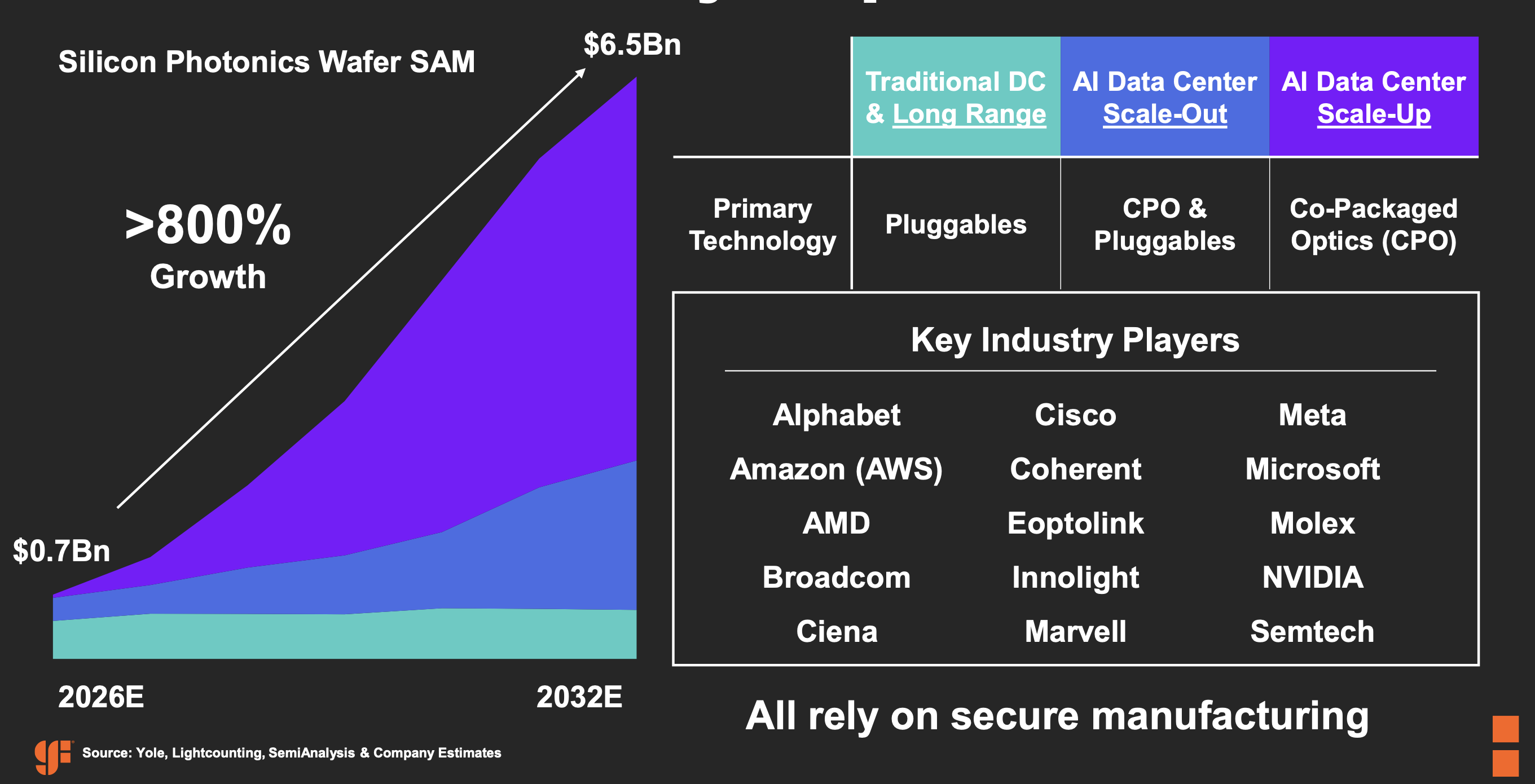
Silicon photonics has reached an inflexion point, says Kevin Soukup, senior vice president at GlobalFoundries’ silicon photonics business, who points out that the foundry is fielding new enquiries.
“We see customers that don’t have an optics strategy coming to GlobalFoundries now,” says Kevin Soukup. “Even if they don’t have a photonics design team, they want to engage to build out their optical strategy.”
The shift marks a decisive change from a year ago, when the industry was still debating the scale of silicon photonics’ adoption. That debate, says Soukup, has been settled by a wave of co-packaged optics announcements and an insatiable demand for bandwidth driven by AI data centre build-outs.
And GlobalFoundries has recently acquired Advanced Micro Foundry (AMF). The deal places GlobalFoundries at the top in terms of silicon photonics revenue, but it will certainly re-energise the competition, said LightCounting Market Research in a research note published last November.
AMF acquisition
Buying Singapore-based AMF is central to GlobalFoundries’ ambitions. “AMF brings a whole set of different customers,” says Soukup. One of AMF’s strengths lies in coherent optics for long-haul applications, which Soukup says exceeds what GlobalFoundries had achieved independently.
AMF’s team has built a successful business, supporting more than 300 customers, mostly in Asia, developing silicon photonics products across a range of applications, including optical communications, says LightCounting.
AMF has also been working to bring in optical modulator materials and to integrate indium phosphide laser chips onto silicon – critical technologies for staying ahead of the competition. For example, for 400 gigabit technology, AMF has been using thin-film lithium niobate and polymer-based modulator approaches.
The combined R&D teams, bolstered by A*STAR’s broader resources in Singapore, are now focused on a unified roadmap spanning pluggables, co-packaged optics, and emerging markets, including quantum computing, LIDAR, and automotive connectivity.
There is also another dimension to the deal. AMF operated on a government research site with limited room to expand, which constrained its ability to win customers that required volume production. “There are a lot of customers that liked AMF’s technology but never saw a path to scale,” says Soukup.
GlobalFoundries’ own campus in Singapore, with its large-scale 200mm and 300mm wafer capacity, removes that constraint. The plan is to offer AMF’s customers a transition path into a high-volume manufacturing environment.
Meeting market needs
For pluggable transceivers, activity is intense, says Soukup, as transceiver companies develop higher-speed devices.
“We see quite a bit of adoption in the scale-out section of the market, so many different pluggable transceiver companies coming looking for not just 200 gigabit-per-lane products, which are in qualification stage now, but 400 gigabit per lane,” he says. A 200-gigabit-per-lane solution enables 1.6 terabit-per-second (Tbps) pluggables using eight lanes.
Interest extends to 400 gigabit-per-second (Gbps) and 800Gbps coherent single-wavelength pluggable solutions, with the 800ZR+ emerging as a focal point for extended-reach applications. “That’s the direction that we see: ZR+,” says Soukup.
The coherent long-haul market is also evolving. Once confined to telecom networks, coherent optics are now being deployed for ‘scale-across’ networking applications, sharing large AI workloads across data centres.
Evolving role
For pluggables, a high-bandwidth optical modulator capable of supporting 200 gigabits per lane is the entry point. For co-packaged optics, requirements go further: through-silicon vias (TSVs) that support an electronic IC stacked on the photonic IC, with high-density pitch for both power and to ensure signal integrity.
“Many of the electronic IC companies are seeking more digital scaling, and so the ability to support, for example, a 3nm EIC with a high-density pitch of TSVs — that advanced packaging roadmap is really important,” says Soukup.
Fibre attach is also critical. GlobalFoundries is developing a broadband detachable fibre approach that supports multiple wavelengths, an essential capability as the industry moves beyond single-wavelength architectures toward four-lambda and eventually sixteen-lambda designs.
“That allows the technology to scale beyond single wavelength, and we expect bandwidth to rise exponentially,” says Soukup.
He is candid about the state of play: the fibre-attach landscape remains fragmented, with vendors pursuing different approaches—current solutions based on edge coupling work for one or two wavelengths but won’t scale to sixteen.
“Over the next five-plus years, fibre attach is going to change a lot before we reach a standard solution that works for everyone, and we may never get there,” he says.
Monolithic heritage
GlobalFoundries’ heritage in silicon photonics is rooted in monolithic integration—the ability to combine CMOS, radio-frequency circuitry, and silicon photonics on a single chip.
The approach works for certain customers, including those that address LIDAR and pluggable transceivers. GlobalFoundries also offers embedding heater-control circuitry directly on-chip to manage thermal effects that can affect optical performance.
But the foundry recognises its limits. “For some applications, they need more digital horsepower than the monolithic integration supports,” says Soukup, i.e. advanced CMOS process nodes.
GlobalFoundries now supports this with a photonics-only flow alongside its monolithic option: a simpler process with fewer mask steps and lower cycle time, yet one that supports the full advanced packaging stack, including electronic IC stacking and cavity-based fibre attach.
Customers can bring an advanced node electronic IC from another CMOS foundry and co-package it with a GlobalFoundries PIC. The company also has a customer fabricating an electronic IC on its own 22FDX platform.
Modulators
The question of new modulator materials — thin-film lithium niobate, barium titanate, advanced polymers — looms large over the industry’s roadmap for higher baud rates.
Soukup describes the modulator work as pathfinding. The challenge is twofold: can the supply chain scale, and can the new material be encapsulated and integrated without destabilising existing processes?
Development work happens off-site, with coupons and, eventually, full wafers brought in for bonding to GlobalFoundries silicon. “That’s part of the development — can you encapsulate it properly, and can you industrialise that solution? It’s an open question,” he says.
Customisation versus standardisation
A decade of work with universities, consortia, and start-ups generated a wealth of process variants, but at some point, GlobalFoundries had to narrow its focus and industrialise. “There was a time when we started to turn away customers who required customisation,” says Soukup.
That phase is now largely behind the company. The aperture is widening again, though the nature of the customisation has changed: it is more about specific device tweaks and implant set-ups than wholesale process re-architecture. Even so, Soukup notes every customer who downloads the process development kit (PDK) typically asks for something special. “They all have some special sauce that they want.”
Soukup also draws an analogy with the CMOS world. Just as mature semiconductor nodes at 40nm, 28nm, and even older 130nm processes continue to serve high-volume applications long after leading-edge development has moved on, silicon photonics will develop its own hierarchy of maturity.
Edge-coupled fibre attach will serve certain applications; broadband surface-mount detachable solutions will serve others. Modulator and photodiode technologies will follow a similar trajectory.
“Parts of the market will commoditise,” says Soukup. “They’ll reach a level of maturity. They’ll support applications that don’t need that innovation. And then other parts of the market will continue to drive very aggressively to the next greatest thing.”
Pushing silicon photonics
Is silicon photonics settling down? Far from it, says Soukup.
The technology is undergoing what he characterises as leading-edge development, with fibre attach, modulators, photodiodes, electronic IC architectures, and advanced packaging all in active pathfinding.
The AI data centre build-out is accelerating demand, and co-packaged optics for scale-up interconnects could shift the market into a different gear within a few years.
GlobalFoundries, now the largest pure-play silicon photonics foundry following the AMF deal, is betting that its combination of 300mm wafer manufacturing scale, monolithic and heterogeneous integration options, and an advanced photonics and packaging centre in New York will position it at the centre of what Soukup calls the most interesting period the industry has seen.

Marvell on coherent pluggables: “Demand is way outstripping supply”
Russ Esmacher, Senior Vice President and General Manager of the Data Center Interconnect business at Marvell, talks about 800 gigabit ZR+ coherent pluggable modules, the path to 1600 gigabit coherent, and why the pendulum never stops swinging between the digital signal processor and the optics.

Russ Esmacher (pictured) has spent much of his career at the sharp end of coherent optics.
He worked at Cisco and Nokia before joining Infinera, where he spent 5 years and where he helped with its sale to Nokia.
He then took what he describes as time off. It lasted three days.
Matt Murphy, Chairman and CEO of Marvell, and Sandeep Bharathi, President of the Data Center Group at Marvell, asked him to lead the company’s Data Center Interconnect business.
Two months in, Esmacher is direct about the company’s position: Marvell invented the coherent pluggable space with 100 gigabit, he says, and now leads the market.
AI’s impact on coherent pluggables
The rapid scaling of AI workloads has reshaped the coherent pluggable landscape.
According to Esmacher, the last three calendar quarters of 2025 saw demand for 800-gigabit pluggables – 800ZR+ – accelerate with the new application of ‘scale-across’, using optical networking to share AI workloads between data centres.
Classical data centre interconnect has been about linking data centres up to 120 kilometres apart. Scale-across changes that, in the bandwidth between sites and the reach which can be 100km up to 1,000km.
Hyperscalers, under pressure to reserve power for compute and training, pushed the optical industry to bring 800ZR+ forward by roughly 18 months. “They prefer to use power for computing or training, not transport,” says Esmacher. “And so we really accelerated the timeline.”
The huge demand has created a supply chain challenge; not for Marvell, Esmacher notes, but for others entering the space.
“The demand is way outstripping the supply right now,” he says. “It’s a steep ramp; it’s a great problem to have.”
One coherent DSP, several applications
The 800-gigabit ZR+ coherent pluggable has benefited from what the industry learned from the limitations of extending the OIF’s 400-gigabit 400ZR standard.
At 400 gigabits, extending the reach beyond the original ZR design of 120km proved difficult due to the legacy carrier reconfigurable optical add-drop multiplexer (ROADM) passbands, with their associated accumulated impairments, limited optical performance. And combining PIC-based amplification with a 7-nanometre CMOS digital signal processor (DSP) in a pluggable module made the devices run too hot for practical deployment.
The lesson, says Esmacher, was to invest in advanced CMOS nodes so that higher performance, including the use of probabilistic constellation shaping, could fit within a pluggable’s power envelope.
The result is a DSP that serves two roles: 800ZR+, which a reach of 1,000km to 1,500km, and for 400 gigabit using quadrature phase-shift keying (QPSK) to enable 4,000km spans or more.
The 800ZR+ designs are more difficult to make because the optical performance is much higher — the analogue bandwidth of the components and the associated radio frequency (RF) are higher — due to the doubling of the symbol rate up to 135 gigabaud.
“Essentially, we’re squeezing long-haul technology from five years ago into a 30-watt body,” says Esmacher. “Now, it is deployment time.”
New requirements keep emerging too, such as the need for MACsec encryption. As training data increasingly leaves data centres, sovereignty and security concerns are driving demand for encryption regardless of the coherent pluggable’s reach: 100km or 1,000km.
1600 gigabit coherent outlook: two DSPs, not one
Looking ahead to the OIF’s 1600-gigabit coherent standards, Esmacher says 1600ZR and 1600ZR+ pluggable applications will be released at different times.
The 1600ZR standard is further along and closer to market, driven by hyperscaler demand for the shorter-reach application.
Several large hyperscalers are waiting for it, says Esmacher, who expects ZR to account for the larger share of volume — as much as 65-70 per cent — with ZR+ accounting for the remainder.
Marvell believes that the two 1600-gigabit coherent pluggable applications will require separate DSP designs. ZR must be optimised for power and time-to-market, whereas ZR+ must be optimised for optical performance.
Trying to build a single DSP that serves both introduces compromises. “If you’re going to do ZR, it’s power, power, power,” says Esmacher.
The 1600G ZR+ design is expected to use multiple digital subcarriers — two, according to OIF discussions — which would add power and complexity to the DSP, overkill for the shorter-reach application.
1600 gigabit Coherent Light: multiple choices
The emerging ‘Coherent light’ (1600CL) application for intra-data-centre links also draws Esmacher’s attention.
He acknowledges that a de-featured coherent DSP — what he informally calls “ZR minus” — is one path, but not the only one. Two 800G PAM-4 channels could also serve the same application, depending on cost and power trade-offs.
“If I can get there with lower power and cost using two by 800 PAM-4, I’ll do it,” says Esmacher.
He points to Marvell’s position as the market leader in PAM-4, a capability shared by coherent companies such as Acacia.
The 1600CL standard work at the OIF is important, says Esmacher, but the industry should recognise that there are multiple paths.
Pluggables, line systems, and data centre densification
Esmacher frames the broader market shift as a deceptively simple question: are data centres moving further apart or closer together? The answer is closer together, he says.
At first glance, this is counterintuitive, since scale-across has arisen this way. But overall, there is a densification of data centres, with the pluggable transceivers spectral-efficient enough to do the job previously reserved for embedded coherent transponders. And now the pluggables consume significantly less power.
The implication is that embedded coherent engines, once the default for terrestrial long-haul, are increasingly confined to subsea and the longest routes.
However, because pluggables are less spectrally efficient than high-performance embedded engines, moving the same volume of data between sites requires more line system capacity.
Esmacher sees the densification of open line systems — from single-rail to multi-rail architectures — as the key enabler. “That’s where all the emphasis for the next two years is going to go,” he says.
The largest hyperscale deployers of line systems appear to be moving toward C+L bands, though some may opt for high-density C-bands alone.
DSP, optics, and the path to 3.2T terabit coherent
Esmacher likens coherent innovation to a pendulum swinging between the digital and the analogue domains.
When PIC-based amplification emerged around 2018, the pressure was on the DSP: squeezing algorithms into smaller node CMOS. The optics side — silicon photonics modulators and indium phosphide lasers — could coast on existing platforms.
But at 1.6 terabit, the pendulum has swung toward the optics. Silicon photonics modulators are approaching bandwidth limits, potentially prompting a shift to new materials such as thin-film lithium niobate. That transition brings an entirely new foundry and manufacturing ecosystem, but one that starts not at low volumes but high ones.
“It sounds easy going from silicon photonics to thin film lithium niobate,” says Esmacher. “But it’s a whole new ecosystem.”
For 3.2 terabit coherent, he expects the pendulum to swing back toward the DSP, with pressure on the CMOS process node to fit the DSP within a liquid-cooled, 40-to-50-watt power envelope. That likely means moving to a 1.4-nanometre-or-below CMOS process.
But before 3.2 terabit coherent arrives, Esmacher expects 1.6 terabit coherent to have a long market life — not because of the DSP, but because the optical ecosystem needs time to mature.
“These pendulums swing in coherent between the digital and the analogue,” says Esmacher. “At 1.6T, all the pressure is on the analogue. At 3.2T, I think it swings back to the DSP.”

Mixx Technologies’ vision for inference at scale


Mixx’s management team discusses its vision of reshaping AI infrastructure through silicon-integrated optical interconnects.
-
-
“Mixx, still in stealth mode, is developing an interconnect optimised for AI inferencing (tokens-per-second, latency, and power).
-
The start-up has developed a 25.6 terabit-per-second (Tbps) optical engine (chiplet) to enable large AI clusters.
-
Mixx raised $33 million in Series A funding in late 2025.
-
“When you’re stressed about closing your funding, you get horizontal lines,” Vivek Raghuraman, CEO and co-founder of Mixx Technologies, notes wryly, gesturing to his forehead. “Then, the lines go vertical because now we are focused on execution.”
It is a sentiment that will resonate with many start-up CEOs.
Founded in 2023, the San Jose-based company has set out to tackle the escalating data-movement bottleneck in AI clusters.
“At every layer of the AI, we are integrating photonics,” says Raghuraman. “The fundamental thesis for Mixx is mixing optics and electronics in a way that brings efficiency,” he says.
Interconnect challenge
AI training and inference workloads are increasingly limited not by compute but by data movement. Power-hungry electrical links, retimers, and multi-hop switch fabrics have latency and energy overheads, constraining the cluster’s size.
“The fundamental thesis for Mixx is mixing optics and electronics in a way that brings efficiency”
Mixx has developed its ‘HBxIO’ optical engine, a high-density input/output (I/O) chiplet that can be co-packaged with GPUs, custom AI accelerators and other chips such as network interface card controllers and switch chips.
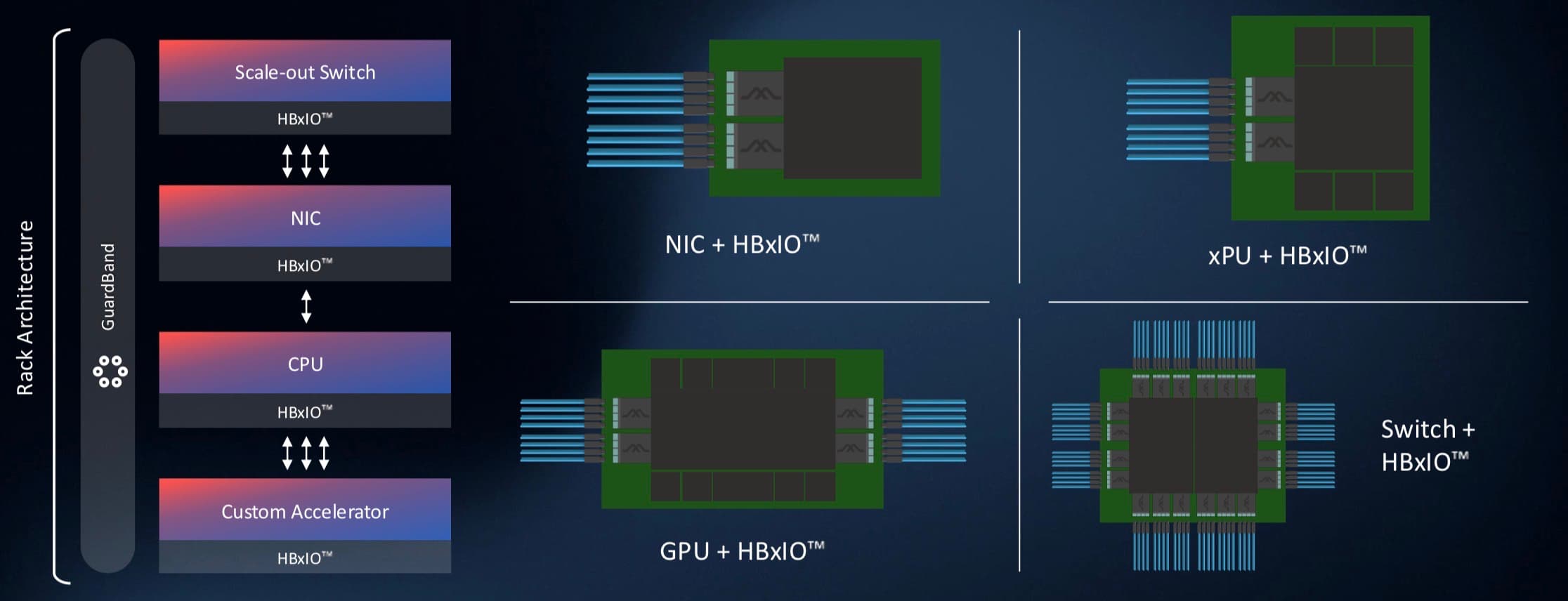
The first-generation HBxIO delivers 25.6 Terabit-per-second (Tbps) of bi-directional bandwidth – 12.8Tbps in each direction – achieved using 200 gigabit-per-second optical lanes.
Bandwidth density is a key metric in advanced packaging where a die’s perimeter edges – its ’beachfront’ – used for I/O are highly valued.
Traditional electrical serial-deserialiser (serdes) interfaces occupy north/south edges of the ASIC, often the shorter edges (some 27mm). In contrast, the ASIC’s east/west beachfronts such as a GPU are used to interface to high-bandwidth memory (HBM).
Mixx’s focus is to achieve high densities by fitting more than 300 fibres across the 27mm die edge. Such density enables a high radix to connect many endpoints without intermediate switches.
“We can bring in more than 300 fibres, connecting at least 128 GPUs,” says Raghuraman, thereby reducing the number of hops between GPUs. “Today, the name of the game is increasing GPUs in a cluster in a way that all can operate as one large processing unit.”
Nvidia’s NVL72 rack, for example, uses 18 switches to connect 72 GPUs in a scale-up architecture. Mixx’s approach enables a switch-less or a minimal-switch cluster for latency-sensitive workloads. Indeed, using both chip edges, 256 GPUs can be connected.
Beyond that, system architects have flexibility: they can add optical or electrical switches for dynamic workloads, or extend to a multi-cluster across 500 meters.
“We’re providing the ability to create a switch-less cluster if latency is the primary goal of the workload,” says Rebecca Schaevitz, co-founder and chief product officer at Mixx. “But if you want dynamic workloads, and can accommodate the extra latency of a switch, you can connect a cluster of more than 4,000 GPUs using one layer of switches.”
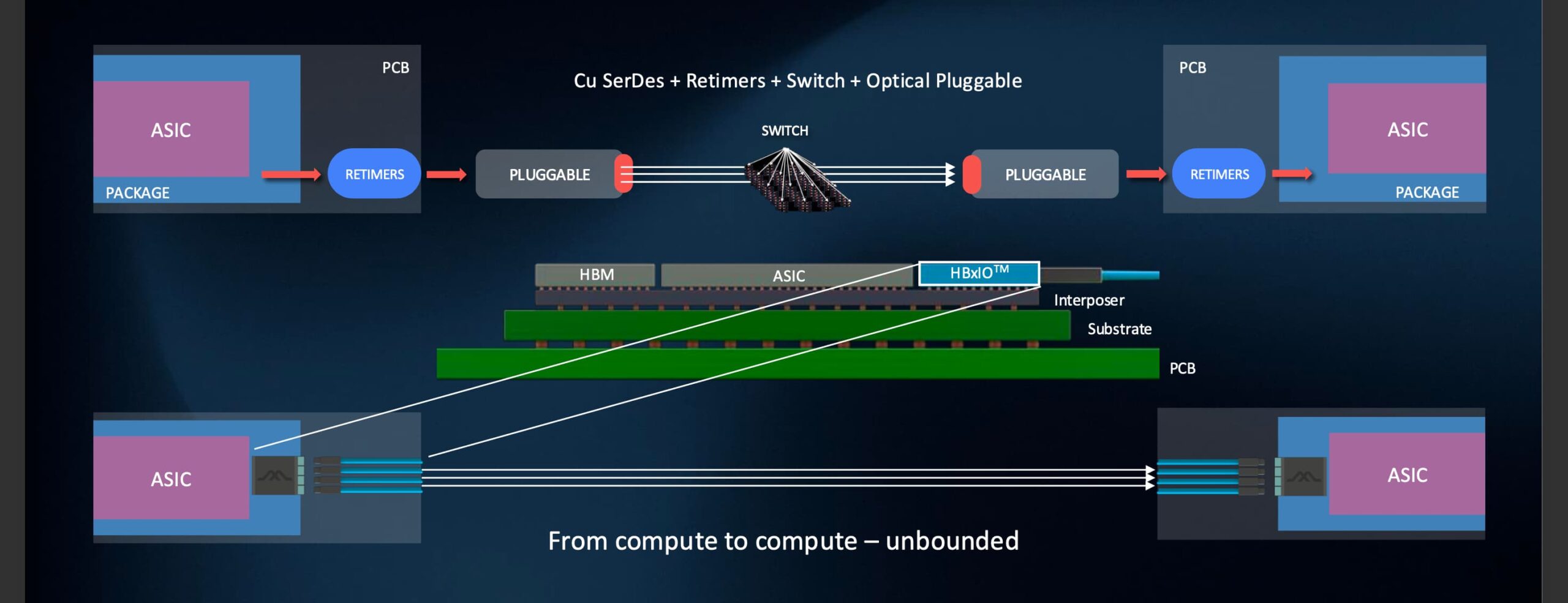
The 500-meter limit stems from pragmatic engineering. “The reach can be provided by high-power lasers, while still being within the spectrum of what is available at the right cost and the right reliability,” says Raghuraman.
Pushing the reach further narrows the choice of viable lasers—a non-starter for hyperscalers prioritising supply-chain robustness.
Modulators and manufacturability
Mixx uses Mach-Zehnder interferometer modulators for its optical engine, rather than the compact ring resonators favoured by firms such as Ayar Labs and Nvidia.
Mach-Zehnder interferometers are bulkier, but Mixx says its design is optimised for high-density silicon photonics. “The Mach-Zehnders fit within that beachfront density,” says Raghuraman. “Bulkiness is all an artefact of how Mach-Zehnder in the past have been used in optical transceivers; we can leverage CMOS-scale technologies to bring effective performance.”
The Mach-Zehnder interferometer modulator also suits thermally sensitive environments such as next to GPUs while meeting interoperability and standards requirements.
The start-up is also claiming a 72 per cent reduction in a typical AI cluster’s power consumption. This stems from multiple factors. By enabling higher compute usage—reducing GPU idle time through faster data delivery—overall system power consumption drops. Eliminating retimers and signal-conditioning circuits also helps, reducing the link to 5 pJ/bit. “We are making it interoperable to standards,” he says.
Link-budget savings of nearly 4dB are achieved through optimised fibre connectivity—a core innovation. “Every dB saves power, whether on the laser or recovery circuits,” says Raghuraman.
This connectivity approach tackles manufacturability at semiconductor volumes. Mixx has developed a bottom-up solution to be compatible with semiconductor flows. The start-up highlights how it has eliminated optical epoxies and UV curing to survive 300°C+ assembly temperatures, while also maintaining optical alignment.
“We had to come up with a technology that works with the true semiconductor manufacturing ecosystem,” says Raghuraman. “We focused on what it takes to develop a solution that is truly manufacturable at scale.”
System-Level Thinking
Beyond hardware, Mixx has developed software, called GuardBand, that handles orchestration between GPUs. “How we enable this orchestration between the GPUs is all done by GuardBand, software that integrates with the network operating system that gives the controllability, observability, and all the telemetrics needed to manage the data movement within the cluster.”
The platform will support standard protocols at the fibre level- Ethernet, Ultra Ethernet, InfiniBand- while die-to-die interfaces can use UCIe or custom protocols. This ensures backwards compatibility and broad integration—whether for scale-up (massive single clusters), scale-out (distributed), scale-in (disaggregated memory/compute), or scale-across (long-reach).
Market dynamics
Mixx is using the funding round to accelerate engineering-sample delivery—primarily of the HBxIO chiplet—for customer integration into custom packages.
Company recruitment is also taking place, covering photonics, electronics, advanced packaging, and opto-mechanics. The company has over 50 staff in the US, Taiwan, and India.
Asked about the recent wave of optical interconnect acquisitions – Ciena acquiring Nubis, and Marvell’s just-completed acquisition of Celestial AI – Mixx’s view is AI interconnect is nascent. “There is no one technology that is going to be the solution,” says Raghuraman.
Tackling the issue from a system perspective rather than at the device level is what differentiates Mixx, says Raghuraman. “We thought about the system level, and then we are targeting building products that satisfy that system.”
AI inference demands underscore the start-up’s focus: low time-to-first-token and inter-token latency. “These two are the fundamentals that are going to be extremely critical for inference,” he says.
Schaevitz also notes that AI model developments, such as the adoption of a mixture-of-experts, mirror the human brain in having localised processing, yet like the brain, there is a need for a central database.
“That’s where connectivity is still going to grow,” says Schaevitz. “The more the ‘experts’ are scattered around, the more that this sloshing of data is important, because otherwise you’re waiting.”
Mixx will give a progress update at the upcoming OFC show in March. The company is working with select partners to build tier-one ecosystems that lower barriers to hyperscaler adoption.
“Most important for hyperscalers is the barrier to entry,” says Raghuraman. “We chose to solve one fundamental problem and leverage qualified technologies, where volume data is available.”
Mixx’s system, manufacturability, and efficiency-driven strategy aims to unlock the next phase of AI intelligence: large clusters with reduced power and latency that keep pace with evolving models.
Teramount Races to Scale Fibre-to-Chip Coupling
The start-up raised $50 million in 2025, funding that will move the company from pilot shipments to high-volume manufacturing of its optical input-output (I/O) interface technology.
Teramount is advancing its fibre-to-chip coupling technology toward volume manufacturing. The start-up is targeting the emerging co-packaged optics (CPO) market, where photonics is integrated directly with a chip to improve speed and energy efficiency.
The company has developed a way to attach fibres to a chip suited to semiconductor manufacturing.
The start-up’s focus is to match its interface to the process steps across the supply chain—at photonic chip foundries and outsourced semiconductor assembly and test (OSAT) houses.
The $50 million funding advances Teramount’s plans, says Hesham Taha, CEO of Teramount, to enable optical connectivity for use in advanced AI computing systems.
Wideband surface coupling
Teramount’s core intellectual property connects fibre to a chip’s surface without the bandwidth penalties associated with conventional surface coupling.
In silicon photonics, “surface coupling” is often shorthand for a grating coupler. Teramount’s approach uses what it calls a photonic bump — a coupling and packaging construct integrated into a semiconductor-style process flow — that delivers a wide optical bandwidth with the advantages of surface-mount packaging.
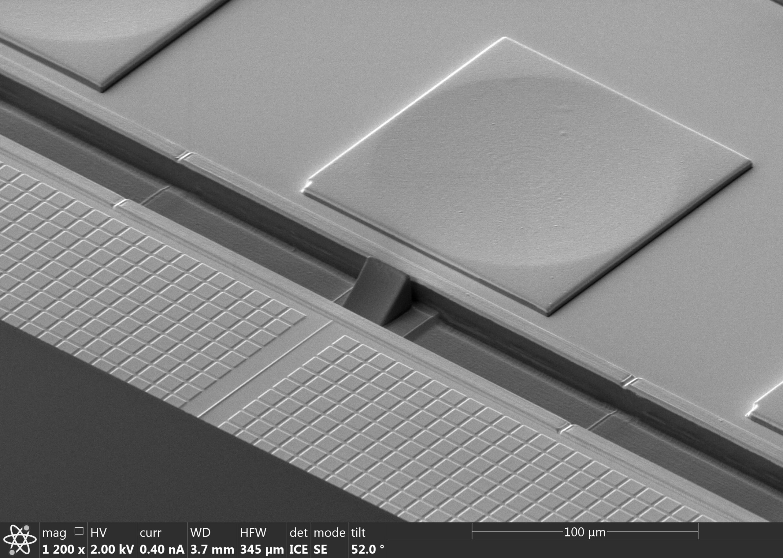
Surface coupling is attractive to photonic chip designers because it eases some of the geometric and packaging constraints of attaching fibres to a chip’s edge. This is becoming more important as systems push toward higher aggregate fibre counts, denser packaging, and tighter link budgets.
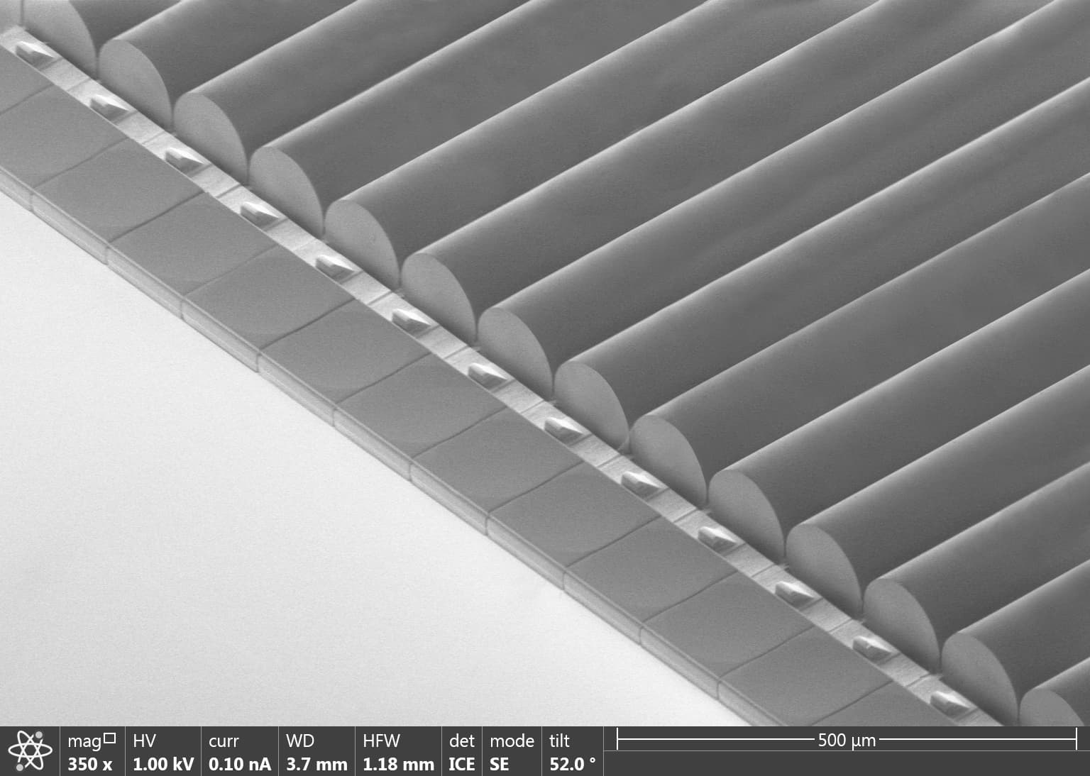
Teramount argues that its bump-based approach can reduce the bandwidth/efficiency trade-offs that start to dominate when designers scale fibre counts and power budgets.
“Our philosophy has been that we needed to bring optics to speak the same language as semiconductor manufacturing,” says Taha. “This is the purpose of our photonic bump.”
Product and positioning
Companies are evaluating Teramount’s TeraVERSE surface-mount fibre-attach product which is now sampling.
Teramount is pursuing more than one on-ramp into silicon photonics packaging and says its approach supports co-packaged optics for scale-out and for scale-up architectures once the industry is ready to replace copper interconnects with optics for short reaches (1-3m).
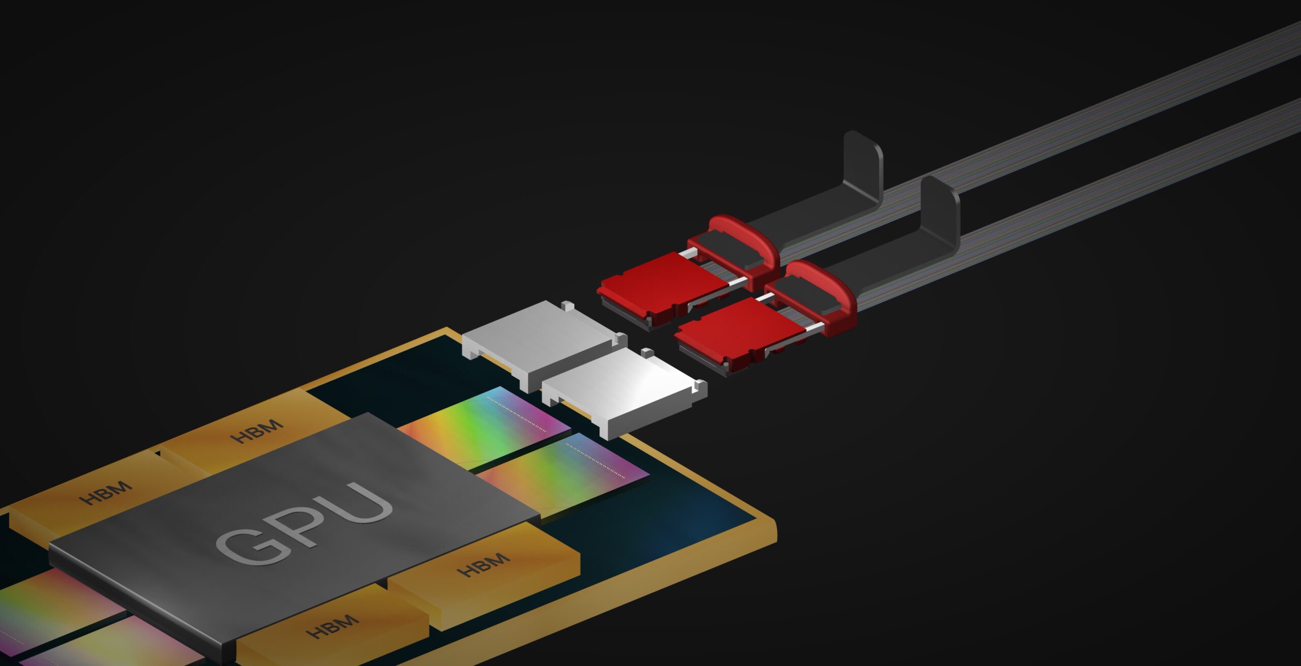
The start-up has a roadmap that enables fibre stacking to increase attach density—an important lever in co-packaged optics-where fibre routing becomes a constraint.
The company says its units are being integrated into silicon photonics wafers at multiple foundries, assembled at major OSATs, and delivered through partner and customer flows aimed at co-packaged optics programmes.
Such integration is challenging. Once optics moves inside advanced packages, alignment tolerances, reflow compatibility, thermal and mechanical stress, and test strategy, all must be addressed in a production setting. Teramount argues the ecosystem is learning these lessons in real time, with system requirements evolving rapidly.
“Customers are asking to increase the number of fibres, increase the optical power, and meet harsh environmental conditions,” says Taha. “Every vendor needs to accommodate these changes on the go.”
Taha also highlights other challenges: fibre management inside the system, accommodating single-mode and polarisation-maintaining fibre where required, and the practical question of “who owns what” when optics meets the chip industry’s established division of responsibilities.
New customers used to volumes
For Teramount, the most consequential change is the nature of the customer. When leading semiconductor companies—AI accelerator and switching players—come to a foundry with a co-packaged optics requirement, it forces engagement at a different level than photonics start-ups can drive.
“The main change is the ownership of the co-packaged optics,” says Taha. “It’s a chip company that is now coming to a foundry for co-packaged optics—and the volumes are going to be high.”
By volume, the expectation is millions of units per year. The company says it is targeting that capability for the middle of 2027.
This shift matters because foundry process tweaks, OSAT line development, supply-chain readiness, and reliability qualification move faster when a high-volume chip programme is the driver.
Manufacturing ramp
Teramount’s Series A funding is aimed at accelerating production plans, expanding suppliers and foundry engagements, and building internal capability to manage a volume transition.
Today, the company operates a pilot-line approach that uses distributed equipment across local and global suppliers, but Teramount is moving toward a consolidated and scalable flow. “We are gathering equipment to have the line in one place,” says Taha.
Teramount says it has grown its staff by half in 2025 to 60, with hiring focussed on operations and manufacturing expertise aligned with high-volume semiconductor making.
There is no one standard for co-packaged optics but eventually the market will settle on a de facto approach, says Taha.
Teramount is effectively betting that manufacturing readiness is a differentiator—and that wideband surface coupling, if it can be packaged and produced like microelectronics – can be part of the co-packaged optics wave that will ship at scale.
Meanwhile, Teramount is aligned with what a key industry transition looks like: a $50 million funding round pointing straight at an important volume manufacturing bottleneck.
Backers of Teramount’s Series A funding round include Koch Disruptive Technologies (KDT), AMD Ventures, Hitachi Ventures, Samsung Catalyst Fund, Wistron, and Grove Ventures.

Ayar Labs prepares to fulfil its optical input-output (I/O) vision

Ayar Labs progresses towards volume manufacturing of its TeraPHY optical input-output (I/O) chiplet.
It is a decade since Vladimir Stojanovic was co-author of a paper published in the science journal, Nature, outlining the first microprocessor to send and receive data optically.
“For the first time, a system – a microprocessor – has been able to communicate with the external world using something other than electronics,” said Stojanovic, then an associate professor of electrical engineering and computer science at the University of California, Berkeley
Ten years on, silicon photonics and optics packaged alongside silicon have come a long way.
Broadcom has added its third-generation co-packaged optics design to its 102.4 Terabit-per-second (Tbps) Tomahawk 6 switch chip. And Nvidia has announced two families of switches, its first, that use the optical technology.
Co-packaged optics has long been promoted as lowering power consumption and aiding processing scalability. But in the last year it has proven to be far more reliable than traditional pluggable optics.
Ayar Labs, too, has come a long way, a start-up Stojanovic co-founded and which, since 2024, has been its chief technology officer (CTO). In 2025, Ayar Labs detailed its third-generation TeraPHY optical I/O chiplet, first in a post-deadline paper at OFC 2025 and then at the Hot Chips 2025 event this summer.
The start-up has also announced partnerships with Taiwanese ASIC design companies, Alchip Technologies and Global Unichip Corp (GUC), both with strong links with leading foundry, TSMC.
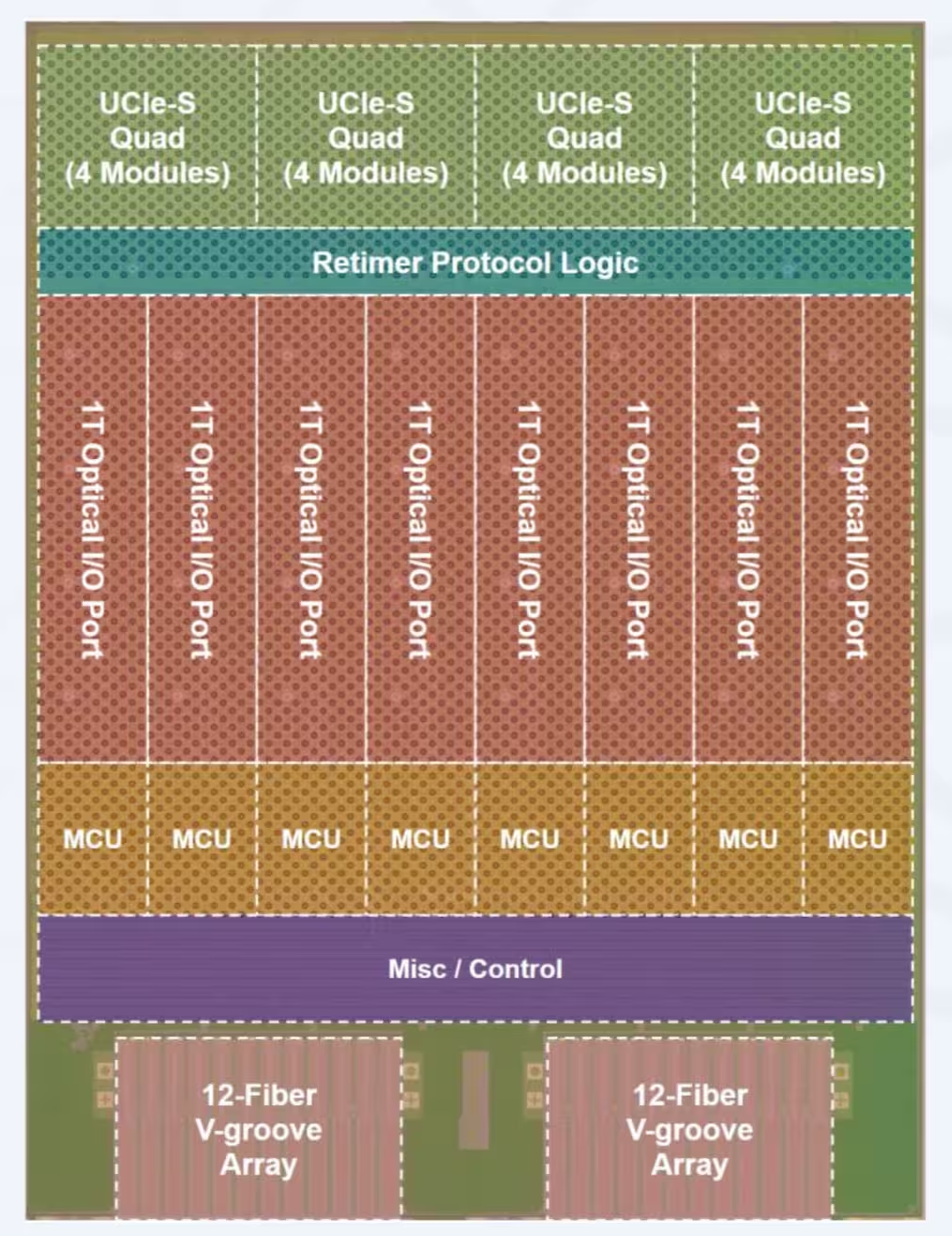
Third-generation TeraPHY optical I/O chiplets
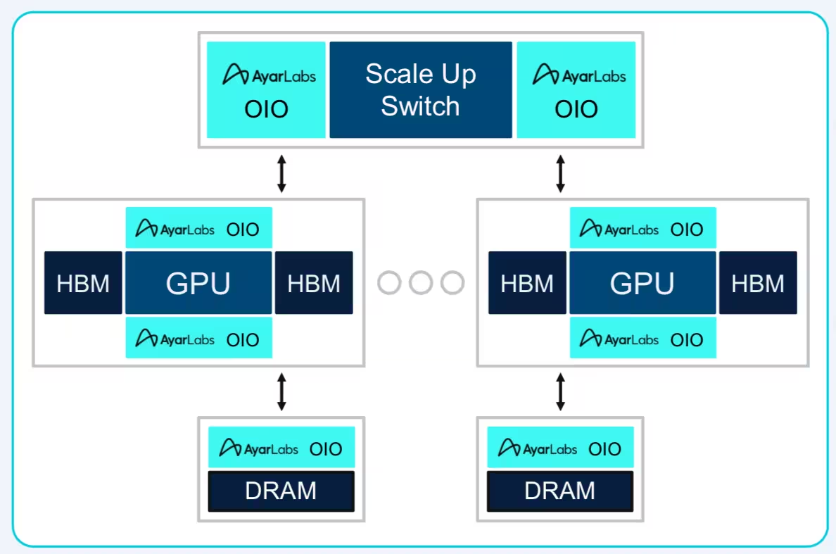
The latest TeraPHY optical I/O chiplet has a bidirectional bandwidth of 8Tbps, or 4Tbps in each direction (see diagram above). It is also the first chiplet design to carry Universal Chiplet Interconnect Express (UCIe) traffic optically. UCIe is a standard die-to-die protocol and Ayar Labs has extended its reach using light. UCIe can carry various protocols and Stojanovic describes the latest device as a ‘universal I/O chiplet’.
The chiplet uses eight 1Tbps optical ports, each supporting 512Gbps channels per direction. Each wavelength carries a 32Gbps signal and using 16 silicon photonics micro-ring resonators, there are 16 wavelengths per fibre.
Ayar Labs also makes a custom-designed laser module – the external light source – that powers the TeraPHY optical I/O chiplets. Dubbed the SuperNova light source, the module uses an array of distributed feedback (DFB) lasers provided by Sivers Photonics.
Ayar Labs uses Sivers’ DFB cell and has adapted it to create a laser array packaged in a module, with the lasers multiplexed and split into wavelengths.
A SuperNova module can have 8 or 16 ports, each with 16 wavelengths, for a total of 128 or 256 wavelengths.
From monolithic optics to modular chiplets
Ayar Labs is a fabless company, meaning it can choose a fab for its design to deliver the best performance and cost. “And in an appropriate ecosystem where our customers want to build their solutions,” adds Stojanovic.
“This [TeraPHY optical I/O chiplet] architecture lets us move seamlessly through different foundry processes,” says Stojanovic. “We can adopt the best CMOS node for logic while keeping the photonic building blocks stable.”
The 8Tbps TeraPHY device is built using GlobalFoundries’ 45SPCLO 45nm silicon-photonics process — a platform that Ayar Labs helped shape. But the design can also be migrated to TSMC’s more advanced CMOS nodes for the electrical IC while benefiting from TSMC’s silicon photonics and packaging flows.
Universal I/O chiplet
Each generation of Ayar Labs’ optical I/O engine follows the same architecture: a modular optical chip with a die-to-die interface, logic in between, and an optical serialiser/deserialiser (serdes) core.
The optical serdes carry the UCIe protocol. What that does, Stojanovic explains, is eliminate the electrical serdes from any connection between two chips — say, GPU-to-GPU or a GPU to a switch. “Each side runs a low-power UCIe interface that connects a few millimetres to our chiplet, and from there it can go anywhere in the system,” says Stojanovic.
The two GPU endpoints operate as if within one package – the definition of a scale-up architecture – creating what he calls the illusion of a single, massive GPU. This makes UCIe a fabric not just for multi-die packages but for multi-module systems, without changing how the GPUs or accelerators see each other.
On the optical side, each of the 16 wavelengths are spaced 200GHz apart, providing terabit aggregate bandwidth, with each port multiplexing and demultiplexing these wavelengths.
Ayar Labs has shown that the high wavelength count works over standard single-mode fibre over tens to hundreds of metres. “You can now run 30, 50 or even 100 metres without polarisation-maintaining fibre,” he says. “That’s essential if you want to scale clusters economically.”
The chip is protocol-agnostic. It can carry CXL, NVLink, UALink, Ethernet or other traffic, encapsulated in the UCIe streaming raw mode.
“Our chiplet never looks at what’s inside,” Stojanovic says. “It just gives the illusion that you’re talking over a wire to the chip next to you.”
This makes the device a universal building block for GPUs, switches, or memory controllers. With per-chiplet bandwidths now reaching multiple terabits per second, Ayar positions its design as a logical successor to high-speed electrical I/O.
“The UCIe scaling roadmap is faster than high-bandwidth memory (HBM),” he notes, “so we can reach or exceed HBM-class bandwidth per chiplet.”
Scale-up first, extended memory next
The first commercial use of the technology will be for GPU scale-up architectures that connect accelerators within and across racks. “That’s the natural order of things,” says Stojanovic. “Optics is clearly becoming valuable for scale-up and multi-rack domains.”
The next step will be to link GPUs to extended memory (see diagram above). Using the same universal I/O chiplet, designers can partition bandwidth between inter-GPU communication and memory traffic depending on workload. “That lets you tailor performance efficiency — teraflops per watt — as well as interactivity [for inference],” he says.
The common element across both applications is flexibility: one optical die serving multiple system roles.
From racks to ‘islands’
Stojanovic expects that optical I/O will help expand the number of AI accelerators in a scale-up domain before scale-out becomes necessary.
“A single switch can’t have a radix much higher than about 512,” he explains. “With multi-die GPU packages, you can reach about 1,000 GPU dies per domain today, and in the next few years, we’ll see clusters of 1,000 to 10,000 GPU dies acting as one.”
He describes these as high-speed optical islands — units that operate as a single accelerator within a data-centre-scale cluster. “If you have 1,000,000 GPUs in a data centre, it’s a hundred islands of 10,000,” he says.
Optical I/O helps solve the key limitation of electrical networks: switch congestion. “In two-stage Clos networks, congestion is the problem. If you have plenty of bandwidth, you can enable path diversity — multiple switch planes — which dramatically reduces latency. An uncongested switch traversal is a few hundred nanoseconds.”
In effect, the bandwidth abundance that optical I/O delivers becomes a new lever for scaling compute clusters without compromising efficiency or latency.
Manufacturing and partnership
To bring the chip into high-volume manufacturing, Ayar has partnered with Alchip Technologies, a leading ASIC design house closely tied to TSMC. Alchip designs advanced ASICs and packages for hyperscalers and will integrate Ayar’s optical engines directly into compute or switch packages.
“When you make an optical engine, you need to put it in an advanced package — an xPU or switch package,” Stojanovic explains. “Alchip has the experience and market access in hyperscale. Together, we can provide a packaged ASIC decorated with optical engines that’s ready to connect at cluster scale.”
This arrangement, he adds, “helps hyperscalers de-risk deployment. The product is manufactured in a high-volume flow certified by TSMC, tested and qualified in that ecosystem.”
Ayar Labs is also partnering with a second leading Taiwanese ASIC player, Global Unichip Corp (GUC), to integrate its TeraPHY optical engine into GUC’s advanced ASIC design services. GUC is an ASIC processing and packaging company, with TSMC as its largest shareholder.
Competing to win
With multiple companies now targeting optical I/O, Stojanovic identifies three factors that will differentiate between the solutions.
“First is being in the right ecosystem — access to the best foundry and packaging partners,” he says. “Second is the form factor. It has to be manufacturable at scale; that’s why we chose chiplets.”
The third is maturity: proven reliability, validated system behaviour, and a roadmap that spans generations. “We’ve qualified our lasers, pushed our previous chips through reliability studies, and done thorough system-level validation. That’s what makes this technology ready for high-volume manufacturing.”
Will AI’s demand for GPUs and interconnect eventually slow? Stojanovic doubts it. “When people talk about slowing down, what that really means is slowing down for the end user,” he says. “Inside, you’re actually speeding up.”
Models may stabilise in size, but inference now chains multiple computations per query. “That means your one computation has to be ten times faster. Interactivity still matters,” he says.
Large clusters will therefore remain essential. “In the next two to five years, you’ll see between one and ten thousand GPU dies working as one in a cluster,” he predicts. “That’s the architecture optical I/O makes possible.”

Interview: Richard Soref, the “founding father” of silicon photonics

Professor Richard Soref, pictured, shares his thoughts on promising areas in photonics.
Richard Soref has been thinking about light in silicon for longer than most photonic engineers have been working in the field.
His wide-ranging interests extend beyond photonics: two decades ago, he published a poetry book titled: “Your Fate.”
Over the course of his career, silicon photonics has moved from a speculative research topic to a foundational technology of modern data centres. Today, however, Soref operates far from the commercial momentum he helped set in motion.
Now approaching his 90th year, Soref no longer manages a research group, nor is his work funded: until recently, he had access to grants. Yet his engagement with photonics, optical computing, and emerging computing paradigms remains active and wide-ranging.
“I don’t rank opportunities,” Soref says. “If something looks interesting, I explore it.”
An eclectic view of photonics
Soref’s broad research interests make for a long list: mid-infrared sensing, optical and optoelectronic computing, artificial intelligence (AI) acceleration, and terahertz systems.
That breadth reflects a career spent moving between materials, wavelength regimes, and applications rather than following a single roadmap.
This is how he came to see silicon as a promising material for light.
In 1985, the only photonic chip that could interface to fibre was the III-V semiconductor chip. Soref wondered if a silicon chip could be used, and whether it might even do a better job.
He had read in a textbook that silicon is relatively transparent at the 1.30- and 1.55-micron wavelengths used for telecom, which inspired him to look at silicon as a material for optical waveguides.
Silicon promised the potential of using the chip industry’s advanced manufacturing infrastructure for electro-optical integration, and aligned with Soref’s interest in materials.
“I’m a science guy, and I have curiosity and fascination with what the world of materials offers,” he told Gazettabyte a decade ago. “If I have an avenue like that, I like to explore where the physics takes us.”
Silicon photonics and AI data centres
One current interest is the intersection of silicon photonics and AI infrastructure. The rapid scaling of AI workloads has placed unprecedented strain on data centres in terms of power consumption and data movement.
For Soref, it is not whether photonics will matter, but how it will be incorporated.
“Photonic analogue neural computing should be deployed alongside electronic GPUs,” he says. “They should share the computing tasks.”
In a recent multi-author paper, Soref and colleagues propose large-scale opto-electronic neurons capable of implementing transformer-based large language models. The approach is not to replace GPUs. Instead, photonic systems would handle specific workloads, offering advantages in processing speed and energy efficiency.
“This combined approach would improve overall processing performance and power efficiency,” says Soref.
The implications are substantial. The paper predicts that such architectures could reduce data-centre power consumption by an order of magnitude. Crucially, the proposed systems rely on optoelectronics manufactured through hybrid bonding to 12-inch (300mm) silicon wafers, aligning with existing semiconductor manufacturing infrastructure rather than requiring exotic processes.
Beyond today’s AI models
Soref is also looking beyond current generative AI systems. He points to emerging ideas such as spatial AI and world models, where machines integrate multiple sensor inputs and interact with physical environments.
“The inputs are not just digital data scraped from the internet,” he says. “They come from sensors—vision and other modalities.”
Such systems, he argues, could place even greater demands on computing efficiency and data handling, making optoelectronic approaches increasingly relevant.
Optical and quantum computing
Quantum computing inevitably enters the discussion. Soref approaches the topic with caution. He does not question its importance, rather he is wary of assuming that quantum systems will dominate future computing.
His exploration is for alternative approaches to quantum, including semiconductor-based single-photon detectors aimed at room-temperature quantum operation.
In a paper published in APL Quantum, Soref and collaborators proposed that by gating computation on nanosecond timescales, the impact of detector dark counts could be mitigated. Dark counts refer to false signals that occur even when no photons are present, a significant source of noise in photonic quantum systems. By using nanosecond timescales, the idea is to “listen” to the photon detectors during tiny windows only when quantum information is expected to arrive.
“It’s a different way of thinking about the problem,” says Soref.
The work has not gained widespread traction, something Soref attributes partly to inertia and to the heavy investment already committed to superconducting approaches. By contrast, he sees optical and optoelectronic computing as closer to engineering reality, even if still technically challenging.
Soref’s work philosophy
A striking aspect of Soref’s work is how he does it. His long history of funding from the U.S. Air Force Office of Scientific Research ended in mid-2025. When the grant expired, he chose not to apply for another. “That was a turning point,” he says.
Today, he works without sponsorship and without institutional affiliation.
He spends his time reading academic papers, scanning arXiv, and following developments across multiple subfields. When something catches his interest, he reaches out directly to researchers.
Some collaborations flourish. Others never begin.
“It’s getting harder,” he admits. “Everyone has their own obligations. I’m not their primary focus.”
Nevertheless, several long-term collaborations continue. In Europe, he has worked for more than a decade with researchers exploring novel photonic structures and materials.
One collaboration with Italian academics focuses on terahertz photonics. Working with colleagues in Italy, Soref has explored topological photonic crystals in silicon designed to guide terahertz waves with low loss and sharp bends.
By integrating phase-change materials and graphene micro-heaters, these structures could act as electro-optical switches at terahertz frequencies. The work is early-stage and largely theoretical, but it exemplifies Soref’s willingness to engage with problems outside mainstream commercial priorities.
Choosing freedom over pressure
Given his long-standing experience, Soref could take on formal advisory roles, industry consulting positions, or editorial leadership posts.
He was recently asked to serve as editor-in-chief of a new journal, but he declined due to the time and responsibilities involved. What he values is flexibility: the freedom to think, explore, and collaborate without managerial or institutional constraints.
But Soref admits he is conflicted. “Part of me wants to keep going with innovation. Part of me wonders whether I should phase out.”
Soref’s other pursuits also take up his time: he likes to travel and is an avid photographer with his work shared online. And it was at the Bread Loaf Writers’ Conference in Ripton, Vermont, where he refined and then published his book of poems.
But for now, he continues—reading, thinking, collaborating, and occasionally publishing—driven not by funding cycles or commercial pressure, but by intellectual curiosity.
“I do this for the intellectual reward,” says Soref.

448G: doing what has been done before may no longer be enough


-
-
-
-
-
PAM-4 may not carry 448G electrical signalling all the way
-
The OIF is leaning toward a reach-dependent roadmap, not one universal solution
-
Optimisation may have to broaden from the SerDes to the rack.
-
-
-
-
The industry keeps progressing in its ability to push more bits down a wire. It has always been challenging to double the transmitted bit rate, but there was headroom to speed up the serialiser/deserialiser (SerDes) circuitry every few years.
But now the OIF, the industry organisation tasked with doubling copper electrical interface speeds to 448 gigabit-per-second (Gbps), must consider more complex techniques and do its work more quickly due to AI’s scaling needs.
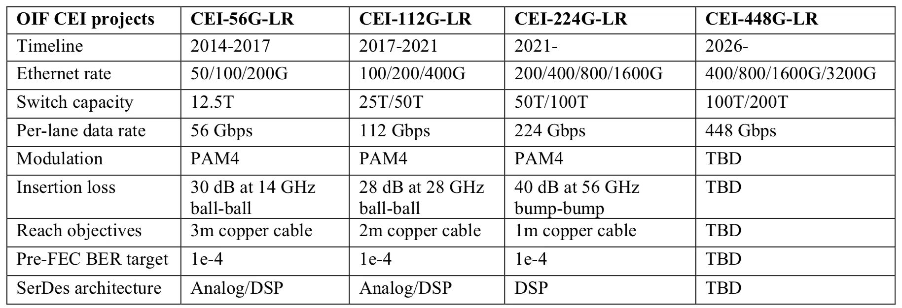
Around a decade ago, the OIF moved from simple non-return-to-zero (NRZ) signalling to 4-level pulse-amplitude-modulation (PAM-4) to double speeds to 56Gbps, known as CEI-56G (Common Electrical I/O). PAM-4 enabled a doubling of the bit rate while using existing 26-28 gigabaud (GBd) components.
PAM-4 was also used for the next two OIF CEI standards, at 112Gbps and 224Gbps. But for the latest 448Gbps standard under development, it is already evident that PAM-4 may not be enough.
When the CEI-448G work began in August 2024, the OIF involved other industry-standard bodies for the first time.
“We collectively understood that 448 gigabit is going to be more challenging for various reasons, including the laws of physics,” says Nathan Tracy, OIF president and technologist, system architecture team at TE Connectivity.
The OIF started pulling together a CEI-448G framework document and circulated it to gain input from various sources. The aim was to galvanise and create a unified position before publishing the document for wider circulation in November.
Delivering reach
The new standard must not only double the data rate from 224Gbps to 448Gbps but also try to retain the reach of previous CEI standards. “That is an exceptional challenge,” says Cathy Liu, the OIF vice president, distinguished engineer and director at Broadcom.
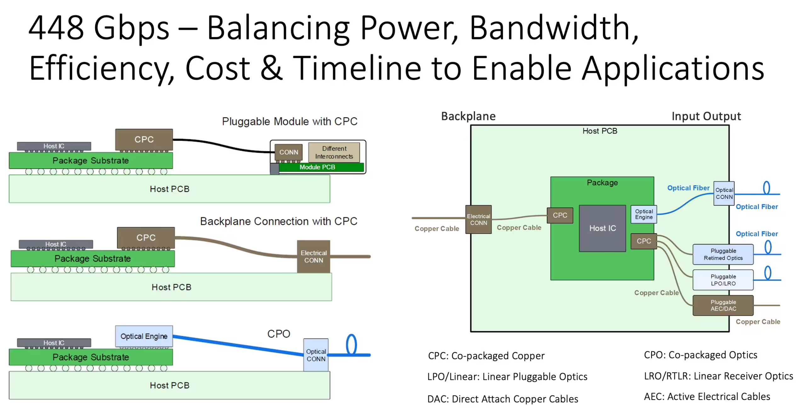
The OIF CEI work involves developing specifications, published as OIF Implementation Agreement documents, for different reaches. The shortest reaches are between dies, between a die and an optical engine within a package, and between separate dies near to each other. These applications fall under CEI-XSR and CEI-XSR+ (extremely short reach interfaces).
Connecting the host chip to a pluggable module requires the OIF’s very short-reach (CEI-VSR) interface. The next reach range is medium reach (MR), typically to connect chips on a printed circuit board.
The most challenging is the Long Reach (LR) spec, which can pass through a backplane to connect chassis in a rack or between adjacent racks. The challenge the OIF faces is that doubling the symbol rate while maintaining the same reach collides head-on with channel bandwidth limits and impairments.
Using PAM-4 at 448Gbps corresponds to a symbol rate of 224GBd, which in Nyquist terms implies a channel bandwidth of 112GHz. The OIF’s work group members have yet to achieve such a bandwidth, but progress is being made.
“Starting in October 2024, we were looking at channels that were rolling off at 75-80GHz; now we’re seeing channels approaching 100GHz,” says Tracy. Still short of 112GHz, but notable progress nonetheless. It also helps clarify the equalisation schemes that will be needed.
One solution is to adopt higher PAM schemes such as PAM-6 or PAM-8 to relax the analogue bandwidth. PAM-6 reduces the baud rate to around 174GBd and the analogue bandwidth from 112GHz to 90GHz, while PAM-8 reduces the baud rate further to 150GBd and a 75GHz bandwidth.
The higher-order PAMs may relax the analogue bandwidth targets but place greater demand on the receiver’s digital signal processor (DSP) tasked with recovering the greater number of bits per symbol.
OIF’s reasoning
The likelihood is that the work will start with the most challenging LR specification. “If we can do the long reach, then we can also support the chip-to-module, the VSR application and XSR, which is more targeted at the co-packaged optics application,” says Liu.
For LR, the aim is to span backplanes and chassis interconnect using copper cables. There will also be work on linear-drive and half-retimed designs, as these promise lower power consumption.
The OIF is cautiously optimistic about reach. “We’ve looked at channels at 400 gigabit that suggest that at least a meter of reach may be possible,” says Tracy. “It’s not a slam dunk; everything that we get will be hard fought for.”
Liu says that reach and low power are almost orthogonal requirements. The OIF challenge, she says, is to come up with solutions that meet these ‘orthogonal’ requirements.
For LR, it requires advances in connectors, equalisation schemes, and forward error correction (FEC) to counter channel impairments.
“Even with the improvement we have seen, there’s still a challenge existing in the channel loss and the crosstalk reflections, which is limited to a bandwidth of 90GHz,” says Liu.
That makes using 448G PAM-4 extremely challenging.
Connecting the host chip to the pluggable module, the OIF is optimistic that over time 120GHz will be possible, but the issue is that solutions are needed sooner. “It’s a very dynamic world we are in,” says Tracy.
Liu outlines that the OIF’s thinking is a staged, reach-dependent strategy that allows the industry to ship something soon to meet AI’s demanding networking needs even as channel limitations persist.
Liu outlines a world where different reaches adopt different solutions: PAM-4 may be possible for shorter reaches, while higher modulation schemes – PAM-6 or PAM-8 – may be required for longer reaches, considering the 90GHz channel reality.
The OIF stresses this is not yet policy. “We maybe diverge based on the different application spaces, the debating is still happening,” says Liu. But hard calls are approaching.
Crucially, Liu points out that the issue of backward compatibility will change if the industry adopts higher-order PAM schemes soon. Indeed, she argues it is an advantage if the OIF starts with higher-order PAM now because if channels improve later, the transition to future speeds (CEI-896G?) will be smoother.
“Don’t assume the ‘lowest PAM wins’ permanently—sometimes the industry keeps a higher-order scheme because it becomes a stepping-stone to the next throughput jump,” says Liu.
If a higher-order PAM is adopted, the need for more DSP assistance will be helped by continual advances in CMOS process nodes.
“When you’re using the higher modulation schemes, you can reduce the baud rate, so the analogue is easier, but then more complicated detection is needed,” says Liu. Yet more gates are a byproduct of more advanced CMOS nodes. So, putting the burden on the DSP rather than the analogue bandwidth may be the better approach.
About FEC schemes, Liu acknowledges the classic trade-off: higher modulation schemes require more advanced FEC, but the key is not to overdo it, as the price is greater power consumption.
The rack as a unit of optimisation
Tracy notes that the decisions regarding 448G can’t be evaluated just from a SerDes perspective since the optimisation target is shifting upwards.
“We need to think about the rack as the smallest building block that matters instead of thinking about host silicon,” says Tracy.
At this higher system scale, trade-offs may invert: “If we increase power dissipation a little bit at the silicon level, but at the rack level, it gives us a lower aggregate power, then that’s an important consideration,” he says.
That’s the subtext behind the entire 448G framework: the industry is choosing not just an electrical interface, but an evolution path for in-rack architecture under three key constraints, says Tracy. The first is a physical one – the bandwidth, reach, and noise, the second is economic: cost and power consumed, and the third is operational: deploying not just at scale but hyperscaler scale.
The pressure to move fast is already here: “Truly, the time is upon us,” says Tracy.

Books of 2025: Part 3
Gazettabyte is asking industry figures to pick their reads of 2025. In Part 3, Professor Martijn Heck, Brad Booth, Matthew Crowley, and Neil McRae share their choices.
Professor Martijn Heck, Photonic Integration, Eindhoven University of Technology
Why do I read? When I was a kid, I loved history and read a lot of history books and biographies. Napoleon and William of Orange were my favourites. At the age of 11, I fell in love with fantasy after my father introduced me to The Lord of the Rings. Later, my interest expanded to literary historical mysteries, such as the works of Monaldi & Sorti, Charles Palliser, and Matthew Pearl. But at the same time, one of my greatest joys of returning to Eindhoven after working 11 years abroad was that I could visit Eppo Strips again, our excellent local comic book store, to enjoy the art of a comic book.
So, what did I read last year that I would recommend? Elon Musk mentioned that Foundation by Isaac Asimov was one of his primary inspirations. It’s a classic that I never read, but my fascination (not adoration) with Musk pulled the trigger. It’s about the decline of the Galactic Empire and how an outcast group preserves knowledge and technology, using them to build a power base. Quite a lot of parallels with the current state of our world, and the fact that this is one of Musk’s favourites, should, maybe, ring alarm bells.
This year, Jan Terlouw died, one of the Netherlands’ most erudite and well-loved former politicians. He also wrote children’s books.
Well, young adult fiction, as we call it nowadays. After reading too many literary, complex-character, development novels, I started missing a simple element: a story. How to Become a King (Koning van Katoren in Dutch) offers precisely that. A boy needs to solve seven impossible tasks to become king. Sounds like a Grimm fairy tale, but has a contemporary message, covering issues from religious conflicts to environmental pollution. I think the world needs to read more children’s books to make big problems unequivocally clear and solve them.
Talking of religions, Small Gods: A Discworld model by Terry Pratchett should also be mentioned. It is a satire on religion and philosophy, which offers a much-needed lightness in a world where people sometimes take themselves far too seriously. Like in academia. And, of course, the author who imagined a disk-shaped world, carried by four elephants who stand on a giant turtle swimming through space, is a welcome source of inspiration for creativity, which is also needed in my profession. I did not see octarine in my optical spectrum analyser yet, though.
Lastly, back to comic books, let me throw you an extra free recommendation: check out Suske en Wiske (I refuse to translate this, for nostalgia reasons), the Blue Series. Great for you and your children.
Brad Booth, CEO of NLM Photonics
It can be challenging when you’re in a start-up to find time to read a book, but I have been working to allocate more time to reading. Previously, many of my reads were in the science fiction genre, such as the Dune series, for entertainment. Lately, though, I’ve been reading a broader range of books to gain different insights and perspectives.
One is Jonathan Haidt’s The Anxious Generation: How the Great Rewiring of Childhood Is Causing an Epidemic of Mental Illness. As someone who grew up before the Internet and smartphones, and then worked in the industry during their development, it was an enlightening read. As a father of two boys who fit within the profile of Haidt’s analysis, it was interesting to see how some of my decisions about access to electronics impacted their lives. My wife worked in the gaming community, where gaming and social media companies discussed player retention and engagement. While that may seem harmless, the impact on the younger generation is obvious today.
As a father and a CEO, I can see how media, social media, the internet, electronic devices, etc., have had a profound impact on our society and, more importantly, on our youth.
As we head into the AI age, I highly recommend this book to any parent or technologist seeking insight.
Another book that I’ve almost finished reading is Elmer Kelton’s “The Time It Never Rained.” It is a fictional account based on a long Texas drought that occurred in the 1950s. The story focuses on a rancher in West Texas and covers topics such as government subsidies, government intervention, prejudice, illegal immigration, and weather impacts on farmers and ranchers. While the story is set in the 1950s, it is interesting how much of it remains relevant today. It also provides excellent insight into the challenges that face independent farmers and ranchers, sort of like being in a start-up and living from one round of financing to another.
Matt Crowley, CEO of Scintil Photonics
One author I read was Peter Zeihan a geopolitical strategist who has written a series of books starting with the Accidental Superpower: Ten Years On that focusses on how geopolitics has evolved in the post-cold war era and where it is likely to go next.
Focussing on demographic, geographic, and historical trends, his take is worth reading for executives in the semiconductor and AI industries with globe-spanning supply chains and markets.
The modern era requires that executives, investors and analysts to consider geopolitical impacts on their business much more than in the past.
The second book that I enjoyed was BlindSight, by Peter Watts which in a philosophical sci-fi space adventure that explores our ideas of consciousness and intelligence through the lens of a group of humans with augmented intelligence encountering a truly alien intelligence that challenges ideas about intelligence, cognition and consciousness that are highly relevant to today’s debates about LLMs, AGI and how LLM augmented human cognition will evolve in the coming years.
Neil McRae, Chief Network Strategist at Juniper Networks.
There’s Got to Be a Better Way: How to Deliver Results and Get Rid of the Stuff That Gets in the Way of Real Work, by Donald C. Kieffer & Nelson P. Repenning is one of those rare leadership books that made me think, “Of course!”
It’s practical and insightful. We’ve all been in organisations that work harder but not smarter, usually because we’re busy treating the side effects rather than addressing the underlying problems. We also tend to assume work is static, when in reality it’s massively dynamic. And who hasn’t sat through the meeting where all the metrics are green, yet the project is months behind?
The authors introduce Dynamic Work Design, anchored in five principles: Solve the right problem – Structure for discovery – Connect the human chain – Regulate for flow – Visualise the work.
They expand on this through ideas such as using effective problem-solving tools (like System Dynamics), ensuring day-to-day work reveals where the next issue will come from, connecting the people who are best positioned to solve those problems, avoiding system overload, and making sure work is visible as it moves. It sounds simple, but it’s remarkable how few organisations operate this way. Too many try to push more through the system than it can handle, and far too many rely on metrics that hide opportunities for improvement rather than reveal them.
Crucially, the authors argue—and I fully agree—that it starts with leaders getting out of their offices. Leaders need to get onto the shop floor, understand the real work, strip away the noise, and get close to the actual metrics. By rolling up their sleeves, they build trust, create alignment, and foster a culture where people talk openly and in real time about problems and how to solve them. When progress is made visible, people can feel that things are getting better.
I can’t help but feel the telco industry, in particular, could benefit enormously from this kind of approach.
Overall, *There’s Got to Be a Better Way* is an outstanding read for anyone trying to build healthier, more effective organisations. It’s thoughtful, grounded, and refreshingly honest. I’d recommend it to leaders, managers, and anyone who’s ever wondered why good intentions so often collide with organisational reality, and how to close the gap between leaders, employees, and the work itself.