
PCI Express back on track with latest specifications
Richard Solomon and Scott Knowlton are waiting for me in the lobby of a well-known Tel-Aviv hotel overseeing the sunlit Mediterranean Sea.
 Richard SolomonSolomon, vice chair of the PCI Special Interest Group (PCI-SIG), and Knowlton, its marketing working group co-chair, are visiting Israel to deliver a training event addressing the PCI Express (PCIe) high-speed serial bus standard.
With over 750 member companies, PCI-SIG conducts several training events around the world each year. The locations are chosen where there is a concentration of companies and engineers undertaking PCIe designs. “These are chip, board and systems architects,” says Solomon.
PCI-SIG has hit its stride after a prolonged quiet period. The group completed the PCIe 4.0 standard in 2017, seven years after it launched PCIe 3.0. The PCIe 4.0 doubles the serial bus speed and with the advent of PCIe 5.0, it will double again.
“We were late with PCIe 4.0,” admits Solomon. But with the introduction of the PCIe 5.0 standard in the first quarter of 2019, the serial bus’ speed progression will be back on track. “PCIe 5.0 is where the industry needs it to be.”
The latest training event is addressing the transition to PCIe 5.0. “User implementation stuff; the PHY, controller and verification IP,” says Knowlton. Verification IP refers to the protocols and interfaces needed to verify a PCIe 5.0-enabled chip design.
Markets
PCIe is used in a range of industries. In the cloud, the serial bus is used for servers and storage.
For servers, PCIe has been adopted by general-purpose microprocessors and more specialist devices such as FPGAs, graphics processing units and AI hardware.
The technology is also being used by enterprises, with PCIe switch silicon adopted in data centres to enable server redundancy and failover.
PCIe 5.0 is where the industry needs it to be
PCIe is also being used for storage and in particular solid-state drives (SSDs). That is because PCIe 4.0 transfers data at 16 gigabit-per-second (Gbps) per lane and can be scaled in parallel, typically in a by-four (x4) or a by-16 (x16) lane configuration.
The proportion of the SSDs that use PCIe is expected to grow from a quarter in 2018 to over three quarters in 2022, according to Forward Insights. Meanwhile, IDC forecasts that the SSD market will grow at a compound annual growth rate of 15 percent from 2016 to 2021.
PCIe is also employed within mobile handsets and for the Internet of Things designs. PCI-SIG attributes its adoption for these applications due to its speed and lane-width flexibility as well as its power efficiency.
 Source: PCI-SIG
Bus specifications
The PCIe bus uses point-to-point communications. The standard uses a simple duplex scheme - serial transmissions in both directions that is referred to as a lane. The bus can be bundled in a variety of lane configurations - x1, x2, x4, x8, x12, x16 and x32 - although x2, x12 and x32 are rarely, if ever, used in practice.
 Scott KnowltonThe first two iterations of PCIe, versions 1.0 and 2.0, delivered 2.5 and 5 gigatransfers-per-second (GT/s) per lane per direction, respectively.
A transfer refers to an encoded bit. The first two PCIe versions use an 8b/10b encoding scheme such that for every ten-bit payload sent, only 8 bits are data. This is why the data transfer rates per lane per direction are 2Gbps and 4Gbps (250 and 500 gigabytes-per-second), respectively (see table).
With PCIe 3.0, the decision was made to increase the transfer rate to 8GT/s per lane based on the assumption that no equalisation would be needed to counter inter-symbol interference at that speed, says Solomon. However, equalisation was needed in the end but that explains why PCIe 3.0 adopted 8GT/s and not 10GT/s.
Another PCIe 3.0 decision was to move to a 128b/130b scheme to reduce the encoding overhead from 20 percent to just over 1 percent. This is why the transfer rate and bit rate are almost equal from the PCIe 3.0 standard onwards (see table).
The recent PCIe 4.0 specification doubles the transfer rate from 8GT/s to 16GT/s while PCIe 5.0 will achieve 32GT/s per lane per direction.
When more than one lane is used, the encoded data is distributed across the lanes. A PCIe controller is used at each end of a lane to make sense of the bits. Meanwhile, a PCIe switch, a separate chip, can be used when fan out is needed to distribute the point-to-point links.
Compliance testing and design issues
Compliance testing of PCIe 4.0 will only occur in the beginning of 2019 even though it was standardised in 2017. Solomon says that this length of time is actually one of PCI-SIG's shorter periods. It takes time to refine the exact electrical testing to be used, he sys, and there is only so much that can be done until the silicon arrives.
Given that there are now 28Gbps and 56Gbps serialiser-deserialiser (serdes) technologies available, why were the PCIe 4.0 and PCIe 5.0 lane speeds not faster? Solomon says the latest PCIe standards were chosen to be multiples of the PCIe 3.0’s 8GT/s lane speed to ensure backward compatibility.
That said, designing systems using PCIe 4.0 and PCIe 5.0 signalling speeds is a challenge. Printed circuit boards need to be multi-layer and used higher-quality materials while retimer ICs are needed to achieve signal distances of 20 inches.
Solomon stresses that not all systems required such signal reaches; the dense electronics being developed for automotives that use AI techniques to make sense of their environment being one such example.
And with that, Solomon apologises and gets up: “I have a session to present”.
Stitching together disaggregated chips
The Optical Internetworking Forum (OIF) has begun work on a 112-gigabit electrical interface to connect chips in a multi-chip module.
The ultra-short-reach electrical interface for multi-chip modules adds to the OIF's ongoing CEI-112G project, started in August 2016, to develop a 112 gigabit-per-second (Gbps) serial electrical interface for next-generation optical modules.
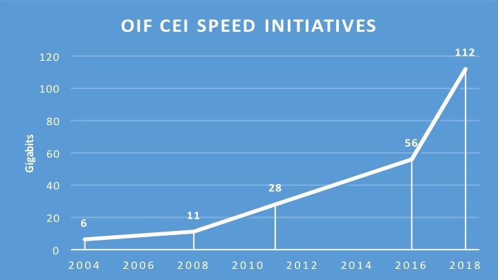 Source: Gazettabyte, OIF data. The year 2018 is an estimate.
The OIF is an industry organisation whose members include telcos, data centre operators, equipment makers and component companies. The OIF undertakes projects that range from high-speed interfaces, optical modules and flexible Ethernet through to programmable interfaces for Transport SDN. Each OIF project culminates in a published Implementation Agreement.
According to David Stauffer, of Kandou Bus and the OIF’s Physical and Link Layer Working Group Chair, the 112G multi-chip module initiative builds on earlier OIF work on a 56-gigabit ultra-short-reach (USR) interface that first addressed die-to-die communication. "We realised that there seems to be more than one application," says Stauffer. "The 112G project is expanded for these applications such that we will possibly end up with different solutions rather than just one."
Multi-chip modules
It was during the 56G USR work that the OIF first heard from members about the challenges of designing a system-on-chip and the idea of taking functions off-chip. High-capacity Ethernet switch chips, for example, are becoming so complex that future designs will not be able to support the long-reach serialisers-deserialisers (SerDes) circuits used for input-output due to the resulting design exceeding the chip's power constraints. “They [chip makers] were starting to think about offloading functions such as SerDes from the system-on-chip,” says Stauffer.
State-of-the-art chip designs can also include functions that occupying significant die area. “To better optimise chip and system costs, people are starting to think about the concept of breaking up the system-on-chip into multiple chips that are better optimised for cost and yield,” says Stauffer. He cites as an example a next-generation system-on-chip that interfaces to long-reach SerDes or optics, performs sensor processing and has significant on-board logic.
 David StaufferThe logic functions of such a chip are best implemented using an advanced 7nm CMOS process, yet SerDes design are not implemented in 7nm and won't be for some time yet. In turn, the sensor array may not even be implemented using a logic process. And if the logic circuitry occupies a significant die area, it may be more economical to split the logic into two chips, each of which will yield better. “Then I have a need for all these interfaces between these chips,” says Stauffer,
He stresses that the interfaces are split based on the the type of technology and on the size of the individual dies; the dies are not partitioned to minimise the bandwidth between them. This can result in significant bandwidth - terabits of capacity - between chips in the module. And to be cost-effective, the interfaces must be very low power.
Accordingly, interfaces between two logic chips or the logic function and the sensor array can require high bandwidth whereas interfaces to the SerDes may be a single lane and have different requirements in how it is clocked. “So there is some divergence in what may be the requirements,” says Stauffer. “The multi-chip module project allows for the fact that we may end up with two solutions.”
The OIF does not list companies involved in its projects. Kandou Bus is clearly one involved in the multi-chip module work, says Stauffer, and he points to similar work his company has done with Marvell but at lower rates. But a recent story in EETimes lists several companies.
Applications
Stauffer says there are several high-performance computing companies that are designing very high-end processing systems using new architectures. “They are going to use this stuff [multi-chip modules and 100G-plus interfaces] before it trickles down to the data centre,” he says.
For applications requiring sensor arrays, the sampling and control loops needed mean that in some cases the interface will need to support terabits-per-second of capacity, says Stauffer; the overall interface speed depending on the number of sensors in the array and the rate at which they sample.
The OIF ultra-short-reach interface is expected to work up to 116Gbps. Some members also want the interface to drive optical devices. “There is going to be a single lane interface at 100G-plus and others that consist of many parallel lanes,” says Stauffer.
The interface will operate over distances of 1cm to 2cm depending on the interposer technology used in the multi-chip module. Using an organic interposer will enable a reach of up to 2cm whereas a silicon interposer the distances will be 1cm or less.
A silicon interposer can be seen as a chip designed solely to interconnect the chips that sit on top, says Stauffer. The advantage of a silicon interposer is that it can supports thousands of input-outputs. But depending on its size and yield, the silicon interposer can be expensive. It also has higher-loss channels, explaining its shorter 1cm reach.
In contrast, an organic interposer is more in line with traditional multi-chip modules, says Stauffer. The interconnect density of an organic interposer is less than a silicon one due to the relatively large pad pitches it uses but the organic interposer is cheaper and has a lower insertion loss. “The OIF is designing something that is suitable for both,” says Stauffer.
No timetable has been given as to the duration of the multi-chip module interface work. But Stauffer says there are companies that would use the electrical interface now if it were available.
FSAN unveils roadmap plans
Part 2: Next-generation passive optical networks
The Full Service Access Network (FSAN) has outlined its vision for fibre access networks for the coming decade.
FSAN is an industry forum that includes over 20 operators and 70 members overall. The group identifies service requirements and develops optical access technologies that are passed to the International Telecommunication Union (ITU) for standardisation.
 Source: FSAN
“One of the messages of the roadmap is that, in the immediate future, what FSAN wants to do is evolve the existing standards,” says Peter Dawes, FSAN NGPON co-chair.
The latest FSAN technologies to become standards are XGS-PON (10 gigabits symmetrical passive optical network) and the multiple wavelength TWDM-PON (time wavelength-division multiplexing passive optical network), also known as NG-PON2 (see chart).
PON status
XGS-PON is a single-wavelength PON standard that supports two rates: a 10-gigabit symmetrical rate and the asymmetrical 10 gigabits downstream (to the user) and 2.5 gigabits upstream originally introduced by XG-PON.
 Peter Dawes
TWDM-PON uses four wavelengths to deliver up to 40 gigabits of symmetrical bandwidth and has an option for eight wavelengths overall. TWDM-PON also uses tuneable lasers enabling operators to move subscribers between wavelengths.
“FSAN operators see continued growth in PON deployment,” says Dawes. “There is still strong deployment of GPON and we are on the verge of needing 10-gigabit symmetrical services.” Other operators may delay and go straight to TWDM-PON, he says.
According to Dawes, operators are seeing a variety of applications that are driving the need for 10-gigabit access rates. One is the growing use of video and video conferencing. Another bandwidth driver for access networks is mobile applications such as connecting mobile antennas and mobile backhaul. In addition, there are digital home trends such as social networking and the moving of content to the cloud.
Mobile fronthaul can eat as much bandwidth as you can supply once you start to aggregate [radio] antennas
Operators are also keen to attach the labels ‘gigabit’ and ‘gigabit services’ to their broadband offerings as a marketing differentiator.
Other drivers for the move to the newer PON technologies include peer-to-peer services and business IP services, says Dawes.
Roadmap
FSAN’s plan to evolve the existing standards in the near term will take the group to 2021.
One obvious way the existing PONs can be evolved is to adopt 25-gigabit wavelengths. This would enable a 25-gigabit symmetrical extension to XGS-PON and a future TWDM-PON variant with up to 200 gigabits of capacity if the full eight wavelengths are used. “It is a case of looking for logical evolutions of these technologies,” says Dawes.
One application that could use such high capacities is mobile fronthaul, says Dawes: “It can eat as much bandwidth as you can supply once you start to aggregate [radio] antennas.”
After 2020, FSAN will investigate disruptive technologies as it defines future optical access schemes. R&D work, new modulation schemes and component developments including silicon photonics will all be assessed as to their suitability for future optical access schemes.
Meanwhile, FSAN says it will review its roadmap on a yearly basis and amend it as required.
See Part 1: XGS and TWDM passive optical networks, click here
Choosing paths to future Gigabit Ethernet speeds
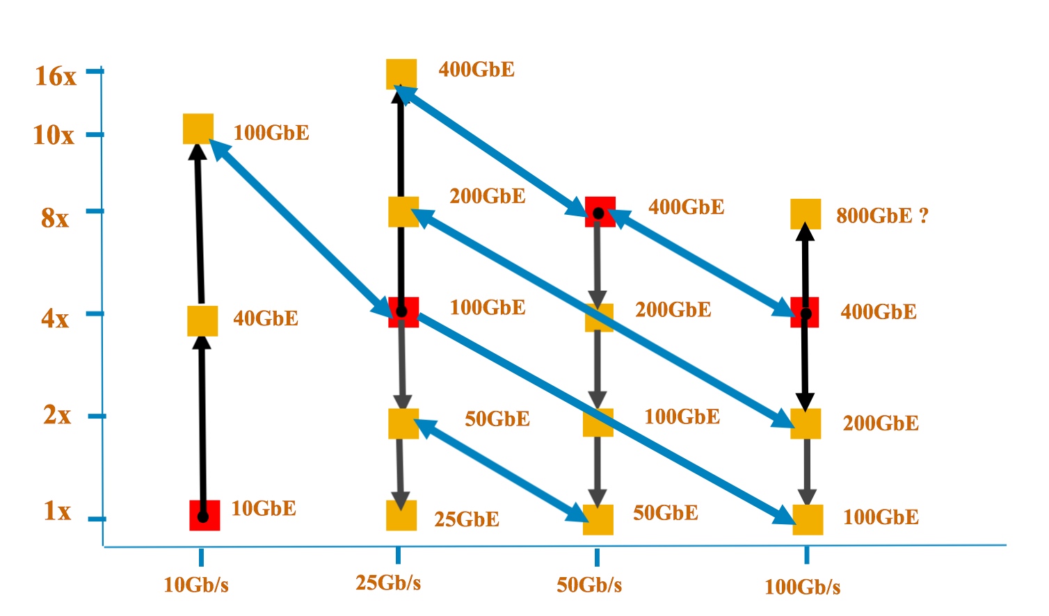 The y-axis shows the number of lanes while the x-axis is the speed per lane. Each red dot shows the Ethernet rate at which the signalling (optical or electrical) was introduced. One challenge that John D'Ambrosia highlights is handling overlapping speeds. "What do we do about 100 Gig based on 4x25, 2x50 and 1x100 and ensure interoperability, and do that for every multiple where you have a crossover?" Source: Dell
One catalyst for these discussions has been the progress made in the emerging 400 Gigabit Ethernet (GbE) standard which is now at the first specification draft stage.
“If you look at what is happening at 400 Gig, the decisions that were made there do have potential repercussions for new speeds as well as new signalling rates and technologies,” says John D’Ambrosia, chairman of the Ethernet Alliance.
Before the IEEE P802.3bs 400 Gigabit Ethernet Task Force met in July, two electrical signalling schemes had already been chosen for the emerging standard: 16 channels of 25 gigabit non-return-to-zero (NRZ) and eight lanes of 50 gigabit using PAM-4 signalling.
For the different reaches, three of the four optical interfaces had also been chosen, with the July meeting resolving the fourth - 2km - interface. The final optical interfaces for the four different reaches are shown in the Table.

The adoption of 50 gigabit electrical and optical interfaces at the July meeting has led some industry players to call for a new 50 gigabit Ethernet family to be created, says D’Ambrosia.
Certain players favour the 50 GbE standard to include a four-lane 200 GbE version, just as 100 GbE uses 4 x 25 Gig channels, while others want 50 GbE to be broader, with one, two, four and eight lane variants to deliver 50, 100, 200 and 400 GbE rates.
If you look at what is happening at 400 Gig, the decisions that were made there do have potential repercussions for new speeds as well as new signalling rates and technologies
The 400 GbE standard’s adoption of 100 GbE channels that use PAM-4 signalling has also raised questions as to whether 100 GbE PAM-4 should be added to the existing 100 GbE standard or a new 100 GbE activity be initiated.
“Those decisions have snowballed into a lot of activity and a lot of discussion,” says D’Ambrosia, who is organising an activity to address these issues and to determine where the industry consensus is as to how to proceed.
“These are all industry debates that are going to happen over the next few months,” he says, with the goal being to better meet industry needs by evolving Ethernet more quickly.
Ethernet continues to change, notes D’Ambrosia. The 40 GbE standard exploited the investment made in 10 gigabit signalling, and the same is happening with 25 gigabit signalling and 100 gigabit.
If you buy into the idea of more lanes based around a single signalling speed, then applying that to the next signalling speed at 100 Gigabit Ethernet, does that mean the next speed with be 800 Gigabit Ethernet?
With 50 Gig electrical signalling now starting as part of the 400 GbE work, some industry voices wonder whether, instead of developing one Ethernet family around a rate, it is not better to develop a family of rates around the signalling speed, such as is being proposed with 50 Gig and the use of 1, 2, 4 and 8 lane configurations.
“If you buy into the idea of more lanes based around a single signalling speed, then applying that to the next signalling speed at 100 Gigabit Ethernet, does that mean the next speed with be 800 Gigabit Ethernet?” says D’Ambrosia.
The 400 GbE Task Force is having its latest meeting this week. A key goal is to get the first draft of the standard - Version 1.0 - approved. “To make sure all the baselines have been interpreted correctly,” says D’Ambrosia. What then follows is filling in the detail, turning the draft into a technically-complete document.
Further reading:
LightCounting: 25GbE almost done but more new Ethernet options are coming, click here