
MACOM acquires Mindspeed to boost 100 Gig offerings
 Ray MoroneyThe Mindspeed acquisition increases the serviceable addressible market for MACOM, both geographical - the company will strengthen its presence in Asia Pacific - and by gaining new equipment vendor accounts. It also broadens MACOM's 100 Gigabit physical device portfolio.
"We are targeting the 100 Gig buildout and the growth coming from that," says Ray Moroney, product line manager, opto-device business unit at MACOM.
Mindpeed also makes a broad portfolio of crosspoint switches used in datacom equipment, and several families of communications processors.
With the acquisition of Mindspeed we have the full electronics bill-of-materials for CFP2 and CFP4 [module] client-side applications
MACOM entered opto-electronics with the acquisition of Optimai in 2011 that had long-haul and client-side modulator drivers and trans-impedance amplifiers (TIAs). Now with Mindspeed's products, MACOM can capture client-side designs with clock data recovery chips and quad-channel TIAs for 100 Gig modules. "With the acquisition of Mindspeed we have the full electronics bill-of-materials for CFP2 and CFP4 [module] client-side applications," says Moroney.
MACOM also gains silicon germanium technology alongside its indium phosphide and gallium arsenide technologies. Silicon germanium has a lower cost structure once a design is being made in volume production, says Moroney, but the R&D and mask costs are generally higher. Silicon germanium also allows significant integration. "It is BiCMOS in nature," says Moroney. "You can integrate full CMOS functionality into a design too." For example digital control can be added alongside analogue functions. Moroney says the company will use silicon germanium for high-performance analogue designs like TIAs as well as high-frequency millimeter wave and microwave applications.
The company is considering its options regarding the future of the communications processors arm of Mindspeed's business. "MACOM is very much an analogue/ RF company," says Moroney. "It [communications processors] is certainly not seen as a core area of investment for MACOM."
Ethernet access switch chip boosts service support
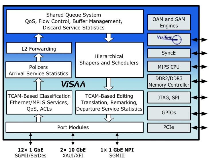
The Serval-2 architecture. Source: Vitesse
Vitesse Semiconductor has detailed its latest Carrier Ethernet access switch for mobile backhaul, cloud and enterprise services.
The Serval-2 chip broadens Vitesse's access switch offerings, adding 10 Gigabit Ethernet (GbE) ports while near-tripling the switching capacity to 32 Gigabit; the Serval-2 has 2x10 GbE and 12 1GbE ports.
The device features Vitesse's service aware architecture (ViSAA) that supports Carrier Ethernet 2.0 (CE 2.0). "We have built a hardware layer into the Ethernet itself which understands and can provision services," says Uday Mudoi, product marketing director at Vitesse.
CE 2.0, developed by the Metro Ethernet Forum (MEF), is designed to address evolving service requirements. First equipment supporting the technology was certified in January 2013. What CE 2.0 does not do is detail how services are implemented, says Mudoi. Such implementations are the work of the ITU, IETF and IEEE standard bodies with protocols such as Muti-Protocol Label Switching (MPLS)/ MPLS-Transport Profile (MPLS-TP) and provider bridging (Q-in-Q). "There is a full set of Carrier Ethernet networking protocols which comes on top of CE 2.0," says Mudoi.
Serval-2 switch
The Serval-2 switch features include 256 Ethernet virtual connections, hierarchical quality of service (QoS), provider bridging, and MPLS/ MPLS-TP.
An Ethernet Virtual Connection (EVC) is a logical representation of an Ethernet service, says Vitesse, a connection that an enterprise, data center or cell site uses to send traffic over the WAN.
Multiple EVCs can run on the same physical interface and can be point-to-point, point-to-multipoint, or multipoint-to-multipoint. Each EVC can have a bandwidth profile that specifies the committed information rate (CIR) and excess information rate (EIR) of the traffic transmitted to, or received from, the Ethernet service provider’s network.
The EVC also supports one or more classes of service and measurable QoS performance metrics. Such metrics include frame delay - latency - and frame loss to meet a particular application performance requirements.
The Serval-2 supports 256x8 class of service (CoS) EVCs, equivalent to over 4,000 bi-directional Ethernet services, says Mudoi.
The Serval-2 also supports per-EVC hierarchical queuing. It allows for 256 bi-directional EVCs with policing, statistics, and QoS guarantees for each CoS and EVC. Hierarchical QoS also enables a mix of any strict or byte-accurate weighting within the EVC, and supports the MEF's dual leaky bucket (DLB) algorithm that shapes traffic per-EVC and per-port.
"Service providers guarantee QoS to subscribers for the services that they buy," says Mudoi. "If each subscriber's traffic - even different applications per-subscriber - is treated using separate queues, then one subscriber's behavior does not impact the QoS of another." Supporting thousands of queues allows service providers to offer thousands of services, each with its own QoS.

Q-in-Q, defined in IEEE 802.1ad, allows for multiple VLAN headers - tags - to be inserted into a frame, says Mudoi, enabling service provider tags and customer tags.
Meanwhile, MPLS/ MPLS-TP direct data from one network node to the next based on shortest path labels rather than on long network addresses, thereby avoiding complex routing table look-ups. The labels identify virtual links between distant nodes rather than endpoints.
MPLS can encapsulate packets of various network protocols. Serval-2's MPLS-TP supports Label Edge Router (LER) with Ethernet pseudo-wires, Label Switch Router (LSR), and H-VPLS edge functions.
Q-in-Q in considered a basic networking function for enterprise and carrier networks, says Mudoi, while MPLS-TP is a more complex protocol.
Serval-2 also supports service activation and Vitesse's implementation of the IEEE 1588v2 timing standard, dubbed VeriTime.
"Before you provision a service, you need to run a test to make sure that once your service is provisioned, the user gets the required service level agreement," says Mudoi. Serval-2 supports the latest ITU-T Y.1564 service activation standard.
IEEE 1588v2 establishes accurate timing across a packet-based network and is used for such applications as mobile. The Serval-2 also benefits from Intellisec, Vitesse's MACsec Layer 2 security standard implementation (see Vitesse's Intellisec ).
"Both [Vitesse's VeriTime IEEE 1588v2 and Intellisec technologies] highly complement what we are doing in ViSAA," says Mudoi.
Availability
Serval-2 samples will be available in the third quarter of 2013. Vitesse expects it will take six months for system qualification such that Ethernet access devices using the chip and carrying live traffic are expected in the first half of 2014.
Netronome uses its network flow processor for OpenFlow
Part 2: Hardware for SDN
Netronome has demonstrated its flow processor chip implementing the OpenFlow protocol, an open standard implementation of software-defined networking (SDN).

"What OpenFlow does is let you control the hardware that is handling the traffic in the network. The value to the end customer is what they can do with that"
David Wells, Netronome
The reference design demonstration, which took place at an Open Networking User Group meeting, used the fabless semiconductor player's NFP-3240 network flow processor. The NFP-3240 was running the latest 1.3.0 version of the OpenFlow protocol.
Last year Netronome announced its next-generation flow processor family, the NFP-6xxx. The OpenFlow demonstration hints at what the newest flow processor will enable once first samples become available at the year end.
Netronome believes its flow processor architecture is well placed to tackle emerging intelligent networking applications such as SDN due to its emphasis on packet flows.
“In security, mobile and other spaces, increasingly there needs to be equipment in the network that is looking at content of packets and states of a flow - where you are looking at content across multiple packets - to figure out what is going on,” says David Wells, co-founder of Netronome and vice president of technology. “That is what we term flow processing."
This requires equipment able to process all the traffic on network links at 10 and 40 Gigabit-per-second (Gbps), and with next-generation equipment at 100Gbps. "This is where you do more than look at the packet header and make a switching decision," says Wells.
Software-defined networking
Operators and content service providers are interested in SDN due to its promise to deliver greater efficiencies and control in how they use their switches and routers in the data centre and network. With SDN, operators can add their own intelligence to tailor how traffic is routed in their networks.

In the data centre, a provider may be managing a huge number of servers running virtualised applications. "The management of the servers and applications is clever enough to optimise where it moves virtual machines and where it puts particular applications," says Wells. "You want to be able to optimise how the traffic flows through the network to get to those servers in the same way you are optimising the rest of the infrastructure."
Without OpenFlow, operators depend on routing protocols that come with existing switches and routers. "It works but it won't necessarily take the most efficient route through the network," says Wells.
OpenFlow lets operators orchestrate from the highest level of the infrastructure where applications reside, map the flows that go to them, determine their encapsulation and the capacity they have. "The service can be put in a tunnel, for example, and have resource allocated to it so that you know it is not going to be contended with," says Wells, guaranteeing services to customers.
"What OpenFlow does is let you control the hardware that is handling the traffic in the network," says Wells. "The value to the end customer is what they can do with that, in conjunction with other things they are doing."
Operators are also interested in using OpenFlow in the wide area network. "The attraction of OpenFlow is in the core and the edge [of the network] but it is the edge that is the starting point," says Wells.
OpenFlow demonstration
Netronome's OpenFlow demonstration used an NFP-3240 on a PCI Express (PCIe) card to run OpenFlow while other Netronome software runs on the host server in which the card resides.
The NFP-3240 classifies the traffic and implements the actions to be taken on the flows. The software on the host exposes the OpenFlow application programming interface (API) enabling the OpenFlow controller, the equipment that oversees how traffic is handled, to address the NFP device and influence how flows are processed.
Early OpenFlow implementations are based on Ethernet switch chips that interface to a CPU that provides the OpenFlow API. However, the Ethernet chips support the OpenFlow 1.1.0 specification and have limited-sized look-up tables with 98, 64k or 100k entries, says Wells.
The OpenFlow controller can write to the table and dictate how traffic is handled, but its size is limited. "That is a starting point and is useful," says Wells. "But to really do SDN, you need hardware platforms that can handle many more flows than these switches."
This is where the NFP processor is being targeted: it is programmable with capabilities driven by software rather than the hardware architecture, says Wells.
NFP-6xxx architecture
The NFP-6xxx is Netronome's latest network flow processor (NFP) family, rated at 40 to 200Gbps. No particular devices have yet been detailed but the highest-end NFP-6xxx device will comprise 216 processors: 120 flow processors (see chart - Netronome's sixth generation device) and new to its NFP devices, 96 packet processors.
The architecture is made up of 'islands', units that comprise a dozen flow processors. Netronome will combine different numbers of islands to create the various NFP-6xxx devices.
The input-output bandwidth of the device is 800Gbps while the on-chip memory totals 30 Megabyte. The device also interfaces directly to QSFP, SFP+ and CFP optical transceivers.
The 120 flow processors tackle the more complex, higher-layer tasks. Netronome has added packet processors to the NFP-6xxx to free the flow processors from tasks such as taking packets from the input stream and passing them on to where they are processed. The packet processors are programmable and perform such tasks as header classification before being processed by the flow processors.
The NFP-6xxx devices will include some 100 hardware accelerator engines for tasks such as traffic management, encryption and deep packet inspection.
The device will be implemented using Intel's latest 22nm 3D Tri-Gate CMOS process and is designed to work with high-end general purpose CPUs such as Intel's x86 devices, Broadcom's XLP and Freescale's PowerPC.
Markets
The data centre, where SDN is already being used, is one promising market for the device as customers look to enhance their existing capabilities.
There are requirements for intelligent gateways now but this is a market that is a year or two out, says Wells. Use of OpenFlow to control large IP core routers or core optical switches is a longer term application. "Those areas will come but it will be further out," says Wells.
For other markets such as security, there is a need for knowledge about the state of flows. This is more sophisticated treatment of packets than the simple looking up the action required based on a packet's header. Netronome believes that OpenFlow will develop to not only forward or terminate traffic at a certain destination but will also send traffic to a service before it is returned.
"You could insert a service in a OpenFlow environment and what it would do is guide packets to that service and return it but inside that service you may do something that is stateful," says Wells. This is just the sort of task security performs on flows. For example, an intrusion prevention system as a service or a firewall function. This function could be run on a dedicated platform or as a virtual application running on Netronome's flow processor.
Further reading:
Part 1: The role of software defined networking for telcos
EZchip expands the role of the network processor, click here
EZchip expands the role of the network processor
- EZchip's NPS-400 will be a 200Gbps duplex chip capable of layer 2 to layer 7 network processing
- The device is being aimed at edge routers and the data centre
- First samples by year end
EZchip Semiconductor has announced a class of network processor capable of performing traditional data plane processing as well as higher layer networking tasks. EZchip's announced NPS will extend the role of the network processor to encompass layer two to layer seven of the network. Source: EZchip
"It [the device family] is designed to provide processing for all the networking layers, from layer two all the way to layer seven," says Amir Eyal, EZchip’s vice president of business development. Network processors typically offer layer-two and layer-three processing only.
The device family, called the network processor for smart networks (NPS), is being aimed at Carrier Ethernet edge router platforms, the traditional telecom application for network processors.
But the NPS opens up new opportunities for EZchip in the data centre, such as security, load balancing and software-defined networking (SDN). Indeed EZchip says the NPS market will double the total addressable market to US$2.4bn by 2016.
"SDN is supposedly a big deal in the data centre," says Eyal. Because SDN separates the control plane from the data plane, it implies that the data plane becomes relatively simple. In practice the opposite is true: the data processing becomes more complex requiring the recognition and handling of packets having different encapsulation schemes, says Eyal.
The NPS borrows architectural elements of EZchip's existing high-end NPUs but the company has added an ARC 32-bit reduced instruction set computer (RISC) processor which it has redesigned to create the basic packet-processing computing node: the CTOP (C-programmable task-optimised processor).
EZchip has announced two NPS devices: The NPS-200 and the more processing-capable NPS-400. The NPS-400 is a 200 Gigabit-per-second (Gbps) duplex chip with 256 CTOPs, giving it twice the packet-processing performance of EZchip's latest NP-5 NPU. The NPS-400 will also have 800 Gigabit of input/ output. The NPS-200 design will have 128 CTOPs.
As a result of adding the ARC, the NPS family will be C-programmable whereas NPUs are programmed using assembly language or micro-code. The CTOP will also be able to processes 16 instruction threads whereas the standard ARC is single thread.
The NPS also features an on-chip traffic manager which controls the scheduling of traffic after it has been processed and classified.
The power consumption of the NPS has yet to be detailed but Eyal says it will be of the order of the NP-5 which is 60W.
EZchip says up to eight NPS chips could be put on a line card, to achieve a 1.6Tbps packet throughput, power-consumption permitting.
Adopting the NPS processor will eliminate the need to add to platforms service line cards that use general-purpose processors. More NPS-based cards can then be used in the vacated line-card slots to boost the platform's overall packet-processing performance.
The company started the NPS design two years ago and expects first samples at the end of 2013. NPS-based products are expected to be deployed in 2015.
Meanwhile, EZchip says it is sampling its NP-5 NPU this quarter. The NPS will overlap with the NP-5 and be available before the NP-6, the next NPU on EZchip's roadmap.
Will the NPS-400 with double the throughput not deter sales of the NP-5, even if the design is used solely for traditional NPU layer-two and layer-three tasks?
EZchip says new customers will likely adopt the NPS especially given its support for high-level programming. But existing customers using the NP-4 will prefer to stay with the NPU family due to the investment already made in software.
Further reading:
Microprocessor Report: EZchip breaks the NPU mold, click here
A Terabit network processor by 2015?, click here
Carrier Ethernet switch chip for wireless small cells
- 6-port low power 12 Gigabit Carrier Ethernet switch chip
- Used for intra and inter-board comms, and back-hauling
- Supports MPLS and MPLS-TP

"Multi-carrier OA&M performance monitoring allows you to manage your network for your users through another carrier’s network”
Uday Mudoi, Vitesse Semiconductor
Vitesse Semiconductor has launched an Ethernet switch chip for Long Term Evolution (LTE) small cells.
Small cells are being adopted by mobile operators as a complement to their existing macrocells to boost signal coverage and network capacity. The small cells include microcells and picocells as well as femtocells for the enterprise.
The Serval Lite chip, the VSC7416, from Vitesse will be used to aggregate and switch traffic and will reside at the interface between the access and the pre-aggregation segments of the mobile network.
According to Uday Mudoi, director of product marketing at Vitesse, two units make up a carrier’s small cell: the base station and the back-hauling. The base station itself comprises baseband and general purpose processing. “What we are seeing on a base station – whether it is a macro or a small cell – is the use of multi-core processors, and you may need more than one such device on the baseband card,” says Mudoi. The Serval Lite IC can be used as an interface between the baseband and general purpose processors, and to other hardware on the card.
 The basestation features baseband (BB) and general purpose processing (GPP) cards. Source: Vitesse
The backhaul unit also features the Serval Lite IC. “The backhaul is more interesting from a switch perspective,” says Mudoi. The switch takes traffic from the base stations and places it on the outgoing interface, typically a microwave or fibre link, says Mudoi.
The switch also supports Carrier Ethernet for the traffic back-hauling. Such features include hierarchical quality of service (QoS), performance monitoring and operations, administration and management (OA&M). "Multi-carrier OA&M performance monitoring allows you to manage your network for your users through another carrier’s network,” says Mudoi.
Switch characteristics
The Serval Lite is implemented using a 65nm CMOS process. The IC has six ports: four at 1 Gigabit Ethernet (GbE) and two that run at 1GbE or 2.5GbE. There is also a choice of NPI and PCI Express interfaces to connect to processors.
The chip has a full line rate switching capacity of 12 Gigabit. “It is a standard switching device, from any port to any port, that is standards compliant,” says Mudoi.
The switch supports the IEEE1588v2 timing protocol needed to synchronise between cell sites. The device also supports MPLS (Multiprotocol Label Switching) and MPLS-TP (Multiprotocol Label Switching Transport Profile).
“The 1588 timing issue is more complex when you are dealing with small cells,” says Mudoi. The back-hauling happens over millimeter wave or microwave links which adds extra timing constraints. This requires additional hardware to support the timing standard.
The device has been designed to achieve a low power consumption of typically 1.5W with the maximum being 3W. Vitesse has stripped out a T1/E1 processor used for back-hauling, with the chip supporting Ethernet only. The device also adheres to the IEEE 802.3az (Energy Efficient Ethernet), powering down the ports when inactive.
The switch features a single core 416 MHz MIPS processor used for overall management of the small cell. Samples of the VSC7416 are now available.
MultiPhy targets low-power coherent metro chip for 2013
MultiPhy has given first details of its planned 100 Gigabit coherent chip for metro networks. The Israeli fabless start-up expects to have samples of the device in 2013.

"We can tolerate greater [signal] impairments which means the requirements on the components we can use are more relaxed"
Avi Shabtai, CEO of MultiPhy
"Coherent metro is always something we have pushed," says Avi Shabtai, CEO of MultiPhy. Now, the company says it is starting to see a requirement for coherent technology's deployment in the metro. "Everyone expects to see it [coherent metro] in the next 2-3 years," he says. "Not tomorrow; it will take time to develop a solution to hit the target-specific [metro] market."
MultiPhy is at an advanced stage in the design of its coherent metro chip, dubbed the MP2100C. "It is going to be a very low power device," says Shabtai. MultiPhy is not quoting target figures but in an interview with the company's CTO, Dan Sadot, a figure of 15W was mentioned. The goal is to fit the design within a 24W CFP. This is a third of the power consumed by long-haul coherent solutions.
The design is being tackled from scratch. One way the start-up plans to reduce the power consumption is to use a one-sample-per-symbol data rate combined with the maximum-likelihood sequence estimation (MLSE) algorithm.
MultiPhy has developed patents that involve sub-Nyquist sampling. This allows the analogue-to-digital converters and the digital signal processor to operate at half the sampling rate, saving power. To use sub-Nyquist sampling, a low-pass anti-aliasing filter is applied but this harms the received signal. Using the filter, sampling at half the rate can occur and using the MLSE algorithm, the effects of the low-pass filtering can be countered. And because of the low-pass filtering, reduced bandwidth opto-electronics can be used which reduces cost.
This low-power approach is possible because the reach requirements in metro, up to 1,000km, is shorter than long haul/ ultra long haul optical transmission links. The shorter-reach requirements also impact the forward error correction codes, needed which can lessen the processing load, and the components, as mentioned. "We can tolerate greater [signal] impairments which means the requirements on the components we can use are more relaxed," says Shabtai.
The company also revealed that the MP2100C coherent device will integrate the transmitter and receiver on-chip.
MultiPhy says it is working with several system vendor and optical module partners on the IC development. Shabtai expects the first industry products using the chip to appear in 2014 or 2015. The timing will also be dependent on the cost and power consumption reductions of the accompanying optical components.
 A 100Gbps direct-detection optical module showing MultiPhy's multiplexer and receiver ICs. The module shown is a WDM design. Source: MultiPhy
100Gbps direct detection multiplexer chip
MultiPhy has also announced a multiplexer IC for 100 Gigabit direct detection. The start-up can now offer customers the MP1101Q, a 40nm CMOS multiplexer complement to its MP1100Q receiver IC that includes a digital signal processor to implements the MLSE algorithm. The MP1100Q was unveiled a year ago.
Testing the direct-detection chipset, MultiPhy says it can compensate +/-1000ps/nm of dispersion to achieve a point-to-point reach of 55km. No other available solution can meet such a reach, claims MultiPhy.
MultiPhy's direct-detection solution also enables 10 Gigabit-per-second (Gbps) opto-electronics components to be used for the transmit and receive paths. At ECOC, MultiPhy announced that it has used Sumitomo Electric's 10Gbps 1550nm externally-modulated lasers (EMLs) to demonstrate a 40km reach.
Using such 10Gbps devices simplifies the design since no 25Gbps components are required. It will also enable more optical module makers to enter the 100 Gigabit marketplace, claims MultiPhy. "It is twice the distance and about half of the cost of any other solution on the market - much below $10,000," says Shabtai.
 MultiPhy's HQ in Ness Ziona, Israel
The multiplexer device can also be used for traditional 4x28Gbps WDM solutions to achieve a reach in existing networks of up to 800km.
MultiPhy says that it expects the overall 100 Gigabit direct detection market to number 4 optical module makers and 4-5 system vendors by the end of 2012. At present ADVA Optical Networking is offering a 100Gbps direct-detection CFP-based design. ECI Telecom has detailed a 5x7-inch MSA direct-detection 100 Gigabit module, while Finisar and Oclaro have both announced that they are coming to market with 100Gbps direct-detection modules.
AppliedMicro samples 100Gbps CMOS multiplexer
AppliedMicro has announced the first CMOS merchant multiplexer chip for 100Gbps coherent optical transmission. The S28032 device supports dual polarisation, quadrature phase-shift keying (DP-QPSK) and has a power consumption of 4W, half that of current multiplexer chip designs implemented in BiCMOS.
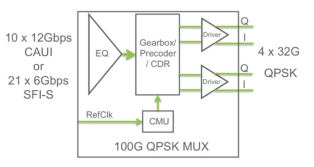 The S28032 100 Gig multiplexer IC. Source: AppliedMicro
"CMOS has a very low gain-bandwidth product, typically 100GHz," says Tim Warland, product marketing manager, connectivity solutions at AppliedMicro. “Running at 32GHz, we have been able to achieve a very high bandwidth with CMOS."
Significance
The availability of a CMOS merchant device will be welcome news for optical transport suppliers and 100Gbps coherent module makers. CMOS has better economics than BiCMOS due to the larger silicon wafers used and the chip yields achieved. The reduced power consumption also promotes the move to smaller-sized optical modules than the current 5x7-inch multi-source agreement (MSA).
"By reducing the power and the size, we can get to a 4x6-inch next-generation module,” says Warland. “And perhaps if we go for a shorter [optical transmission] reach - 400-600km - we could get into a CFP; then you can get four modules on a card.”
"Coherent ultimately is the solution people want to go to [in the metro] but optical duo-binary will do just fine for now"
Tim Warland, AppliedMicro
Chip details
The S28032 has a CAUI interface: 10x12Gbps input lanes that are multiplexed into four lanes at 28Gbps to 32Gbps. The particular data rate depends on the forward error correction (FEC) scheme used. The four lanes are DQPSK-precoded before being fed to the polarisation multiplexer to create the DP-QPSK waveforms.
The device also supports the SFI-S interface - 21 input channels, each at 6Gbps. This is significant as it enables the S28032 to be interfaced to NTT Electronics' (NEL) DSP-ASIC coherent receiver chip that has been adopted by 100Gbps module makers Oclaro and Opnext (now merged) as well as system vendors including Fujitsu Optical Systems and NEC.
 The mux IC within a 100Gbps coherent 5x7-inch optical module. Source: AppliedMicro
The AppliedMicro multiplexer IC, which is on the transmit path, interfaces with NEL's DSP-ASIC that is on the receiver path, because the FEC needs to be a closed loop to achieve the best efficiency, says Warland. "If you know what you are transmitting and receiving, you can improve the gain and modify the coherent receiver sampling points if you know what the transmit path looks like," he says.
The DSP-ASIC creates the transmission payloads and uses the S28032 to multiplex those into 28Gbps or greater speed signals.
The SFI-S interface is also suited to interface to FPGAs, for those system vendors that have their own custom FPGA-based FEC designs.
"Packet optical transport systems is more a potential growth engine as the OTN network evolves to become a real network like SONET used to be"
Francesco Caggioni. AppliedMicro
The multiplexer chip's particular lane rate is set by the strength of the FEC code used and its associated overhead. Using OTU4 frames with its 7% overhead FEC, the resulting data rate is 27.95Gbps. With a stronger 15% hard-decision FEC, each of the 4 channel's data rate is 30Gbps while it is 31.79Gbps with soft-decision FEC.
"It [the chip] has got sufficient headroom to accommodate everything that is available today and that we are considering in the OIF [Optical Internetworking Forum],” says Warland. The multiplexer is expected to be suitable for coherent designs that achieve a reach of up to 2,000-2,500km but the sweet spot is likely to be for metro networks with a reach of up to 1,000km, he says.
But while the CMOS device can achieve 32Gbps, it has its limitations. "For ultra long haul, we can't support a FEC rate higher than 20%," says Warland. "For that, a 25% to 30% FEC is needed."
AppliedMicro is sampling the device to lead customers and will start production in 1Q 2013.
What next
The S28032 joins AppliedMicro's existing S28010 IC suited for the 10km 100 Gigabit Ethernet 100GBASE-LR4 standard, and for optical duo-binary 100Gbps direct detection that has a reach of 200-1,000km.
"Our next step is to try and get a receiver to match this chip," says Warland. But it will be different to NEL's coherent receiver: "NEL's is long haul." Instead, AppliedMicro is eyeing the metro market where a smaller, less power-hungry chip is needed.
"Coherent ultimately is the solution people want to go to [in the metro] but optical duo-binary will do just fine for now," says Warland.
Two million 10Gbps OTN ports
AppliedMicro has also announced that it has shipped 2M 10Gbps OTN silicon ports. This comes 18 months after it announced that it had shipped its first million.
"OTN is showing similar growth to the 10 Gigabit Ethernet market but with a four-year lag," says Francesco Caggioni, strategic marketing director, connectivity solutions at AppliedMicro.
The company sees OTN growth in the IP edge router market and for transponder and muxponder designs, while packet optical transport systems (P-OTS) is an emerging market.
"Packet optical transport systems is more a potential growth engine as the OTN network evolves to become a real network like SONET used to be," says Caggioni. "We are seeing development but not a lot of deployment."
Further reading:
Cortina unveils multi-channel dispersion compensation chip
Cortina Systems has announced its latest electronic dispersion compensation (EDC) chip. The CS4342 is a compact device that supports eight duplex 10 Gigabit-per-second (Gbps) links.

"Some customers are doing 2,000 signals at 10 Gig across the backplane"
Scott Feller, Cortina
The chip is suited for use with optical modules and on line cards to counter the effect of transmission distortion where a bit's energy leaks into one or more adjacent bits, known as inter-symbol interference (ISI).
The Cortina device can be used for 10, 40 and 100Gbps line card and backplane designs and supports copper cable and optical fibre standards such as the multimode 10GBASE‐LRM and the 80km 10GBASE‐ZR interface.
Significance
Routeing high-speed signals from an ASIC to the various high-speed interfaces - 10Gbps and greater - is becoming harder as more interfaces are crammed onto a card.
"Boards are getting denser: from 48 ports to 96," says Scott Feller, director of the EDC product line at Cortina Systems. The issue with an ASIC on the board is that the distance it can span to the modules is only about 6-8 inches (~15-20cm). Placing the PHY chip on the board relaxes this constraint.
 The use of the octal EDC chip between a line card IC and SFP+ optical transceivers. Source: Cortina Systems
Vendors also gain greater flexibility in terms of the interfaces they can support. "These types of PHYs allow them [designers] to avoid having to make hard decisions," says Feller. "They put the PHY in front of the optical connector and they almost get every single optical format on the market."
The platforms using such EDC PHYs include data centre switches and telecom platforms such as packet optical transport systems (P-OTS). Data centre switches typically support Direct Attach Copper cable - a market area that has been growing significantly, says Cortina - and short-reach optical interfaces. For P-OTS the interfaces include the 10GBASE-ZR where EDC is a necessity.
The device is also being used for system backplanes where bandwidth requirements are increasing significantly. "Some customers are doing 2,000 signals at 10 Gig across the backplane," says Feller. "Now that there are so many signals - so much crosstalk - and the ASICs are further away from the backplane, so PHYs are starting to be put into systems."
 EDC employed in a backplane design. Source: Cortina Systems
Chip details
Cortina claims the 17x17 ball grid array CS4342 is a third smaller than competing devices. The chip compensates the received signal in the analogue domain. An on-chip DSP calculates the filter's weights to counter ISI while the filtering is performed using analogue circuitry. As a result, the EDC has a latency of 1ns only.
Cortina has dual, quad and now octal EDC ICs. It says that the delay between the different devices is the same such that both an octal and dual chip can be used to implement a 10-channel 100 Gig interface, for example the 10x10 MSA. In turn, future line cards supporting four 100Gbps interfaces would use five octal PHYs ICs.
The CS4342 is available in sample form and will enter production from October.
What next
"This type of product is at the very end of the food chain so there is always macro developments that could change the market," says Feller. Silicon photonics is one but Feller expects that it will be years before the technology is adopted widely in systems.
The external EDC PHYs must also compete with PHYs integrated within custom ASIC designs and FPGAs. "We always have to be ahead of the cost and performance curves on the PHY," says Feller. "If not, they [companies] are just going to integrate PHYs into their ASICs and FPGAs."
Meanwhile, Cortina says it has two more EDC devices in development.
A Terabit network processor by 2015?
Given that 100 Gigabit merchant silicon network processors will appear this year only, it sounds premature to discuss Terabit devices. But Alcatel-Lucent's latest core router family uses the 400 Gigabit FP3 packet-processing chipset, and one Terabit is the next obvious development.
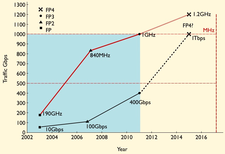 Source: Gazettabyte
Core routers achieved Terabit scale awhile back. Alcatel-Lucent's recently announced IP core router family includes the high-end 32 Terabit 7950 XRS-40, expected in the first half of 2013. The platform has 40 slots and will support up to 160, 100 Gigabit Ethernet interfaces.
Its FP3 400 Gigabit network processor chipset, announced in 2011, is already used in Alcatel-Lucent's edge routers but the 7950 is its first router platform family to exploit fully the chipset's capability.
The 7950 family comes with a selection of 10, 40 and 100 Gigabit Ethernet interfaces. Alcatel-Lucent has designed the router hardware such that the card-level control functions are separate from the Ethernet interfaces and FP3 chipset that both sit on the line card. The re-design is to preserve the service provider's investment. Carrier modules can be upgraded independently of the media line cards, the bulk of the line card investment.
The 7950 XRS-20 platform, in trials now, has 20 slots which take the interface modules - dubbed XMAs (media adapters) - that house the various Ethernet interface options and the FP3 chipset. What Alcatel-Lucent calls the card-level control complex is the carrier module (XCM), of which there are up to are 10 in the system. The XCM, which includes control processing, interfaces to the router's system fabric and holds up to two XMAs.
There are two XCM types used with the 7950 family router members. The 800 Gigabit-per-second (Gbps) XCM supports a pair of 400Gbps XMAs or 200Gbps XMAs, while the 400Gbps XCM supports a single 400Gbps XMA or a pair of 200Gbps XMAs.
The slots that host the XCMs can scale to 2 Terabits, suggesting that the platforms are already designed with the next packet processor architecture in mind.
FP3 chipset
The FP3 chipset, like the previous generation 100Gbps FP2, comprises three devices: the P-chip network processor, a Q-chip traffic manager and the T-chip that interfaces to the router fabric.
The P-chip inspects packets and performs the look ups that determine where the packets should be forwarded. The P-chip determines a packet's class and the quality of service it requires and tells the Q-chip traffic manager in which queue the packet is to be placed. The Q-chip handles the packet flows and makes decisions as to how packets should be dealt with, especially when congestion occurs.
The basic metrics of the 100Gbps FP2 P-chip is that it is clocked at 840GHz and has 112 micro-coded programmable cores, arranged as 16 rows by 7 columns. To scale to 400Gbps, the FP3 P-chip is clocked at 1GHz (x1.2) and has 288 cores arranged as a 32x9 matrix (x2.6). The cores in the FP3 have also been re-architected such that two instructions can be executed per clock cycle. However this achieves a 30-35% performance enhancement rather than 2x since there are data dependencies and it is not always possible to execute instructions in parallel. Collectively the FP3 enhancements provide the needed 4x improvement to achieve 400Gbps packet processing performance.
The FP3's traffic manager Q-chip retains the FP2's four RISC cores but the instruction set has been enhanced and the cores are now clocked at 900GHz.
Terabit packet processing
Alcatel-Lucent has kept the same line card configuration of using two P-chips with each Q-chip. The second P-chip is viewed as an inexpensive way to add spare processing in case operators need to support more complex service mixes in future. However, it is rare that in the example of the FP2-based line card, the capability of the second P-chip has been used, says Alcatel-Lucent.
Having the second P-chip certainly boosts the overall packet processing on the line card but at some point Alcatel-Lucent will develop the FP4 and the next obvious speed hike is 1 Terabit.
Moving to a 28nm or an even more advanced CMOS process will enable the clock speed of the P-chip to be increased but probably not by much. A 1.2GHz clock would still require a further more-than-doubling of the cores, assuming Alcatel-Lucent doesn't also boost processing performance elswhere to achieve the overall 2.5x speed-up to a 1 Terabit FP4.
However, there are two obvious hurdles to be overcome to achieve a Terabit network processor: electrical interface speeds and memory.
Alcatel-Lucent settled on 10Gbps SERDES to carry traffic between the chips and for the interfaces on the T-chip, believing the technology the most viable and sufficiently mature when the design was undertaken. A Terabit FP4 will likely adopt 25Gbps interfaces to provide the required 2.5x I/O boost.
Another even more significant challenge is the memory speed improvement needed for the look up tables and for packet buffering. Alcatel-Lucent worked with the leading memory vendors when designing the FP3 and will do the same for its next-generation design.
Alcatel-Lucent, not surprisingly, will not comment on devices it has yet to announce. But the company did say that none of the identified design challenges for the next chipset are insurmountable.
Further reading:
Network processors to support multiple 100 Gigabit flows
A more detailed look at the FP3 in New Electronics, click here
OTN processors from the core to the network edge
The latest silicon design announcements from PMC and AppliedMicro reflect the ongoing network evolution of the Optical Transport Network (OTN) protocol.

"There is a clear march from carriers, led in particular by China, to adopt OTN in the metro"
Scott Wakelin, PMC
The OTN standard, defined by the telecom standards body of the International Telecommunication Union (ITU-T), has existed for a decade but only recently has it emerged as a key networking technology.
OTN's growing importance is due to the enhanced features being added to the protocol coupled with developments in the network. In particular, OTN enhances capabilities that operators have long been used to with SONET/SDH, while also supporting packet-based traffic. Moreover chip vendors are unveiling OTN designs that now span the core to the network edge.
"OTN switching is a foundational technology in the network"
Michael Adams, Ciena
OTN supports 1 Gigabit Ethernet (GbE) with ODU0 framing alongside ODU1 (2.5G), ODU2 (10G), ODU3 (40G) and ODU4 (100G). The standard packs efficiently client signals such as SONET/SDH, Ethernet, video and Fibre Channel, at the various speed increments up to 100Gbps prior to transmission over lightpaths. Meanwhile, the Optical Internetworking Forum (OIF) has recently developed the OTN-over-Packet-Fabric standard that allows OTN to be switched using packet fabrics.
"OTN switching is a foundational technology in the network," says Michael Adams, Ciena’s vice president of product & technology marketing.
Operator benefits
Whereas 10Gbps services matched 10Gbps lightpaths only a few years ago, transport speeds have now surged ahead. Common services are at 1 and 10 GbE while transport is now at 40Gbps and 100Gbps speeds. OTN switching allows client signals to be combined efficiently to fill the higher capacity lightpaths and avoid stranded bandwidth in the network.
OTN also benefits network connectivity changes. With AT&T's Optical Mesh Service, for example, customers buy a total capacity and, using a web portal, can adapt connectivity between their sites as requirements change. "It [OTN] can manage GbE streams and switch them through the network in an efficient manner," says Adams.
The ability to adapt connectivity is also an important requirement for cloud computing, with OTN switching and a mesh control plane seen as a promising way to enable dynamic networking that provides guaranteed bandwidth when needed, says Ciena.
OTN also offers an alternative to IP-over-DWDM, argues Ciena. By adding a 100Gbps wavelength, service routers can exploit OTN to add 10G services as needed rather than keep adding a 10Gbps wavelength for each service using IP-over-DWDM. "To enable service creation quickly, why not put your router network on top of that network versus running it directly?" says Adams.
OTN hardware announcements
The latest OTN chip announcements from PMC and Applied Micro offer enhanced capacity when aggregating and switching client signals, while also supporting the interfacing to various switch fabrics.
PMC has announced two metro OTN processors, dubbed the HyPHY 20Gflex and 10Gflex. The devices are targeted at compact "pizza boxes" that aggregate residential, enterprise and mobile backhaul traffic, as well as packet-optical and optical transport platforms.
AppliedMicro's TPACK unit has unveiled two additions to its OTN designs: a 100Gbps chipset and the TPO134. The company also announced the general availability of its 100Gbps muxponder and transponder OTN design, now being deployed in the network.
 Source: AppliedMicro
"OTN has long had a home in the core of the network," says Scott Wakelin, product manager for HyPHY flex at PMC. "But there is a clear march from carriers, led in particular by China, to adopt OTN in the metro, whether layer-zero or layer-one switched."
Using various market research forecasts, PMC expects the global OTN chip market to reach US $600 million in 2015, the bulk being metro.
PMC and AppliedMicro offer application-specific standard product (ASSP) OTN ICs while AppliedMicro also offers FPGA-based OTN designs.
The benefits of using an FPGA, says AppliedMicro, include time-to-market, the ability to reprogramme the design to accommodate standards’ tweaks, and enabling system vendors to add custom logic elements to differentiate their designs. PMC develops ASSPs only, arguing that such chips offer superior integration, power efficiency and price points.
Both companies, when developing an ASSP, know that the resulting design will be adopted by end customers. When PMC announced its original HyPhy family of devices, seven of the top nine OEMs were developing board designs based on the chip family.
PMC's metro OTN processors
The HyPHY 20Gflex has 16 SFP (up to 5Gbps) and two 10Gbps XFP/SFP+ interfaces, whose streams it can groom using the device's 100Gbps cross-connect. The cross-connect can manipulate streams down to SONET/SDH STS-1/ STM-0 rates and ODU0 (1GbE) OTN channels.
Both ODU0 and ODUflex channels are supported. Before adding ODU0, a Gigabit Ethernet channel could only sit in a 2.5Gbps (ODU1) container, which wastes half the capacity. Similarly by supporting ODUflex, signals such as video can be mapped into frames made up of increments of 1.25Gbps. "For efficient use of resources from the metro into the core, you need to start at the access," said Wakelin.
 Source: PMC
The chip also supports the OTN-over-Packet-Fabric protocol. The devices can interface to OTN, SONET/SDH and packet switch fabrics.
The 20Gflex offers 40Gbps of OTN framing and a further 20Gbps of OTN mapping. The OTN mapping is used for those client signals to be fitted into ODU frames. With the additional 40Gbps interfaces that connect to the switch fabric, the total interface throughput is 100Gbps, matching the device's cross-connect capacity.
Other chip features include Fast Ethernet, Gigabit Ethernet and 10GbE MACs for carrier Ethernet transport, and support for timing over packet standards, including IEEE 1588v2 over OTN, used to carry mobile backhaul timing information.
The 10Gflex variant has similar functionality to the 20Gflex but with lower throughput.
PMC is now sampling the HyPHY Gflex devices to lead customers.
AppliedMicro's OTN designs
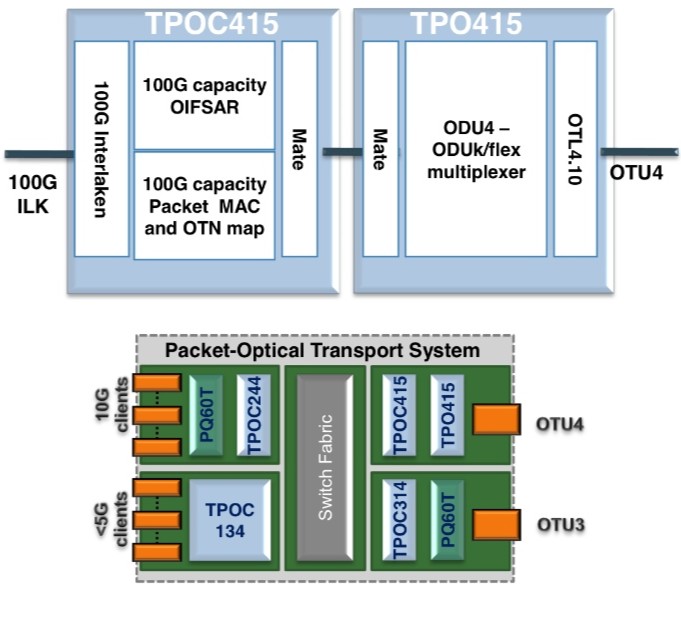
AppliedMicro's TPACK unit has unveiled two OTN designs: a TPO415/C415 OTN multiplexer chipset for use in 100Gbps packet optical transport line cards, and the TPO134 device used at the network edge.
The two devices combined - the TPO415 and TPOC415 - are implemented using FPGAs, what AppliedMicro dubs softsilicon. The two devices interface between the 100Gbps line side and the switch fabric. The TPO415 takes the OTU4 line side OTN signal and demultiplexes it to the various channel constituents. These can be ODU0, ODU1, ODU2, ODU3, ODU4 and ODUflex - capacity from 1Gbps to 100Gbps.

"The [100Gbps muxponder] design comes with an API that makes it look like one component"
Lars Pedersen, AppliedMicro
The TPOC415 has a 100Gbps, 80-channel segmentation and reassembly function (SAR) compliant with the OIF OTN-over-Packet-Fabric standard. The TPOC415 also has a 100Gbps, 80 channel packet mapper function for the transport of Ethernet and MPLS-TP over ODUk or ODUflex. The device's 100Gbps Interlaken interface is used to connect to the switch fabric for packet switching and ODU cross-connection. The devices can also be used in a standalone fashion for designs where the switch fabric does not use Interlaken, or when working with integrated switches and network processors.
 Source: AppliedMicro
"This is the first solution in the market for doing these hybrid functions at 100Gbps," says Lars Pedersen, CTO of AppliedMicro's TPACK.
The second design is the softsilicon TPO134, a 10Gbps add/drop multiplexer that can take in up to 16 clients signals and has two OTU2 interfaces. In between is the cross-connect that supports ODU0, ODU1 and ODUflex channels. Two devices can be combined to support 32 client channels and four OTU2 interfaces. Such a dual-design in a pizza-box system would be used to combine multiple client streams.
Being softsilicon, the TPO134 can also be used for packet optical transport systems. Here by downloading a different FPGA image, the design can also implement the segmentation and reassembly function required for the OIF's OTN-over-Packet-Fabric standard. "The interface to the switch fabric is Interlaken again," says Pedersen.
The TPO134 design doubles the capacity of AppliedMicro's previous add/drop multiplexer designs and is the first to support the OIF standard.
AppliedMicro has also announced the general availability of its 100G muxponder design. The muxponder design is a three-device chipset based on two PQ60 ASSPs and a TPO404 softsilicon design.
The PQ60T devices map 10 and 40Gbps clients into OTN and the TPO404 performs the multiplexing to OTU4 with forward error correction. The client signals supported include SONET/SDH, Ethernet and Fibre Channel. On the line side the design also supports various FEC schemes including an enhanced FEC. The TPO404 differ from the TPOT414/424 devices that link 100GbE and 100Gbps line side.
"The [100Gbps muxponder] design comes with an API [application programming interface] that makes it look [from a software perspective] like one component with some client and line ports, similar to the TPO134 device," says Pedersen.
Further reading:
Transport processors now at 100 Gigabit