

The era of cloud-scale routeing
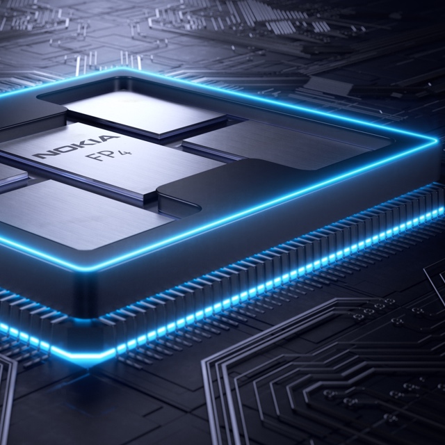 Nokia's FP4 p-chip. The multi-chip module shows five packages: the p-chip die surrounded by four memory stacks. Each stack has five memory die. The p-chip and memory stacks are interconnected using an interposer.
 - Nokia has unveiled the FP4, a 2.4 terabit-per-second network processor that has 6x the throughput of its existing FP3.
- The FP4 is a four-IC chipset implemented using 16nm CMOS FinFET technology. Two of the four devices in the chipset are multi-chip modules.
- The FP4 uses 56 gigabit-per-second serial-deserialiser (serdes) technology from Broadcom, implemented using PAM-4 modulation. It also supports terabit flows.
- Nokia announced IP edge and core router platforms that will use the FP4, the largest configuration being a 0.58 petabit switching capacity router.
Much can happen in an internet minute. In that time, 4.1 million YouTube videos are viewed, compared to 2.8 million views a minute only last year. Meanwhile, new internet uses continue to emerge. Take voice-activated devices, for example. Amazon ships 50 of its Echo devices every minute, almost one a second.
Given all that happens each minute, predicting where the internet will be in a decade’s time is challenging. But that is the task Alcatel-Lucent’s (now Nokia’s) chip designers set themselves in 2011 after the launch of its FP3 network processor chipset that powers its IP-router platforms.
Six years on and its successor - the FP4 - has just been announced. The FP4 is the industry’s first multi-terabit network processor that will be the mainstay of Nokia’s IP router platforms for years to come.
Cloud-scale routing
At the FP4’s launch, Nokia’s CEO, Rajeev Suri, discussed the ‘next chapter’ of the internet that includes smart cities, new higher-definition video formats and the growing number of connected devices.
IP traffic is growing at a compound annual growth rate (CAGR) of 25 percent through to 2022, according to Nokia Bell Labs, while peak data rates are growing at a 39 percent CAGR. Nokia Bell Labs also forecasts that the number of connected devices will grow from 12 billion this year to 100 billion by 2025.
Basil Alwan, Nokia’s president of IP and optical networks, said the internet has entered the era of cloud-scale routeing. When delivering a cloud service, rarely is the request fulfilled by one data centre. Rather, several data centres are involved in fulfilling the tasks. “One transaction to the cloud is multiplied,” said Alwan.
IP traffic is also becoming more dynamic, while the Internet of Things presents a massive security challenge.
Alwan also mentioned how internet content providers have much greater visibility into their traffic whereas the telcos’ view of what flows in their networks is limited. Hence their interest in analytics to understand and manage their networks better.
These are the trends that influenced the design of the FP4.
We put a big emphasis on making sure we had a high degree of telemetry coming out at the chip level
FP4 goals
Telemetry, the sending of measurement data for monitoring purposes, and network security were two key design goals for the FP4.
 Steve Vogelsang“We put a big emphasis on making sure we had a high degree of telemetry coming out at the chip level,” said Steve Vogelsang, CTO for Nokia's IP and optical business.
Tasks include counters, collecting statistics and packet copying. “This is to make sure we have the instrumentation coming off these systems that we can use to drive the [network] analytics platform,” said Vogelsang.
Being able to see the applications flowing in the network benefits security. Distributed Denial-of-Service (DDoS) attacks are handled by diverting traffic to a ‘scrubbing centre’ where sophisticated equipment separates legitimate IP packets from attack traffic that needs scrubbing.
The FP4 supports the deeper inspection of packets. “Once we identify a threat, we can scrub that traffic directly in the network,” said Vogelsang. Nokia claims that that the FP4 can deal with over 90 percent of the traffic that would normally go to a scrubbing centre.
Chipset architecture
Nokia’s current FP3 network processor chipset comprises three devices: the p-chip network processor, the q-chip traffic manager and the t-chip fabric interface device.
The p-chip network processor inspects packets and performs table look-ups using fast-access memory to determine where packets should be forwarded. The q-chip is the traffic manager that oversees the packet flows and decides how packets should be dealt with, especially when congestion occurs. The third FP3 chip is the t-chip that interfaces to the router fabric.
The FP4 retains the three chips and adds a fourth: the e-chip - a media access controller (MAC) that parcels data from the router’s client-side pluggable optical modules for the p-chip. However, while the FP4 retains the same nomenclature for the chips as the FP3, the CMOS process, chip architecture and packaging used to implement the FP4 are significantly more advanced.
The FP4 can deal with over 90 percent of the traffic that would normally go to a scrubbing centre
Nokia is not providing much detail regarding FP4 chipset's architecture, unlike the launch of the FP3. “We wanted to focus on the re-architecture we have gone through,” said Vogelsang. But looking at the FP3 design, insight can be gained as to how the FP4 has likely changed.
The FP3’s p-chip uses 288 programmable cores. Each programmable core can process two instructions each clock cycle and is clocked at 1GHz.
The 288 cores are arranged as a 32-row-by-9-column array. Each row of cores can be viewed as a packet-processing pipeline. A row pipeline can also be segmented to perform independent tasks. The array’s columns are associated with table look-ups. The resulting FP3 p-chip is a 400-gigabit network processor.
Vogelsang said there is limited scope to increase the clock speed of the FP4 p-chip beyond 1GHz. Accordingly, the bulk of the FP4’s sixfold throughput improvement is the result of a combination of programmable core enhancements, possible a larger core array and, most importantly, system improvements. In particular, the memory architecture is now packaged within the p-chip for fast look-ups, while the chipset’s input-output lanes have been boosted from 10 gigabits-per-second (Gbps) to 50Gbps.
Nokia has sought to reuse as much of the existing microcode to program the cores for the FP4 p-chip but has added new instructions to take advantage of changes in the pipeline.
Software compatibility already exists at the router operating system level. The same SROS router operating system runs on Nokia’s network processors, merchant hardware from the like of Broadcom and on x86 instruction-set microprocessors in servers using virtualisation technology.
Such compatibility is achieved using a hardware abstraction layer that sits between the operating system and the underlying hardware. “The majority of the software we write has no idea what the underlying hardware is,” said Vogelsang.
Nokia has a small team of software engineers focussed on the FP4’s microcode changes but, due to the hardware abstraction layer, such changes are transparent to the main software developers.
The FP3’s traffic manager, the q-chip, comprises four reduced instruction set computer (RISC) cores clocked at 900MHz. This too has been scaled up for the FP4 but Nokia has not given details.
The t-chip interfaces to the switch fabric that sits on a separate card. In previous generations of router products, a mid-plane is used, said Nokia. This has been scrapped with the new router products being announced. Instead, the switch cards are held horizontally in the chassis and the line cards are vertical. “A bunch of metal guides are used to guide the two cards and they directly connect to each other,” said Vogelsang. “The t-chips are what interface to these connectors inside the system.”
The MAC e-chip interfaces to the line card’s pluggable modules and support up to a terabit flow. Indeed, the MAC will support integer multiples of 100 Gigabit Ethernet from 100 gigabit to 1 terabit. Nokia has a pre-standard implementation of FlexMAC that allows it to combine lanes across multiple transceivers into a single interface.
Nokia will have line cards that support 24 or 36 QSFP-DD pluggable modules, with each module able to support 400 Gigabit Ethernet.
The FP4 is also twice as power efficient, consuming 4 gigabit/W.
We wanted to make sure we used a high-volume chip-packaging technology that was being driven by other industries and we found that in the gaming industry
Design choices
One significance difference between the two network processor generations is the CMOS process used. Nokia skipped 28nm and 22nm CMOS nodes to go from 40nm CMOS for the FP3 to 16nm FinFET for the FP4. “We looked at that and we did not see all the technologies we would need coming together to get the step-function in performance that we wanted,” said Vogelsang.
Nokia also designed its own memory for the FP4.
“A challenge we face with each generation of network processor is finding memories and memory suppliers that can offer the performance we need,” said Vogelsang. The memory Nokia designed is described as intelligent: instructions can effectively be implemented during memory access and the memory can be allocated to do different types of look-up and buffering, depending on requirements.
Another key area associated with maximising the performance of the memory is the packaging. Nokia has adopted multi-chip module technology for the p-chip and the q-chip.
“We wanted to make sure we used a high-volume chip-packaging technology that was being driven by other industries and we found that in the gaming industry,” said Vogelsang, pointing out that the graphics processing unit (GPU) has similar requirements to those of a network processor. GPUs are highly memory intensive while manipulating bits on a screen is similar to manipulating headers and packets.
The resulting 2.5D packaged p-chip comprises the packet processor die and stacks of memory. Each memory stack comprises 5 memory die. All sit on an interposer substrate - itself a die that is used for dense interconnect of devices. The resulting FP4 p-chip is thus a 22-die multi-chip module.
“Our memory stacks are connected at the die edges and do not use through-silicon vias,” said Vogelsang. “Hence it is technically a 2.5D package [rather than 3D].”
The q-chip is also implemented as a multi-chip module containing RISC processors and buffering memory, whereas the router fabric t-chip and MAC e-chip are single-die ICs.
The FP4’s more advanced CMOS process also enables significantly faster interfaces. The FP4 uses PAM-4 modulation to implement 56Gbps interfaces. “You really need to run those bit rates much much higher to get the traffic into and out of the chip,” said Vogelsang.
Nokia says it is using embedded serialiser-deserialiser interface technology from Broadcom.
Next-gen routers
Nokia has also detailed the IP edge and core routers that will use the FP4 network processor.
The 7750 Service Router (SR-s) edge router family will support up to 144 terabits in a single shelf. This highest capacity configuration is the 7750 SR-14. It is a 24-rack-unit-plus-the-power-supply high chassis and supports a dozen line cards, each 12Tbps when using 100-gigabit modules, or 24x400GbE when using QSFP-DD modules.
Another new platform is the huge 7950 Extensible Routing System (XRS-XC) IP core router which can be scaled to 576 terabits - over half a petabit - when used in a six-chassis configuration. Combining the six chassis does not make require the use of front-panel client-side interfaces. Instead, dedicated interfaces are used with active optical cables to interlink the chassis.
The first router products will be shipped to customers at the year end with general availability expected from the first quarter of 2018.

Creating a long-term view for the semiconductor industry
The semiconductor industry is set for considerable change over the next 15 years.
“We are at an inflection point in the history of the [chip] industry,” says Thomas Conte, an IEEE Fellow. “It will be very different and very diverse; there won’t be one semiconductor industry.”
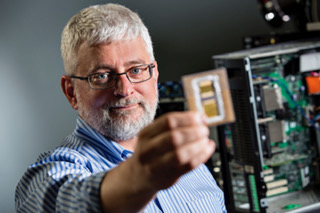
Conte (pictured) is co-chair of the IEEE Rebooting Computing initiative that is sponsoring the International Roadmap of Devices and Systems (IRDS) programme (See The emergence of the IRDS, below). The IRDS is defining technology roadmaps over a 15-year horizon and in November will publish its first that spans nine focus areas.
The focus of the IRDS on systems and devices and the broadening of technologies being considered is a consequence of the changing dynamics of the chip industry.
Conte stresses that it is not so much the ending of Moore’s Law that is causing the change as the ending of CMOS. Transistors will still continue to shrink even though it is becoming harder and costlier to achieve but the scaling benefits that for decades delivered a constant power density for chips with each new CMOS process node ended a decade ago.
“Back in the day it was pretty easy to plot it [the roadmap] because the technology was rather static in what we wanted to achieve,” says Conte. That ‘cushy ride’ that CMOS has delivered is ending. “The question now is: Are there other technologies we should be investing in that help applications move forward?” says Conte.
Focus groups
The IRDS has set up nine focus groups and in March published the first white papers from the teams.
The most complete white paper is from the More Moore focus group which looks at how new generations of smaller transistor features will be achieved. “It is clear that for the next 10 to 15 years we still have a lot of CMOS nodes left,” says Conte. “We still have to track what happens to CMOS.”
Conte says it is becoming clearer that ICs, in general, are going to follow the course of flash memory and be constructed as 3D monolithic designs. “We are just beginning to understand how to do this," says Conte.
"This does not mean we are going to get transistors that make computing faster without doing something different,” he says. This explains the work of the Beyond CMOS (Emerging Research Devices) focus team that is looking at alternative non-CMOS technologies to advance systems performance.
It is clear that for the next 10 to 15 years we still have a lot of CMOS nodes left
A third IRDS focus group is Outside System Connectivity which includes interface technologies such as photonic interconnect needed for future systems. “Outside System Interconnect is an important focus group and it is also our interface to the IEEE 5G roadmap team,” he says.
Conte also highlights two other IRDS focus teams: System and Architecture, and Applications Benchmarking. “These two focus teams are really important as to what the IRDS is all about,” says Conte.
The System and Architecture group has identified four systems views that it will focus on: the data centre, mobile handsets and tablets, edge devices for the Internet of Things, and control systems for the cyber-physical world such as automation, robotics and automotive systems.
The Application Benchmarking focus group is tasked with predicting key applications, quantifying how their performance is evolving and identifying roadblocks that could hinder their progress. Feature recognition, an important machine learning task, is one such example.
The IRDS is also continuing the working format established by the ITRS whereby every odd year a new 15-year roadmap is published while updates are published every even year.
Roadmapping
Three communities contribute to the development of the IRDS roadmap: industry, government and academia.
Industry is more concerned with solving their immediate problems and do not have the time or resources to investigate something that might or might not work in 15 years’ time, says Conte. Academia, in contrast, is more interested in addressing challenging problems over a longer term, 15-year horizon. Government national labs in the US and Europe’s imec sit somewhere in between and try to come up with mid-range solutions. “It is an interesting tension and it seems to work,” says Conte.
Contributors to the IRDS are from the US, Europe, Japan, South Korea and Taiwan but not China which is putting huge effort to be self-sufficient in semiconductors.
“We have not got participation for China yet,” says Conte. “It is not that we are against that, we just have not made the connections yet.” Conte believes China’s input would be very good for the roadmap effort. “They are being very aggressive and bright and they are more willing to take risks than the West,” he says.
What will be deemed a success for the IRDS work?
“It is to come up with a good prediction that is 15 years out and identify what the roadblocks are to getting there.”
____________________________________________________________
The emergence of the IRDS
The IRDS was established in 2016 by the IEEE after it took over the roadmap work of the International Technology Roadmap for Semiconductors (ITRS), an organisation sponsored by the five leading chip manufacturing regions in the world.
“The [work of the] ITRS was a bottoms-up roadmap, driven by the semiconductor industry,” says Conte. “It started with devices and didn't really go much higher.”
With the end of scaling, whereby the power density of chips remained constant with each new CMOS process node, the ITRS realised its long-established roadmap work needed a rethink which resulted in the establishment of ITRS 2.0.
“The ITRS 2.0 was an attempt to do a top-down approach looking at the system level and working down to devices,” says Conte. It was well received by everyone but the sponsors, says Conte, which was not surprising given their bottoms-up focus. It resulted in the sponsors of the ITRS 2.0 such as the US Semiconductor Industry Association (SIA) pulling out and the IEEE stepping in.
“This is much closer to what we are trying to do with the Rebooting Computing so it makes sense this group comes into the IEEE band and we act as a sponsor,” says Conte.
DIMENSION tackles silicon photonics’ laser shortfall
Several companies and research institutes, part of a European project, are developing a silicon photonics process that combines on-chip electronics and lasers. Dubbed Dimension (Directly Modulated Lasers on Silicon), the silicon photonics project is part of the European Commission’s Horizon 2020 research and innovation programme.
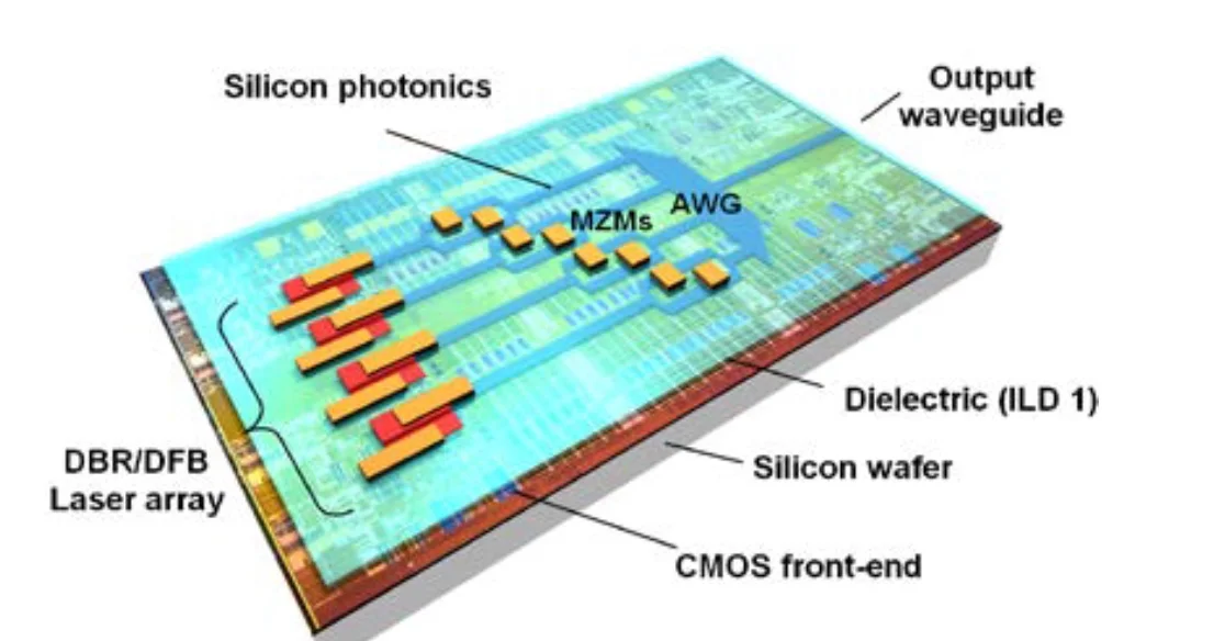 The Dimension process showing the passive photonics, dielectric material, BiCMOS circuitry, and the on-chip lasers and modulators. The indium phosphide material is shown in red. Source: Dimension.
Goal
Silicon photonics has long been seen as a technology having the potential to deliver optical devices at CMOS manufacturing costs. But silicon's key shortfall is that it does not lase. “What we see with today’s solutions is a very low-cost chip with a lot of functionality, which is a great thing, but in addition you need lasers,” says Bert Offrein, principal research staff member and manager of neuromorphic devices and systems at IBM Research, a participant in the Dimension project.
The laser accounts for a relatively large fraction of the total bill of materials of a silicon photonics chip. In turn, connecting the light source to the chip is not trivial and adds to the packaging costs. “In this project, we try to tackle this [laser] issue,” says Offrein.
The project's goal is to develop manufacturing processes that will enable the integration of photonics, including the laser, and electronics, all on one chip. “By fully integrating the laser on the chip, we massively reduce the cost and create additional functionality,” says Offrein.
“This is the true embodiment of what people first pictured as silicon photonics: the combination of optics and electronics on a single chip,” says Lars Zimmermann, team leader, silicon photonics at the Innovations for High Performance Microelectronics (IHP) research institute, another member of Dimension.
Proof-of-concept demonstrators
Dimension is a four-year project that will end in early 2020. Other project participants besides IBM Research and the IHP include ADVA Optical Networking, Opticap and the Athens Information Technology (AIT) research centre. The Dresden University of Technology is overseeing the project.
The project has set itself the goal of producing three proof-of-concept designs using the integrated silicon photonics technology.
One is a 400 Gigabit Ethernet (GbE) transmitter made up of eight 50 gigabit-per-second (Gbps) channels, each comprising a 25 gigabaud directly-modulated laser combined with 4-level pulse amplitude modulation (PAM4). Two variants are planned: a directly modulated version for the 400GbE 2km reach specification, and one with external modulation for the 400GbE 10km reach standard.
Another design is a coherent transmitter for such applications as data centre interconnect, compromising a monolithically integrated narrow-linewidth tunable laser, modulator and driver. The coherent transmitter will have a 10km target reach, will operate at 25Gbps and have a tunable narrow linewidth of under 1MHz.
The third, final demonstrator is a directly-modulated 25-gigabit non-return-to-zero laser using indium phosphide grown directly on the silicon.
By fully integrating the laser on the chip, we massively reduce the cost and create additional functionality
Process details
The silicon photonics manufacturing process involves using a silicon-on-insulator (SOI) wafer to implement the passive photonics functions and the electronics. The electronics supports high-speed analogue driver transistors and a 0.25-micron BiCMOS process used to implement the chip's control logic and control interfaces.
 Bert Offrein
The laser is constructed by first bonding a thin layer of indium phosphide. “It is structured in such a way that it [the III-V material] can be embedded completely in the whole CMOS processing,” says Offrein.
The indium phosphide layer, referred to as a III-V membrane, sits on a thin dielectric layer placed on the SOI wafer. The dielectric material is needed to protect the wafer from contamination by the III-V material and ensure that such a design could be manufactured in a BiCMOS foundry.
Once the thin indium phosphide layer is deposited, the laser can be constructed. The final stages, part of the chip-making back-end process, is the adding of metallisation layers that connect the laser and the electronics, and the circuits to the interface signals.
Growing lasers on silicon
Growing the indium phosphide layer directly on silicon, as will be done for the third demonstrator, is more exploratory. “We want to show there is a path forward on this III-V-on-silicon technology to reduce the cost further,” says Offrein.
 Lars Zimmermann
The challenge growing indium phosphide on silicon is the lattice mismatch that occurs between the two materials which leads to defects.
To tackle the issue, an approach known as confined growth is used. A small ‘seed’ is put on the silicon to act as a growth point for the indium phosphide. A small cavity is created using silica to confine the resulting growth. “The material grows in this glass cavity and the defects grow out and disappear at the edges,” says Offrein. “You then have a very high-quality III-V in this glass and this is the starting point to continue to build the quantum wells that we need.”
One challenge is enlarging the confined growth area. So far, such growth is limited to a micron whereas the length of a laser can be 500 microns typically. And once the laser is built, there remain the issues of laser reliability and temperature stability. “We will see challenges but we are not there yet,” says Offrein.
This is the true embodiment of what people first pictured as silicon photonics: the combination of optics and electronics on a single chip
Status
Dimension is tackling designs for communications but such on-chip lasers will also be useful for a range of applications such as optical sensing, says Offrein.
The project is coming to the end of its first year. Its members are creating the basic building blocks needed to realise the lasers on the silicon wafer. IBM has demonstrated the basic functionality by bonding indium phosphide to its own passive silicon photonics technology. “We have also realised the first lasers - not yet electrically pumped but optically pumped,” says Offrein. The performance of these lasers is now being characterised.
All the processes needed to pump the lasers electrically are now in place and the goal is to build complete laser structures by March 2017.
IBM is also working with IHP to see what is required to implement the technology using IHP’s own silicon photonics process. IHP is currently testing IBM’s wafers regarding any contamination issues before testing the integration process.
ADVA Optical Networking would not be on board if they were not expecting eventually to have such technology available for their products
Exploitation
The European Commission has a long history of programmes backing leading-edge research. However, Europe's track record of exploiting such research to achieve market-leading companies and products has been limited.
The European Commission staff involved in planning the Horizon 2020 projects have been far more active in ensuring that these projects are exploited, says Zimmermann. "ADVA Optical Networking would not be on board if they were not expecting eventually to have such technology available for their products," he adds.
If Dimension proves successful, IHP could make available the integrated silicon photonics process to companies to implement their opto-electronic integrated circuit designs.
IBM, while no longer a semiconductor manufacturer, would also be keen for the technology to be transferred to large foundries such as STMicroelectronics and GlobalFoundries. “That way we could purchase the technology and apply it in our own systems,” says Offrein.
Article amended on Nov 29th. Added details about the proof-of-concept demonstrators.
FPGAs with 56-gigabit transceivers set for 2017
The company demonstrated a 56-gigabit transceiver using 4-level pulse-amplitude modulation (PAM-4) at the recent OFC show. The 56-gigabit transceiver, also referred to as a serialiser-deserialiser (serdes), was shown successfully working over backplane specified for 25-gigabit signalling only.
 Gilles GarciaXilinx's 56-gigabit serdes is implemented using a 16nm CMOS process node but the first FPGAs featuring the design will be made using a 7nm process. Gilles Garcia says the choice of 7nm CMOS is solely a business decision and not a technical one.
”Optical module [makers] will take another year to make something decent using PAM-4," says Garcia, Xilinx's director marketing and business development, wired communications. "Our 7nm FPGAs will follow very soon afterwards.”
The company is still to detail its next-generation FPGA family but says that it will include an FPGA capable of supporting 1.6 terabit of Optical Transport Network (OTN) using 56-gigabit serdes only. At first glance that implies at least 28 PAM-4 transceivers on a chip but OTN is a complex design that is logic not I/O limited suggesting that the FPGA will feature more than 28, 56-gigabit serdes.
Applications
Xilinx’s Virtex UltraScale and its latest UltraScale+ FPGA families feature 16-gigabit and 25-gigabit transceivers. Managing power consumption and maximising reach of the high-speed serdes are key challenges for its design engineers. Xilinx says it has 150 engineers for serdes design.
“Power is always a key challenge because as soon as you talk about 400-gigabit to 1-terabit per line card, you need to be cautious about the power your serdes will use,” says Garcia. He says the serdes need to adapt to the quality of the traces for backplane applications. Customers want serdes that will support 25 gigabit on existing 10-gigabit backplane equipment.
Xilinx describes its Virtex UltraScale as a 400-gigabit capable single-chip system supporting up to 104 serdes: 52 at 16 gigabit and 52 at 25 gigabit.
The UltraScale+ is rated as a 500-gigabit to 600-gigabit capable system, depending on the application. For example, the FPGA could support three, 200-gigabit OTN wavelengths, says Garcia.
Xilinx says the UltraScale+ reduces power consumption by 35% to 50% compared to the same designs implemented on the UltrasScale. The Virtex UltraScale+ devices also feature dedicated hardware to implement RS-FEC, freeing up programmable logic for other uses. RS-FEC is used with multi-mode fibre or copper interconnects for error correction, says Xilinx. Six UltraScale+ FPGAs are available and the VU13P, not yet out, will feature up to 128 serdes, each capable of up to 32 gigabit.
We don’t need retimers so customers can connect directly to the backplane at 25 gigabit, thereby saving space, power and cost
The UltraScale and UltraScale+ FPGAs are being used in several telecom and datacom applications.
For telecom, 500-gigabit and 1-terabit OTN designs are an important market for the UltraScale FPGAs. Another use for the FPGA serdes is for backplane applications. “We don’t need retimers so customers can connect directly to the backplane at 25 gigabit, thereby saving space, power and cost,” says Garcia. Such backplane uses include OTN platforms and data centre interconnect systems.
The FPGA family’s 16-gigabit serdes are also being used in 10-gigabit PON and NG-PON2 systems. “When you have an 8-port or 16-port system, you need to have a dense serdes capability to drive the [PON optical line terminal’s] uplink,” says Garcia.
For data centre applications, the FPGAs are being employed in disaggregated storage systems that involved pooled storage devices. The result is many 16-gigabit and 25-gigabit streams accessing the storage while the links to the data centre and its servers are served using 100-gigabit links. The FPGA serdes are used to translate between the two domains (see diagram).
 Source: Xilinx
For its next-generation 7nm FPGAs with 56-gigabit transceivers, Xilinx is already seeing demand for several applications.
Data centre uses include server-to-top-of-rack links as the large Internet providers look move from 25 gigabit to 50- and 100-gigabit links. Another application is to connect adjacent buildings that make up a mega data centre which can involve hundreds of 100-gigabit links. A third application is meeting the growing demands of disaggregated storage.
For telecom, the interest is being able to connect directly to new optical modules over 50-gigabit lanes, without the need for gearbox ICs.
Optical FPGAs
Altera, now part of Intel, developed an optical FPGA demonstrator that used co-packaged VCSELs for off-chip optical links. Since then Altera announced its Stratix 10 FPGAs that include connectivity tiles - transceiver logic co-packaged and linked with the FPGA using interposer technology.
Xilinx says it has studied the issue of optical I/O and that there is no technical reason why it can’t be done. But the issue is a business one when integrating optics in an FPGA, he says: “Who is responsible for the yield? For the support?”
Garcia admits Xilinx could develop its own I/O designs using silicon photonics and then it would be responsible for the logic and the optics. “But this is not where we are seeing the business growing,” he says.
Imec gears up for the Internet of Things economy
It is the imec's CEO's first trip to Israel and around us the room is being prepared for an afternoon of presentations the Belgium nanoelectronics research centre will give on its work in such areas as the Internet of Things and 5G wireless to an audience of Israeli start-ups and entrepreneurs.
 Luc Van den hove
iMinds merger
Imec announced in February its plan to merge with iMinds, a Belgium research centre specialising in systems software and security, a move that will add 1,000 staff to imec's 2,500 researchers.
At first glance, the world-renown semiconductor process technology R&D centre joining forces with a systems house is a surprising move. But for Van den hove, it is a natural development as the company continues to grow from its technology origins to include systems-based research.
"Over the last 15 years we have built up more activities at the system level," he says. "These include everything related to the Internet of Things - our wireless and sensor programmes; we have a very strong programme on biomedical applications, which we sometimes refer to as the Internet of Healthy Things - wearable and diagnostics devices, but always leveraging our core competency in process technology."
Imec is also active in energy research: solar cells, power devices and now battery technology.
For many of these systems R&D programmes, an increasing challenge is managing data. "If we think about wearable devices, they collect data all the time, so we need to build up expertise in data fusion and data science topics," says Van den hove. There is also the issue of data security, especially regarding personal medical data. Many security solutions are embedded in software, says Van den hove, but hardware also plays a role.
Imec expects the Internet of Things to generate massive amounts of data, and more and more intelligence will need to be embedded at different levels in the network
"It just so happens that next to imec we have iMinds, a research centre that has top expertise in these areas [data and security]," says Van den hove. "Rather than compete with them, we felt it made more sense to just merge."
The merger also reflects the emergence of the Internet of Things economy, he says, where not only will there be software development but also hardware innovation: "You need much more hardware-software co-development". The merger is expected to be completed in the summer.
Internet of Things
Imec expects the Internet of Things to generate massive amounts of data, and more and more intelligence will need to be embedded at different levels in the network.
"Some people refer to it as the fog - you have the cloud and then the fog, which brings more data processing into the lower parts of the network," says Van den hove. "We refer to it as the Intuitive Internet of Things with intelligence being built into the sensor nodes, and these nodes will understand what the user needs; it is more than just measuring and sending everything to the cloud."
Van den hove says some in the industry believe that these sensors will be made in cheap, older-generation chip technologies and that processing will be performed in data centres. "We don't think so," he says. "And as we build in more intelligence, the sensors will need more sophisticated semiconductors."
Imec's belief is that the Internet of Things will be a driver for the full spectrum of semiconductor technologies. "This includes the high-end [process] nodes, not only for servers but for sophisticated sensors," he says.
"In the previous waves of innovation, you had the big companies dominating everything," he says. "With the Internet of Things, we are going to address so many different markets - all the industrial sectors will get innovation from the Internet of Things." There will be opportunities for the big players but there will also be many niche markets addressed by start-ups and small to medium enterprises.
Imec's trip to Israel is in response to the country's many start-ups and its entrepreneurship. "Especially now with our wish to be more active in the Internet of Things, we are going to work more with start-ups and support them," he says. "I believe Israel is an extremely interesting area for us in the broad scope of the Internet of Things: in wireless and all these new applications."
 Herzliya
Semiconductor roadmap
Van den hove's background is in semiconductor process technology. He highlights the consolidation going on in the chip industry due, in part, to the CMOS feature nodes becoming more complex and requiring greater R&D expenditure to develop, but this is a story he has heard throughout his career.
"It always becomes more difficult - that is Moore's law - and [chip] volumes compensate for those challenges," says Van den hove. When he started his career 30 years ago the outlook was that Moore's law would end in 10 years' time. "If I talk to my core CMOS experts, the outlook is still 10 years," he says.
Imec is working on 7nm, 5nm and 3nm feature-size CMOS process technologies. "We see a clear roadmap to get there," he says. He expects the third dimension and stacking will be used more extensively, but he does not foresee the need for new materials like graphene or carbon nanotubes being used for the 3nm process node.
Imec is pursuing finFET transistor technology and this could be turned 90 degrees to become a vertical nanowire, he says. "But this is going to be based on silicon and maybe some compound semiconductors like germanium and III-V materials added on top of silicon." The imec CEO believes carbon-based materials will appear only after 3nm.
"The one thing that has to happen is that we have a cost-effective lithography technique and so EUV [extreme ultraviolet lithography] needs to make progress," he says. Here too he is upbeat pointing to the significant progress made in this area in the last year. "I think we are now very close to real introduction and manufacturing," he says.
We see strong [silicon photonics] opportunities for optical interconnect and that is one of our biggest activities, but also sensor technology, particularly in the medical domain
Silicon Photonics
Silicon photonics is another active research area with some 200 staff at imec and at its associated laboratory at Ghent university. "We see strong opportunities for optical interconnect and that is one of our biggest activities, but also sensor technology, particularly in the medical domain," he says.
Imec views silicon photonics as an evolutionary technology. "Photonics is being used at a certain level of a system now and, step by step, it will get closer to the chip," he says. "We are focussing more on when it will be on the board and on the chip."
Van den hove talks about integrating the photonics on a silicon interposer platform to create a cost-effective solution for the printed circuit board and chip levels. For him, first applications of such technology will be at the highest-end technologies of the data centre.
For biomedical sensors, silicon photonics is a very good detector technology. "You can grow molecules on top of the photonic components and by shining light through them you can perform spectroscopy; the solution is extremely sensitive and we are using it for many biomedical applications," he says.
Looking forward, what most excites Van den hove is the opportunity semiconductor technology has to bring innovation to so many industrial sectors: "Semiconductors have created a fantastic revolution is the way we communicate and compute but now we have an opportunity to bring innovation to nearly all segments of industry".
He cites medical applications as one example. "We all know people that have suffered from cancer in our family, if we can make a device that would detect cancer at a very early stage, it would have an enormous impact on our lives."
Van den hove says that while semiconductors is a mature technology, what is happening now is that semiconductors will miniaturise some of the diagnostics devices just like has happened with the cellular phone.
"We are developing a single chip that will allow us to do a full blood analysis in 10 minutes," he says. DNA sequencing will also become a routine procedure when visiting a doctor. "That is all going to be enabled by semiconductor technology."
Such developments is also a reflection of how various technologies are coming together: the combination of photonics with semiconductors, and the computing now available.
Imec is developing a disposable chip designed to find tumour cells in the blood that requires the analysis of thousands of images per second. "The chip is disposable but the calculations will be done on a computer, but it is only with the most advanced technology that you can do that," says Van den hove.
PMC unveils OTN framer for IP core and edge routers
The Meta-240G frames IP router traffic using OTN before passing the traffic to the transport network. Line-rate encryption is included on-chip to secure traffic between data centres and traffic in the cloud.
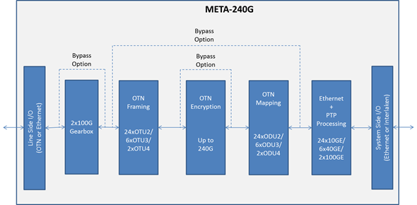 Source: PMC-Sierra
Adding OTN to a router delivers several benefits, says PMC. OTN helps identify networking faults more quickly and simplifies the monitoring and enforcement of service-level agreements. OTN also includes forward-error correction which benefits optical link performance.
Ethernet is the default router protocol interface while OTN is the dominant protocol in the transport network, says PMC. By moving OTN onto the router’s line port, the transport network extends its end-point reach to the router, says Stephen Docking, senior product line manager, communications unit at PMC. This leads to faster fault isolation and fault recovery.
“The transport network can now communicate with the router in a standard way, providing an extra level of protection that is faster than just IP layer protection,” says Docking.
OTN also supports the monitoring of error rates across the link.“By making the router part of the link, the service provider can not only monitor performance within the transport network but across the entire end-to-end link including the router,” says Docking. Such monitoring helps verify service-level agreements.
Meta-240G features
The Meta-240G is PMC’s third-generation framer for routers. The previous generation device, the 120 gigabit Meta-120G was PMC’s first to support OTU4 100 gigabit frames and was implemented in 40nm CMOS.
The Meta-240G doubles the total bandwidth: 240 gigabit facing the front panel optics and 240 gigabit interfacing to the network processor on the router’s line card. The device can thus support two 100 gigabit interfaces, six 40 gigabit interfaces and 24, 10 gigabit interfaces. “You can even have two 100 Gig and one 40 Gig, or two 100 Gig and four 10 Gig but most customers will just use 100 Gig [interfaces],” says Docking.
PMC has doubled the framer’s capacity while keeping overall power consumption fixed, in effect halving the power per port compared to its previous generation Meta-120G framer. Yet the chip also supports new features including a low-latency AES-256 encryption engine and an on-chip gearbox. The Meta-240G achieves the power savings by making the chip in 28nm CMOS and by improving the serdes design.
The gearbox function translates between 10 gigabit streams and 25 gigabit ones. Many devices use 10 gigabit serdes but to connect to a CFP2 or CFP4 100 gigabit optical modules, 25 gigabit electrical channels are required.
“Designers have had to use discrete gearbox devices [on the line card] which adds space, power and cost,” says Docking. “With the Meta-240G, the gearbox function is integrated into the device.”
Given IP traffic trends, will a 400 gigabit Meta device be needed in 2017? “It may be a bit longer - two to three years’ time - but we would need to [have such a device] to follow the existing trend,” says Docking.
Further information
PMC advances OTN with 400 Gigabit processor, click here
Mellanox Technologies to acquire EZchip for $811M
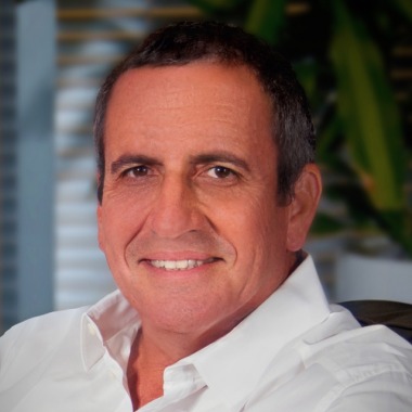 Eyal Waldman
Mellanox makes InfiniBand and Ethernet interconnection platforms and products for the data centre while EZchip sells network and multi-core processors that are used in carrier edge routers and enterprise platforms.
EZchip’s customers include Huawei, ZTE, Ericsson, Oracle, Avaya and Cisco Systems.
“Mellanox needs to diversify its business; it is still heavily dependent on the high-performance computing market and InfiniBand,” says Bob Wheeler, principal analyst, networking at market research firm The Linley Group. “EZchip helps move Mellanox into markets and customers that it would not have access to with its existing products.”
CEO Eyal Waldman says Mellanox will continue to focus on the data centre and not the WAN, and that it plans to use EZchip’s products to add intelligence to its designs. Mellanox's Ethernet expertise may also find its way into EZchip’s ICs.
But analysts do expect Mellanox to benefit from telecom. “The big change has to do with Network Function Virtualisation (NFV) and the fact that service provider’s data centres are starting to look more and more like cloud data centres,” says Wheeler. “There is an opportunity for Mellanox to start selling to the large carriers and that is a whole new market for the company.”
Acquiring EZchip
Both companies will ensure continuity and use the same product lines to grow into each other’s markets, said Waldman on a conference call to announce the deal: “Later on will come more combined solutions and products.” First product collaborations are expected in 2016 with more integrated products appearing from 2017.
“Mellanox sees a need to add intelligence to its core products and it does not really have the expertise or the intellectual property,” says Wheeler. One future product of interest is the smart or intelligence network interface controller (NIC). “By working together they could product quite a compelling product,” says Wheeler.
In 2014 EZchip acquired Tilera for $50 million. The value of the deal could have risen to $130 million but was dependent on targets that Tilera did not meet, says Wheeler. Tilera's products include multi-core processors, NICs and white box security appliances. EZchip has also announced the Tile-Mx product family using Tilera’s technology, the most powerful family device will feature 100, 64-bit ARM cores.
The primary application of Tilera’s products is security applications: deep-packet inspection and layer 7 processing. Instead of replacing the general-purpose processor in a security appliance, an alternative approach is to use an intelligent NIC card with a Tilera processor connected via the PCI Express bus to an Intel Xeon-based server. “The card can do a lot of the packet processing offloaded from the Xeon,” says Wheeler.
Another area where EZchip’s NPS processor can be used is in more dedicated appliances or in an intelligent top-of-rack switch. The NPS would perform security as well as terminating overlay protocols used for network virtualisation in the data centre. “You can terminate all those [overlay] protocols in a top-of-rack switch and offload that processing from the server,” says Wheeler.
The key benefit of InfiniBand is its very low latency but the flip side is that the protocol is limited with regard routing to larger fabrics. Adding intelligence could benefit Mellanox’s core Infiniband fabric products, notes Wheeler.
EZchip’s founder and CEO Eli Fruchter said he expects the merger to open doors for EZchip among more hyper-scale data centre players: “With the merger we believe we can be a lot more successful in data centres than by continuing by ourselves.”
Mellanox has made several acquisitions in recent years. It acquired data centre switch fabric player Voltaire in 2011, and in 2013 it added silicon photonics start-up Kotura and chip company IPTronics in quick succession. Now with EZchip's acquisition it will add packet processing and multi-core processor IP to its in-house technology portfolio.
The EZchip acquisition is expected to close in the first quarter of 2016.
Further information:
Mellanox’s Waldman: We've discussed merging for years, click here
Altera’s 30 billion transistor FPGA
- The Stratix 10 features a routing architecture that doubles overall clock speed and core performance
- The programmable family supports the co-packaging of transceiver chips to enable custom FPGAs
- The Stratix 10 family supports up to 5.5 million logic elements
- Enhanced security features stop designs from being copied or tampered with
Altera has detailed its most powerful FPGA family to date. Two variants of the Stratix 10 family have been announced: 10 FPGAs and 10 system-on-chip (SoC) devices that include a quad-core 64-bit architecture Cortex-A53 ARM processor alongside the programmable logic. The ARM processor can be clocked at up to 1.5 GHz.
The Stratix 10 family is implemented using Intel’s 14nm FinFET process and supports up to 5.5 million logic elements. The largest device in Altera’s 20nm Arria family of FPGAs has 1.15 million logic elements, equating to 6.4 billion transistors. “Extrapolating, this gives a figure of some 30 billion transistors for the Stratix 10,” says Craig Davis, senior product marketing manager at Altera.
 Altera's HyperFlex routing architecture. Shown (pointed to by the blue arrow) are the HyperFlex registers that sit at the junction of the interconnect traces. Also shown are the adaptive logic module blocks. Source: Altera.
The FPGA family uses a routing fabric, dubbed HyperFlex, to connect the logic blocks. HyperFlex is claimed to double the clock speed compared to designs implemented using Altera’s Stratix V devices, to achieve gigahertz rates. “Having that high level of performance allows us to get to 400 gigabit and one terabit OTN (Optical Transport Network) systems,” says Davies.
The FPGA company detailed the Stratix 10 a week after Intel announced its intention to acquire Altera for US $16.7 billion.
Altera is also introducing with the FPGA family what it refers to as heterogeneous 3D system packaging and integration. The technology enables a designer to customise the FPGA’s transceivers by co-packaging separate transceiver integrated circuits (ICs) alongside the FPGA.
Different line-rate transceivers can be supported to meet a design's requirements: 10, 28 or 56 gigabit-per-second (Gbps), for example. It also allows different protocols such as PCI Express (PCIe), and different modulation formats including optical interfaces. Altera has already demonstrated a prototype FPGA co-packaged with optical interfaces, while Intel is developing silicon photonics technology.
HyperFlex routing
The maximum speed an FPGA design can be clocked is determined by the speed of its logic and the time it takes to move data from one part of the chip to another. Increasingly, it is the routing fabric rather than the logic itself that dictates the total delay, says Davis.
This has led the designers of the Stratix 10 to develop the HyperFlex architecture that adds a register at each junction of the lines interconnecting the logic elements.
Altera first tackled routing delay a decade ago by redesigning the FPGA’s logic building block. Altera went from a 4-input look-up table logic building block to a more powerful 8-input one that includes output registers. Using the more complex logic element - the adaptive logic module (ALM) - simplifies the overall routing. “You are essentially removing one layer of routing from your system,” says Davies.
When an FPGA is programmed, the file is presented that dictates how the wires and hence the device’s logic are connected. The refinement with HyperFlex is that there are now registers at those locations where the switching between the traces occurs. A register can either be bypassed or used.
“It allows us to put the registers anywhere in the design, essentially placing them in an optimum place for a given route across the FPGA,” says Davies. The number of hyper-registers in the device's routing outnumber the standard registers in the ALM blocks by a factor of ten.
Using the registers, designers can introduce data pipelining to reduce overall delay and it is this pipelining, combined with the advanced 14nm CMOS process, that allows a design to run at gigahertz rates.
“We have made the registers small but they add one or two percent to the total die area, but in return it gives us the ability to go to twice the performance,” says Davies. “That is a good trade-off.
The biggest change getting HyperFlex to work has been with the software tools, says Davies. HyperFlex and the associated tools has taken over three years to develop.
“This is a fundamental change,” says Davies. “It [HyperFlex] is relatively simple but it is key; and it is this that allows customers to get to this doubling of core performance.”
The examples cited by Altera certainly suggest significant improvements in speed, density, power dissipation, but I want to see that in real-world designs
Loring Wirbel, The Linley Group
Applications
Altera says that over 100 customer designs have now been processed using the Stratix 10 development tools.
It cites as an example a current 400 gigabit design implemented using a Stratix V FPGA that requires a bus 1024-bits wide, clocked at 390MHz. The wide bus consumes considerable chip area and routing it to avoid congestion is non-trivial.
Porting the design to a Stratix 10 enables the bus to be clocked at 781MHz such that the bus width can be halved to 512 bits. “It reduces congestion, makes it easier to do timing closure and ship the design,” says Davies. “This is why we think Stratix 10 is so important for high-performance applications like OTN and data centres.” Timing closure refers to the tricky part of a design where the engineer may have to iterate to ensure that a design meets all the timing requirements.
For another, data centre design, a Stratix 10 device can replace five Stratix V ICs on one card. The five FPGAs are clocked at 250MHz, run PCIe Gen2 x8 interfaces and DDR3 x72 memory clocked at 800MHz. Overall the power consumed is 120W. Using one Stratix 10 chip clocked at 500MHz, faster PCIe Gen3 x8 can be supported as can a wider DDR3 x144 memory clocked at 1.2GHz, with only 44W consumed.
Loring Wirbel, senior analyst at The Linley Group, says that Altera’s insertion of pipelined registers to cut average trace lengths is unique.
“The more important question is, can the hyper-register topology regularly gain the type of advantages claimed?” says Wirbel. “The examples cited by Altera certainly suggest significant improvements in speed, density, power dissipation, but I want to see that in real-world designs.”
We are also looking at optical transceivers directly connected to the FPGA
Craig Davies, Altera
Connectivity tiles
Altera recognises that future FPGAs will support a variety of transceiver types. Not only are there different line speeds to be supported but also different modulation schemes. “You can’t build one transceiver that fits all of these requirements and even if you could, it would not be an optimised design,” says Davies.
Instead, Altera is exploiting Intel’s embedded multi-die interconnect bridge (EMIB) technology to interface the FPGA and transceivers, dubbed connectivity tiles. The bridge technology is embedded into the chip’s substrate and enables dense interconnect between the core FPGA and the transceiver IC.
Intel claims fewer wafer processing steps are required to make the EMIB compared to other 2.5D interposer processes. An interposer is an electrical design that provides connectivity. “This is a very simple ball-grid sort of interposer, nothing like the Xilinx interposer,” says Wirbel. “But it is lower cost and not intended for the wide range of applications that more advanced interposers use.”
Using this approach, a customer can add to their design the desired interface, including optical interfaces as well as electrical ones. “We are also looking at optical transceivers directly connected to the FPGA,” says Davies.
Wirbel says such links would simplify interfacing to OTN mappers, and data centre designs that use optical links between racks and for the top-of-rack switch.
“Intel wants to see a lot more use of optics directly on the server CPU board, something that the COBO Alliance agrees with in part, and they may steer the on-chip TOSA/ ROSA (transmitter and receiver optical sub-assembly) toward intra-board applications,” he says.
But this is more into the future. “It's fine if Intel wants to pursue those things, but it should not neglect common MSAs for OTN and Ethernet applications of a more traditional sort,” says Wirbel.
The benefit of the system-in-package integration is that different FPGAs can be built without having to create a new expensive mask set each time. “You can build a modular lego-block FPGA and all that it has different is the packaged substrate,” says Davies.
Security and software
Stratix 10 also features security features to protect companies’ intellectual property from being copied or manipulated.
The FPGA features security hardware that protects circuitry from being tampered with; the bitstream that is loaded to configure the FPGA must be decrypted first.
The FPGA is also split into sectors such that parts of the device can have different degrees of security. The sectoring is useful for cloud-computing applications where the FPGA is used as an accelerator to the server host processor. As a result, different customers’ applications can be run in separate sectors of the FPGA to ensure that they are protected from each other.
The security hardware also allows features to be included in a design that the customer can unlock and pay for once needed. For example, a telecom platform could be upgraded to 100 Gigabit while the existing 40 Gig live network traffic runs unaffected in a separate sector.
Altera has upgraded its FPGA software tools in anticipation of the Stratix 10. Features include a hierarchical design flow to simplify the partitioning of a design project across a team of engineers, and the ability to use cloud computing to speed up design compilation time.
What applications will require such advanced FPGAs, and which customers will be willing to pay a premium price for? Wirbel says the top applications will remain communications.
“The emergence of new 400 Gig OTN transport platforms, and the emergence of all kinds of new routers and switches with 400 Gig interfaces, will keep a 40 percent communication base for FPGAs overall solid at Altera,” he says.
Wirbel also expects server accelerator boards where FPGA-based accelerators are used for such applications as financial trading and physics simulation will also be an important market. “But Intel must consider the accelerator board market as an ideal place for Stratix 10 on its own, and not merely as a vehicle for promoting a future Xeon-plus-FPGA hybrid,” he says.
Altera will have engineering samples of the Stratix 10 towards the end of 2015, before being shipped to customers.
Moore's law and silicon photonics
Chip pioneer Gordon E. Moore’s article appeared in the magazine Electronics in 1965. Dr. Moore was the director of the R&D labs at Fairchild Semiconductor, an early maker of transistors. Moore went on to co-found Intel, then a memory company, becoming its second CEO after Robert Noyce.
Moore’s article was written in the early days of integrated circuits. At the time, silicon wafers were one inch in diameter and integrating 50 components on a chip was deemed a state-of-the-art design.
Moore observed that, at any given time, there was an ideal number of components that achieved a minimum cost. Add a few more components and the balance would be tipped: the design would become overly complex, wafer yields would go down and costs would rise.
His key insight, later to become known as Moore’s law, was that integrated circuit complexity at this minimum cost was growing over time. Moore expected the complexity to double each year for at least another decade.
In his article he predicted that, by 1970, the manufacturing cost per component would be a tenth of the cost in 1965. Extrapolating the trend further, Moore believed that “by 1975, the number of components per integrated circuit for minimum cost will be 65,000 components.” Moore was overly optimistic, but only just: in 1975, Intel was developing a chip with 32,000 transistors.
“Perhaps we can say that the future of silicon photonics is the future of electronics itself.”
One decade after his article, Moore amended his law to a doubling of complexity every 24 months. By then the industry had started talking about transistors rather than components - circuit elements such as transistors, resistors and capacitors - after alighting on complementary metal oxide semiconductor (CMOS) technology to make the bulk of its chips. And in the years that followed, the period of complexity-doubling settled at every 18 months.
Moore has received less credit for his article's remarkable foresight regarding the importance of integrated circuits, especially when, in 1965, their merits were far from obvious. Such devices would bring a proliferation of electronics, he said, “pushing this science into many new areas”.
He foresaw home computers “or at least terminals connected to a central computer’, automatic control for automobiles and even mobile phones - ‘personal portable communications equipment’ as he called them. The biggest potential of ICs, he said, would be in the making of systems, with Moore highlighting computing, and telephone communications and switches.
The shrinking transistor
The shrinking of the transistor has continued ever since. And the technological and economic consequences have been extraordinary.
As a recent 50th anniversary Moore’s law article in IEEE Spectrum explains (link above), the cost of making a transistor in 1965 was $30 at today’s costs, in 2015 it is one billionth of a dollar. And in 2014, the semiconductor industry made 250 billion billion transistors, more transistors than had been made in all the years of the semiconductor industry up to 2011.
But the shrinking of the transistor cannot continue indefinitely, especially as certain transistor dimensions approach the atomic scale. As a result, many of the benefits that resulted with each shift to a new, smaller feature-sized CMOS process no longer hold.
To understand why, some understanding of CMOS and in particular, the MOS field effect transistor (MOSFET), is required.
Current flow between a MOSFET’s two terminals - the source and the drain - is controlled by a voltage placed on a third, electrical contact known as a gate. The gate comprises a thin layer of metal oxide, an oxide insulator on which sits a metal contact.
Several key dimensions define the MOSFET including the thickness of the oxide, the width of the source and the drain, and the gate length - the distance between the source and the drain.
Dennard scaling, named after IBM engineer and inventor of the DRAM, Robert Dennard, explains how the key dimensions of the transistor can all shrunk by the same factor, generation after generation. It is the effect of this scaling that makes Moore’s law work.
From the 1970s to the early 2000s, shrinking the transistor’s key dimension by a fixed factor returned a guaranteed bounty. More transistors could be placed on a chip allowing more on-chip integration, while each transistor became cheaper.
In turn, for a given chip area, the chip’s power density - the power consumption over a given area - remained constant. There may be more transistors crammed into a fixed area but the power each one consumes is less.
The predictable era of scaling transistors, after 50 years, is coming to an end and the industry is set to change
The transistor gate length feature size is used to define the CMOS technology or process node. In 1980, the minimum feature size was around 3 microns, nowadays CMOS chips typically use a 28 nanometer feature size - a 100 fold reduction. The metal oxide thickness has also been reduced one hundred times over the years.
But in the last decade Dennard scaling has come to an end.
The gate’s oxide thickness can no longer be trimmed as its dimensions are only a few atoms thick. The voltage threshold, the voltage applied to the gate to turn the transistor on, has also stopped shrinking, which in turn has stopped the scaling of the transistor’s upper voltage.
Why is this important? Because no longer being able to scale all these key parameters has meant that while smaller transistors can still be made, their switching speed is no longer increasing, nor is the power density constant.
Moreover, the very success of the relentless scaling means that the transistors are so tiny that new effects have come into play.
Transistors now leak current even when they are in the ‘off’ state. This means they consume power not only when they are being switched at high speed - the active power - but also they consume leakage power when they are off due to this current.
Process engineers now must work harder, to develop novel transistor designs and new materials to limit the leakage current. A second issue associated with the prolonged success of Dennard scaling is variability. Transistors are now less reliable and their performance less predictable.
The end of Dennard scaling means that the chip companies’ motivation to keep shrinking transistors is more to do with device cost rather than performance.
If, before, the power density stayed fixed with each new generation of CMOS process, more recently it has been the cost of manufacturing of a given area of silicon that has stayed fixed.
As the IEEE Spectrum Moore’s law article explains, this has been achieved by a lot of engineering ingenuity and investment. Device yield has gone up from 20 percent in the 1970s to between 80 and 90 percent today. The size of the silicon wafers on which the chips are made has also increased, from 8 inches to 12 inches. And while the lithography tools now cost one hundred-fold more than 35 years ago, they also pattern the large wafers one hundred times faster.
But now even the cost of making a transistor has stopped declining, according to The Linley Group, with the transition point being around the 28nm and 20nm CMOS.
Silicon manufacturing innovation will continue, and transistors will continue to shrink. Leading chip companies have 14nm CMOS while research work is now at a 7nm CMOS process. But not everyone will make use of the very latest processes, given how these transistors will be more costly.
Beyond Moore’s law
The industry continues to debate how many years Moore’s law still has. But whether Moore’s law has another 10 years or not, it largely does not matter.
Moore’s law has done its job and has brought the industry to a point where it can use billions of transistors for its chip designs.
But to keep expanding computing performance, new thinking will be required at many levels, spanning materials, components, circuit design, architectures and systems design.
The predictable era of scaling transistors, after 50 years, is coming to an end and the industry is set to change.
IBM announced last year its plan to invest US $3 billion over five years to extend chip development. Areas it is exploring include quantum computing, neurosynaptic computing, III-V technologies, carbon nanotubes, graphene, next-generation low-power transistors, and silicon photonics.
Silicon photonics
The mention of silicon photonics returns us to Gordon Moore’s 1965 article. The article starts with a bang: “The future of integrated electronics is the future of electronics itself".
Can the same be said of photonics?
Is the future of integrated photonics the future of photonics itself?
Daryl Inniss, vice president of Ovum’s components practice, argues this is certainly true. Photonics may not have one optical building block like electronics has the transistor, nor is there any equivalent of Dennard scaling whereby shrinking photonic functions delivers continual performance benefits.
But photonic integration does bring cost benefits, and developments in optical interconnect and long-haul transmission are requiring increasing degrees of integration, the sort of level of component integration associated with the chip industry at the time of Moore’s article.
And does the following statement hold true? “The future of silicon photonics is the future of photonics itself.”
“I think silicon photonics is bigger than photonics itself,” says Inniss. “Where do you draw the line between photonics and electronics? IBM, Intel and STMicroelectronics are all suppliers of electronics.”
Inniss argues that silicon photonics is an electronics technology. “Perhaps we can say that the future of silicon photonics is the future of electronics itself.”
PMC advances OTN with 400 Gigabit processor
Optical modules for the line-side are moving beyond 100 Gigabits to 200 Gigabit and now 400 Gigabit transmission rates. Such designs are possible thanks to compact photonics designs and coherent DSP-ASICs implemented using advanced CMOS processes.
 An example switching application showing different configurations of the DIGi-G4 OTN processor on the line cards. Source: PMC
For engineers, the advent of higher-speed line-side interfaces sets new challenges when designing the line cards for optical networking equipment. In particular, the framer silicon that interfaces to the coherent DSP-ASIC, on the far side of the optics, must cope with a doubling and quadrupling of traffic.
Such line cards for metro network platforms is where PMC-Sierra is targeting its latest 400 Gigabit DIGI-G4 Optical Transport Network (OTN) processor.
The OTN standard, defined by the telecom standards body of the International Telecommunication Union (ITU-T), performs several roles in the network. It is a layer-one technology that packages packet and circuit-switched traffic. OTN wraps traffic in a variety of container sizes for transport, from 1 Gigabit (OTU1) to 100 Gigabit (OTU4). And now 100 Gigabit can be viewed as a sub-frame, multiples of which can be combined to create even larger frames, dubbed OTUCn, where n is a multiple of 100 Gig.
Using OTN, container traffic can be broken up, switched and recombined within new containers before being transmitted optically. OTN also provides forward error correction and network management features.
PMC’s DIGI-G4 OTN processor is aimed at next-generation packet-optical transport systems (P-OTS) adopting 400 Gig line cards, and for platforms for the burgeoning data centre interconnect market.
“The amounts of traffic internet content providers need between their data centres is astonishing; they are talking hundreds of terabits of traffic,” says Hamish Dobson, director of strategic marketing at PMC. Hyper-scale data centre operators, unlike telcos, do not require OTN switching but they are keen on OTN as the DWDM management layer, he says: “I’m not aware of any of the hyper-scale players who are deploying their own networks who are not using OTN as the un-channelised digital wrapper on their systems.”
The DIGI-G4 does more than simply quadruple OTN traffic throughput compared to PMC’s existing DIGI 120G OTN processor. The chip also adds encryption hardware to secure links while supporting the emerging Transport Software-Defined Networking (Transport SDN).
DIGI-G4
The DIGI-G4 increases by fourfold the traffic throughput while halving the power-per-port compared to PMC's DIGI 120G. System designers must control the total power consumption of the line card, given the greater interface density, and when metro equipment platforms’ power profile is already at 500W-per-slot, says Dobson. PMC has halved the power consumption-per-port by implementing the latest OTN processor in a 28 nm CMOS process and by using more power-efficient serialisers/ deserialisers (serdes).
Internet content providers with their use of distributed data centres is one reason for the device’s introduction of the Advanced Encryption Standard (AES-256). Another is the emergence of cloud services and the need to secure individual customer’s traffic.
“We have added a channelised hardware [encryption] engine,” says Dobson. “The encryption engine is capable of being applied to any OTN channel in the device.”
Other features of the Digi-G4 include input/ output (I/O) capable of 28 Gigabit-per-second (Gbps). This enables the DIGI-G4 to connect directly to CFP2 and CFP4 pluggable optics without the need for gearbox devices on the line card, reducing power and overall cost.
The OTN chip is a hybrid design capable of processing 400 Gigabit of packet traffic or 400 Gig of circuit (time-division multiplexed) traffic, or any combination of the two, with a granularity of one gigabit channels. “It can switch a full 400 Gig's worth of one Gigabit ODU0 channels,” says Dobson.
The Digi-G4 also support a pre-standard implementation of the OTUC2 and OTUC4 transport units that are two and four multiples of 100 Gigabit, respectively. The OTUCn standard is not expected to be ratified before 2017.
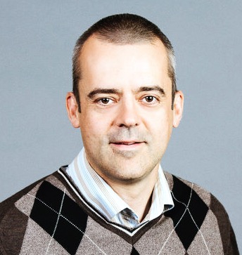
We will see the capabilities of these new packet-optical systems coming together with SDN to enable interesting things to be done in the metro
Hamish Dobson
Transport SDN
SDN will have a significant effect on the transport network, says Dobson. In particular Transport SDN where SDN is applied to the transport layers of the wide area network (WAN). As such, OTN plays an important role in multi-layer optimisation. Packet-optical transport systems, which support packet and optical within the same platform, are ideal for getting much more efficiency out of the optical spectrum, he says.
Using Transport SDN to co-ordinate packet, OTN and the optical layer, routing decisions can be made aware of available capacity in the optical domain. In turn, network protection decisions can also be based on optical capacity availability. “The DIGI-G4, being a hybrid processor to enable these multi-layer platforms, is an important element to bring this all together,” says Dobson.
OTN also aids the virtualisation of optical resources whereby individual enterprises can be given a simpler, subset view of the network. “We need more than just wavelength granularity in the network,” says Dobson. Since 100 Gigabit and, in future, 200 and 400 Gig lightwaves, are such large pipes, these are inevitably filled with multiple traffic flows. “Channelised OTN and OTN switching are how carriers are going to break down these massive amounts of optical capacity and partition them for various uses,” says Dobson.
A third element whereby OTN aids Transport SDN is the move to on-demand provisioning by adapting capacity at the OTN layer. Dobson cites the ITU-T G.7044/Y.1347 (G.HAO) standard, which the DIGI-G4 supports, whereby frame size can be adjusted using ODUflex without impacting existing network traffic.
“We will see the capabilities of these new packet-optical systems coming together with SDN to enable interesting things to be done in the metro,” says Dobson.
Samples of the DIGI-G4 are already with customers.
Further reading
White Paper: Benefits of OTN in Transport SDN, click here and then 'documentation'