
OFC 2024 industry reflections: Final part
Chris Cole, Consultant
OFC and optics were back with a vengeance. The high level of excitement and participation in the technical and exhibit programmes was fueled by artifical intelligence/ machine learning (AI/ML). To moderate this exuberance, a few reality checks are offered.
During the Optica Executive Forum, held on the Monday, one of the panels was with optics industry CEOs. They were asked if AI/ML is a bubble. All five said no. They are right that there is a real, dramatic increase in optics demand driven by AI/ML, with solid projections showing exponential growth.
At the same time, it is a bubble because of the outrageous valuations for anything with an AI/ML label, even on the most mundane products. Many booths in the Exhibit Hall had AI/ML on their panels, for the same product types companies have been showing for years. Some of the start-ups and public companies presenting and exhibiting at OFC have frothy valuations by claiming to solve compute bottlenecks. An example is optically interconnecting memory, which sends investors into a frenzy, as if this has not been considered for decades.
The problem with a bubble is that it misallocates resources to promises of near-term pay off, at the expense of investment into long-term fundamental technology which is the only way to enable a paradigm shift to optical AI/ML interconnect.
I presented a version of the below table at the OFC Executive Forum, pointing out that there have only been two paradigm shifts in optical datacom, and these were enabled by fundamentally new optical components and devices which took decades to develop.
My advice to investors was to be skeptical of any optically-enabled breakthrough claims which simply rearrange or integrate existing components and devices. As with previous bubbles, this one will self-correct, and many of the stratospheric valuations will collapse.
Source: Chris Cole
A second dose of reality was provided by Ashkan Seyedi of Nvidia, in several OFC forums, illustrated by the Today’s Interconnect Details table below (shared with permission).
Source: Ashkan Seyedi, Nvidia
He pointed out that the dominant AI/ML interconnect continues to be copper because it beats optics by integer or decade better metrics of bandwidth density, power, and cost. Existing data centre optical networking technology cannot simply be repackaged as optical compute input-output (I/O), including optical memory interconnect, because that does not beat copper.
A third dose of reality came from Xiang Zhou of Google and Qing Wang of Meta in separate detailed analysis presented at the Future of LPO (Linear Pluggable Optics) Workshop. They showed that not only does linear pluggable optics have no future beyond 112 gigabits per lane, but even at that rate it is highly constrained, making it unsuitable for general data centre deployment.
Yet linear pluggable optics was one of the big stories at OFC 2024, with many highly favourable presentations and more than two dozen booths exhibiting it in some form. This was the culmination of a view that has been advanced for years that optics development is too slow, especially if it involves standards. LPO was moved blazingly fast into prototype hardware without being preceded by extensive analysis. The result was predictable as testing in typical large deployment scenarios found significant problems.
At OFC 2025, there will be few if any linear pluggable optics demos. And it will not be generally deployed in large data centres.
Coincidently, the OIF announced that it started a project to standardise optics with one digital signal processor (DSP) in the link, located in the transmitter. This was preceded by analysis, including by Google and Meta, showing good margin against the types of impairments found in large data centres. The expectation is that many IC vendors will have DSP on transmit-only chips soon, including likely at OFC 2025.
A saving grace of linear pluggable optics may be the leveraging of related OIF work on linear receiver specification methodology. Another benefit may be the reaffirmation that real progress in optics is hard and requires fundamental understanding. Shortcutting of well-established engineering practices leads to wasted effort.
Real advances require large investment and take many years, which is what is necessary for optical AI/ML compute interconnect. Let’s hope investors realise this.
Hojjat Salemi, Chief Business Development Officer, Ranovus
Hyperscalers are increasingly recognising that scaling AI/ML compute demands extensive optical connectivity, and the conventional approach of using pluggable optical modules is proving inadequate.
The network infrastructure plays a pivotal role in the compute architecture, with various optimisation strategies depending on the workload. Both compute scale-up and scale-out scenarios necessitate substantial connectivity, high-density beach-front, cost-effectiveness, and energy efficiency. These requirements underscore the advantages of co-packaged optics (CPO) in meeting the evolving demands of AI/ML compute scaling.
It is great to see prominent tier-1 vendors like Nvidia, AMD, Broadcom, Marvell, GlobalFoundries, and TSMC embracing co-packaged optics. Their endorsement shows a significant step forward, indicating that the supply chain is gearing up for high-volume manufacturing by 2026. The substantial investments being poured into this technology underscore the collective effort to address the pressing challenge of scaling compute efficiently. This momentum bodes well for the future of AI/ML compute infrastructure and its ability to meet the escalating demands of various applications.
What surprise me was how fast low-power pluggable optics fizzled. While initially shown as a great technology, linear pluggable optics ultimately fell short in meeting some critical requirements crucial to Hyperscalers. Although retimed pluggable optical modules have been effective in certain applications and are likely to continue serving those needs for the foreseeable future, the evolving demands of new applications such as scaling compute necessitate innovative solutions like co-packaged optics.
The shift towards co-packaged optics highlights the importance of adapting to emerging technologies that can better address the unique challenges and requirements of rapidly evolving industries like hyperscale computing.
Harald Bock, Vice President Network Architecture, Infinera
I am impressed by the range of topics, excellent scientific work and product innovation each time I attend OFC.
Normally, the show's takeaways differ among the participants that I talk to. This year, most of the attendees I chatted agreed on the main topics. The memorable items this year ranged from artificial intelligence (AI) data centres, 800 gigabit-per-second (Gbps) pluggables, to the Full Spectrum Concert at Infinera’s OFC party that was held on the USS Midway.
AI is becoming the key driver for network capacity. While we are a very technology-driven industry, the interest in different technologies is driven by the business opportunities we expect. This puts AI at the top of the list. It is not the AI use cases in network operations, planning, and analytics, which are all progressing, but rather the impact that deploying AI data centres will have on network capacity and particularly on optical interfaces within and between data centres.
The interest was clearly amplified by the fact that recovery of the telecom networks business is only expected in the year’s second half.
Short term, AI infrastructure creates massive demand for short-reach interconnect within data centres, with longer-reach inter-data centre connectivity also being driven by new buildouts. So, we can expect AI to be the key driver of network bandwidth in the coming years.
It is in this context that linear pluggable optics has become an important candidate technology to provide efficient, low-energy interconnect, and as a result, it generated a huge amount of interest this year, stealing some of the attention that co-packaged optics or similar approaches have received in the past. Overall, AI use cases drove huge interest in 800Gbps pluggable optics products and demonstrations at the show.
Reducing interface and network power consumption have become key industry objectives. In all of these use cases and products, power consumption is now the main optimisation goal in order to drive down overall data centre power or to fit all pluggable optics into the same existing form factors (QSFP-DD and OSFP), even at higher rates such as 1.6Tbps.
I do believe that reducing power consumption, be it per capacity, or per reach x capacity depending on use case, has become our industry’s main objective. Looking at projected capacity growth that will continue at 35 to 40 per cent per year across much of cloud networks, that is what we all should be working on.
Another observation is that power consumption and capacity per duct have replaced spectral efficiency as the figure of merit. You could say that this is starting to replace the objective of increasing fibre capacity that our industry has been working under for many years.
We have all discussed the fact that we are no longer going to be able to easily increase spectral efficiency as we are approaching Shannon’s limit. In order to further increase fibre capacity, we have been talking about additional wavelength bands, with products now achieving beyond 10-terabit transmission bandwidth with Super C- and Super L-band and the option to add the S-, O-, and U- bands, as well as about spatial division multiplexing, which today refers to the use of multiple fibre cores to transmit data.
Before OFC, I was puzzled about the steps we, as an industry, would take since all of these require more than a single product from one company. Indeed it is an ecosystem of related components, amplifiers, wavelength handling, even splicing procedures. After OFC, I am now confident that uncoupled multi-core fibre is a good candidate for a next step, with progress on additional wavelength bands not at all out of the picture.
There is one additional point I learned from looking at this topic. In real-world deployments today, multi-core fibre will accelerate a massive increase in parallel fibres that are being deployed in fibre ducts across the world. To me, that means that while we are going to all focus on power consumption as a key measure for innovation, we should really use capacity per duct as an additional figure of merit.
In terms of technological progress, I would like to call out the area of quantum photonics.
We all saw the results from an impressive research push in this area, with complex photonic integration and interesting use cases being explored. The amount of work done in this area makes it difficult for me to keep up to speed. I continue to be fascinated and excited about the work done.
An entirely different category of innovation was shown in the post-deadline session where Microsoft and University of Southampton presented hollow-core fiber with a record 0.11 dB/km fiber loss. While we have been talking about the great promise of anti-resonant hollow-core fiber for a while as it offers significantly reduced latency, it reduces signal distortion by removing nonlinearity and offering low dispersion. All that has been shown before, but achieving a fibre loss that is considerably lower than that of all other fibre types is excellent news.
It confirms that hollow-core fiber could change the systems and the networks we build, and I will continue to keep close tabs on the progress in this area.
Overall, OFC 2024 was a great show, with my company launching new products and having a packed booth full of visitors, a large number of customer engagements, and meetings with most of our suppliers.
I left San Diego already looking forward to next year's OFC.

OFC 2024 industry reflections: Part 4
Gazettabyte is asking industry figures for their thoughts after attending the recent OFC show in San Diego. This penultimate part includes the thoughts of Cisco’s Ron Horan, Coherent’s Dr. Sanjai Parthasarathi, and Adtran’s Jörg-Peter Elbers.

Ron Horan, Vice President Product Management, Client Optics Group, Cisco
Several years ago, no one could have predicted how extensive the network infrastructure required to support artificial intelligence (AI) and machine learning (ML) back-end networks in data centres would be. This year’s OFC answered that question. In a word, immense.
By 2025, the optics total addressable market for AI/ML back-end networks is expected to equal the already substantial front-end network optics market. By 2027, the back-end network optics total addressable market is projected to significantly exceed that of the front-end network. Additionally, the adoption of higher speeds and interface densities in the AI/ML back-end network will likely surpass that of the front-end.
Last year, linear pluggable optics (LPO) advocates heralded the power and cost savings associated with removing the digital signal processor (DSP) from an optics module and driving it directly from the host ASIC. Cisco and others have shown, using data and demos, that the overall power and cost savings are significant. However, in the last year, enthusiasm for this disruptive technology has been checked as concerns about link robustness and accountability have surfaced.
Enter linear receive optics (LRO), where the transmit path gets retimed while the high-power module receiver path moves to a linear receiver, which drives directly to the host ASIC. While not as power or cost friendly as linear pluggable optics, it does reduce power and some cost from the module compared to a fully retimed module while providing some diagnostic support for the link.
Only time and significant interoperability testing will determine whether linear pluggable optics or linear receive links will be robust enough to make them deployable at scale. Additionally, today’s linear pluggable and linear receive solutions have only been shown at 100 gigabits per lane. It is unclear whether 200 gigabits per lane for both approaches can work. Many think not. If not, then 100 gigabit per lane linear pluggable and linear receive optics may be a one-generation technology that is never optimal. The LPO-MSA, an industry effort that included many of the industry’s key companies, was announced before OFC to specify and resolve interoperability and link accountability concerns.
The overall concern about reducing power in the data centre was a strong theme at the show. The linear pluggable optics/ linear receive optics theme was born from this concern. As optics, switches, routers, and GPU servers become faster and denser, data centres cannot support the insatiable need for more power.
However, end users and equipment manufacturers seek alternative ways to lower power, such as liquid cooling and immersion. Liquid cooling uses liquid-filled pipes to remove the heat, which can help cool the optics. Liquid immersion further amplifies the cooling approach by immersing the optics, along with the host switch or GPU server, directly into an inert cooling fluid or placing them just above the fluid in the vapour layer. The ultimate result is to operate the optics at a lower case temperature and save power. It seems each customer is approaching this problem differently.
Last year’s OFC produced the first optics with 200 gigabit per optical lane technology. These solutions assumed a gearbox to a host interface that used 100-gigabit electrical channels. While some early adopters will use systems and optics with this configuration, a more optimal solution using 200 gigabits per lane electrical channels between the host and optics will likely be where we see 200 gigabits per lane optics hit their stride. This year’s show revealed a broader set of optics at 200 gigabit per lane rates. The technology maturity was markedly improved from last year’s early feasibility demos.
This is an exciting time in the optics industry. I look forward to learning what technologies will be introduced at OFC 2025.
Dr. Sanjai Parthasarathi, Chief Marketing Officer, Coherent
The progress in making 200-gigabit VCSELs ready for 200-gigabit PAM-4 optical transmission was a pleasant surprise of the event.
We at Coherent presented a paper on our lithographic aperture VCSEL, while Broadcom’s presentation outlined the technical feasibility of 200-gigabit PAM4 links. While both mentioned that more work is needed, the historic success of VCSEL-based links in short-reach interconnects suggests that the arrival of 200G-capable VCSELs will significantly impact the datacom market.
The feasibility of linear pluggable optics has likely delayed the market acceptance of co-packaged optics. There seems to be widespread consensus that LPO can reduce cost and power while retaining all the advantages of pluggable transceivers – a vibrant ecosystem, deployment flexibility, and a clear distinction of link accountability.
Jörg-Peter Elbers, senior vice president, advanced technology, standards and IPR, Adtran.
At this year’s OFC, discussions were much hotter than the weather. Who would have anticipated rain, winds and chilly temperatures in an always-sunny San Diego?
AI infrastructure created the most buzz at OFC. Accelerated compute clusters for generative AI are expected to drive massive demands for high-speed interconnects inside cloud-scale data centres. Consequently, 800-gigabit, 1.6-terabit, and future 3.2-terabit pluggable optical transceivers for front-end and back-end data centre fabrics stirred a lot of interest. Progress on co-packaged optics was also exciting, yet the technology will only go into deployments where and when pluggable transceivers hit unsurmountable challenges.
Silicon Photonics, indium phosphide, thin-film lithium niobate and VCSEL-based optics compete for design slots in a very competitive intra-data centre market, leading to new partnerships across the pluggable transceiver value chain. Linear receive optics and linear transmit & receive pluggable optics offer opportunities to reduce or eliminate DSP functions where electrical signal integrity permits.
While green ICT (information and communications technology) received a lot of attention at the conference, comments at the OFC Rump Session on this topic were somewhat disenchanting: time-to-market and total-cost-of-ownership drive deployment decisions at hyperscale data centres; lower energy consumption of optics is welcome but not a sufficient driver for architectural change.
On the inter-data centre side, a range of companies announced or demonstrated 800G-ZR/ZR+ transceivers at the show. More surprising was the number of transceiver vendors – including those not traditionally active in this market domain – who have added 400G-ZR QSFP-DD transceivers to their product portfolio. This indicates that the prices of these transceivers may decline faster than anticipated.
As for the next generation, industry consensus is building up behind a single-wavelength 1.6T ZR/ZR+ ecosystem using a symbol rate of some 240 gigabaud. There was a period in which indium phosphide and silicon photonics seemed to have taken over, and LiNbO3 appeared old-fashioned. With the move to higher symbol rates, LiNbO3 – in the form of thin-film Lithium Niobate – is celebrating a comeback: “Lithium Niobate is dead – long live Lithium Niobate!”
The OIF’s largest ever interop demo impressively showed how 400G-ZR+ modules can seamlessly interoperate over long-haul distances using an open-line system optimized for best performance and user-friendly operation. Monitoring and controlling such pluggable modules in IPoWDM scenarios can create operational and organizational challenges and is the subject of ongoing debates in IETF, TIP and OIF. A lean demarcation unit device can be a pragmatic solution to overcome these challenges in the near term. In the access/aggregation domain, the interest in energy-efficient 100G-ZR solutions keeps growing.
As the related OFC workshop showed, growing is also the support for a coherent single-carrier PON solution as the next step in the PON roadmap after 50Gbps very high-speed PON (VHSP).
Overall, there was excitement and momentum at OFC, with the conference and show floor returning to pre-Covid levels.
This is a good basis for the 50th anniversary edition of ECOC, taking place in Frankfurt, Germany, on September 22-26, 2024.
AI and optics: An OFC conversation

An OFC conversation with Adtran's Gareth Spence and consultant Daryl Inniss about the AI opportunity for photonics, click here.

OFC 2024 industry reflections: Part 2
Gazettabyte is asking industry figures for their thoughts after attending the recent OFC show in San Diego. Here are the thoughts from Ciena, Celestial AI and Heavy Reading.
Dino DiPerna, Senior Vice President, Global Research and Development at Ciena.
Power efficiency was a key theme at OFC this year. Although it has been a prevalent topic for some time, it stood out more than usual at OFC 2024 as the industry strives to make further improvements.
There was a vast array of presentations focused on power efficiency gains and technological advancements, with sessions highlighting picojoule-per-bit (pJ/b) requirements, high-speed interconnect evolution including co-packaged optics (CPO), linear pluggable optics (LPO), and linear retimer optics (LRO), as well as new materials like thin-film lithium niobate, coherent transceiver evolution, and liquid cooling.
And the list of technologies goes on. The industry is innovating across multiple fronts to support data centre architecture requirements and carbon footprint reduction goals as energy efficiency tops the list of network provider needs.
Another hot topic at OFC was overcoming network scale challenges with various explorations in new frequency bands or fibre types.
One surprise from the show was learning of the achievement of less than 0.11dB/km loss for hollow-core optical fibre, which was presented in the post-deadline session. This achievement offers a new avenue to address the challenge of delivering the higher capacities required in future networks. So, it is one to keep an eye on for sure.
Preet Virk, Co-founder and Chief Operating Officer at Celestial AI.
This year’s OFC was all about AI infrastructure. Since it is an optical conference, the focus is on optical connectivity. A common theme was how interconnect bandwidth is the oxygen for AI infrastructure. Celestial AI agrees fully with this and adds the memory capacity issue to deal with the Memory Wall problem.
Traditionally, OFC has focused on inter- and intra-data centre connectivity. This year’s OFC clarified that chip-to-chip connectivity is also a critical bottleneck. We discussed our high-bandwidth, low-latency, and low-power photonic fabric solutions for compute-to-memory and compute-to-compute connectivity, which were well received at the show.
It seemed that we were the only company with optical connectivity that satisfies bandwidths for high-bandwidth memory—HBM3 and the coming HBM4—with our optical chiplet.
Sterling Perrin, Senior Principal Analyst, Heavy Reading.
OFC is the premier global event for the optics industry and the place to go to get up to speed quickly on trends that will drive the optics industry through the year and beyond. There’s always a theme that ties optics into the overall communications industry zeitgeist. This year’s theme, of course, is AI. OFC themes are sometimes a stretch – think connected cars – but this is not the case for the role of optics in AI where the need is immediate. And the role is clear: higher capacities and lower power consumption.
The fact that OFC took place one week after Nvidia’s GTC event during which President and CEO Jensen Huang unveiled the Grace-Blackwell Superchip was a perfect catalyst for discussions about the urgency for 800 gigabit and 1.6 terabit connectivity within the data centre.
At a Sunday workshop on linear pluggable optics (LPO), Alibaba’s Chongjin Xie presented a slide comparing LPO and 400 gigabit DR4 that showed 50 per cent reduction in power consumption, a 100 per cent reduction in latency, and a 30 per cent reduction in production cost. But, as Xie and many others noted throughout the conference, LPO feasibility at 200 gigabit per lane remains a major industry challenge that has yet to be solved.
Another topic of intense debate within the data centre is Infiniband versus Ethernet. Infiniband delivers high capacity and extremely low latency required for AI training, but it’s expensive, highly complex, and closed. The Ultra Ethernet Consortium aims to build an open, Ethernet-based alternative for AI and high-performance computing. But Nvidia product architect, Ashkan Seyedi, was skeptical about the need for high-performance Ethernet. During a media luncheon, he noted that InfiniBand was developed as a high-performance, low-latency alternative to Ethernet for high-performance computing. Current Ethernet efforts, therefore, are largely trying to re-create InfiniBand, in his view.
The comments above are all about connectivity within the data centre. Outside the data centre, OFC buzz was harder to find. What about AI and data centre interconnect? It’s not here yet. Connectivity between racks and AI clusters is measured in meters for many reasons. There was much talk about building distributed data centres in the future as a means of reducing the demands on individual power grids, but it’s preliminary at this point.
While data centres strive toward 1.6 terabit, 400 gigabit seems to be the data rate of highest interest for most telecom operators (i.e., non-hyperscalers), with pluggable optics as the preferred form factor. I interviewed the OIF’s inimitable Karl Gass, who was dressed in a shiny golden suit, about their impressive coherent demo that included 23 suppliers and demonstrated 400ZR, 400G ZR+, 800ZR, and OpenROADM.
Lastly, quantum safe networking popped up several times at Mobile World Congress this year and the theme continued at OFC. The topic looks poised to move out of academia and into networks, and optical networking has a central role to play. I learned two things.
First, “Q-Day”, when quantum computers can break public encryption keys, may be many years away, but certain entities such as governments and financial institutions want their traffic to be quantum safe well in advance of the elusive Q-Day.
Second, “quantum safe” may not require quantum technology though, like most new areas, there is debate here. In the fighting-quantum-without-quantum camp, Israel-based start-up CyberRidge has developed an approach to transmitting keys and data, safe from quantum computers, that it calls photonic level security.

How scaling optical networks is soon to change
Carrier division multiplexing and spatial division multiplexing (CSDM) are both needed, argues Lumentum’s Brian Smith.
The era of coherent-based optical transmission as is implemented today is coming to an end, argues Lumentum in a White Paper.

Brian Smith
The author of the paper, Brian Smith, product and technology strategy, CTO Office at Lumentum, says two factors account for the looming change.
One is Shannon’s limit that defines how much information can be sent across a communications channel, in this case an optical fibre.
The second, less discussed regarding coherent-based optical transport, is how Moore’s law is slowing down.
”Both are happening coincidentally,” says Smith. “We believe what that means is that we, as an industry, are going to have to change how we scale capacity.”
Accommodating traffic growth
A common view in telecoms, based on years of reporting, is that internet traffic is growing 30 per cent annually. The CEO of AT&T mentioned over 30 per cent traffic growth in its network for the last three years during the company’s last quarterly report of 2023.
Smith says that data on the rate of traffic growth is limited. He points to a 2023 study by market research firm TeleGeography that shows traffic growth is dependent on region, ranging from 25 to 45 per cent CAGR.
Since the deployment of the first optical networking systems using coherent transmission in 2010, almost all networking capacity growth has been achieved in the C-band of a fibre, which comprises approximately 5 terahertz (THz) of spectrum.
Cramming more data into the C-band has come about by increasing the symbol rate used to transmit data and the modulation scheme used by the coherent transceivers, says Smith.
 The current coherent era – labelled the 5th on the chart – is coming to an end. Source: Lumentum.
Pushing up baud rate
Because of the Shannon limit being approached, marginal gains exist to squeeze more data within the C-band. It means that more spectrum is required. In turn, the channel bandwidth occupied by an optical wavelength now goes up with baud rate such that while each wavelength carries more data, the capacity limit within the C-band has largely been reached.
Current systems use a symbol rate of 130-150 gigabaud (GBd). Later this year Ciena will introduce its 200GBd WaveLogic 6e coherent modem, while the industry has started work on developing the next generation 240-280GBd systems.
Reconfigurable optical add-drop multiplexers (ROADMs) have had to become ‘flexible’ in the last decade to accommodate changing channel widths. For example, a 400-gigabit wavelength fits in a 75GHz channel while an 800-gigabit wavelength fits within a 150GHz channel.
Another consequence of Shannon’s limit is that the transmission distance limit for a certain modulation scheme has been reached. Using 16-ary quadrature amplitude modulation (16-QAM), the distance ranges from 800-1200km. Doubling the baud rate doubles the data rate per wavelength but the link span remains fixed.
“There is a fundamentally limit to the maximum reach that you can achieve with that modulation scheme because of the Shannon limit,” says Smith.
At the recent OFC show held in March in San Diego, a workshop discussed whether a capacity crunch was looming.
The session’s consensus was that, despite the challenges associated with the latest OIF 1600ZR and ZR+ standards, which promise to send 1.6 terabits of data on a single wavelength, the industry is confident that it will meet the OIF’s 240-280+ GBd symbol rates.
However, in the discussion about the next generation of baud rate—400-500GBd—the view is that while such rates look feasible, it is unclear how they will be achieved. The aim is always to double baud rate because the increase must be meaningful.
“If the industry can continue to push the baud rate, and get the cost-per-bit, power-per-bit, and performance required, that would be ideal,” says Smith.
But this is where the challenges of Moore’s law slowing down comes in. Achieving 240GBd and more will require a coherent digital signal processor (DSP) made using a 3nm CMOS process at least. Beyond this, transistors start to approach atomic scale and the performance becomes less deterministic. Moreover, the development costs of advanced CMOS processes – 3nm, 2nm and beyond – are growing exponentially.
Beyond 240GBd, it’s also going to become more challenging to achieve the higher analogue bandwidths for the electronics and optics components needed in a coherent modem, says Smith. How the components will be packaged is key. There is no point in optimising the analogue bandwidth of each component only for the modem performance to degrade due to packaging. “These are massive challenges,” says Smith.
This explains why the industry is starting to think about alternatives to increasing baud rate, such as moving to parallel carriers. Here a coherent modem would achieve a higher data rate by implementing multiple wavelengths per channel.
Lumentum refers to this approach as carrier division multiplexing.
Capacity scaling
The coherent modem, while key to optical transport systems, is only part of the scaling capacity story.
Prior to coherent optics, capacity growth was achieved by adding more and more wavelengths in the C-band. But with the advent of coherent DSPs compensating for chromatic and polarisation mode dispersion, suddenly baud rate could be increased.
“We’re starting to see the need, again, for growing spectrum,” says Smith. “But now, we’re growing spectrum outside the C-band.”
First signs of this are how optical transport systems are adding the L-band alongside the C-band, doubling a fibre’s spectrum from five to 10THz.
“The question we ask ourselves is: what happens once the C and L bands are exhausted?” says Smith.
Lumentum’s belief is that spatial division multiplexing will be needed to scale capacity further, starting with multiple fibre pairs. The challenge will be how to build systems so that costs don’t scale linearly with each added fibre pair.
There are already twin wavelength selective switches used for ROADMs for the C-band and L-bands. Lumentum is taking a first step in functional integration by combining the C- and L-bands in a single wavelength selective switch module, says Smith. “And we need to keep doing functional integration when we move to this new generation where spatial division multiplexing is going to be the approach.”
Another consideration is that, with higher baud-rate wavelengths, there will be far fewer channels per fibre. And with growing fibre pairs per route, that suggests a future need for fibre-switched networking not just wavelength switching networking as used today.
“Looking into the future, you may find that your individual routeable capacity is closer to a full C-band,” says Smith.
Will carrier division multiplexing happen before spatial division multiplexing?
Smith says that spatial division multiplexing will likely be first because Shannon’s limit is fundamental, and the industry is motivated to keep pushing Moore’s law and baud rate.
“With Shannon’s limit and with the expansion from C-band to C+L Band, if you’re growing at that nominal 30 per cent a year, a single fibre’s capacity will exhaust in two to three years’ time,” says Smith. “This is likely the first exhaust point.”
Meanwhile, even with carrier division multiplexing and the first parallel coherent modems after 240GBd, advancing baud rate will not stop. The jumps may diminish from the doublings the industry knows and that will continue for several years yet. But they will still be worth having.
OFC 2024 industry reflections
Gazettabyte is asking industry figures for their thoughts after attending the recent OFC show in San Diego. In particular, what developments and trends they noted, what they learned and what, if anything, surprised them. Here are the first responses from Huawei, Drut Technologies and Aloe Semiconductor.
Maxim Kuschnerov, Director R&D, Optical & Quantum Communication Laboratory at Huawei.
Some ten years ago datacom took the helm of the optical transceiver market from legacy telecom operators to command a much larger volume of short-reach optics and extend its vision into dense wavelength division multiplexing (DWDM).
At OFC, the industry witnessed another passing-of-the-torch moment as Nvidia took over the dominant position in the optics market where AI compute is driving optical communication. The old guard of Google is now following while others are closely watching.
Nvidia’s Blackwell NVL72 architecture was the talk of the conference and its exclusive reliance on passive copper cables for intra-rack GPU-to-GPU interconnects dampened the hopes of Wall Street optics investors at the show.
Since the copper backplane is using 224-gigabit serdes, last year’s hot topics of 100 gigabit-based linear pluggable optics or dense optical interconnects based on 16×100 gigabits suddenly felt dated and disconnected from where the market already is. It is also in no shape to respond to where the compute market is rapidly going next: 400-gigabit-per-lane signalling.
Here, the main question is which type of connectivity for the GPU scale-up in the intra-rack domain would be employed and whether this might be the crossover point to go to optical cables? But as often is the case in the optical business, one should never fully bet against CMOS and copper.
The long-term evolution of AI compute will impact optical access and this was also a theme of some of the OFC panels.
6G is envisioned to be the first wireless network supporting devices primarily, not humans, and it’s fair to assume that a majority of those distributed devices will be AI-enabled. Since it will be uneconomical to send the raw training or inference bandwidth to the network core, the long term evolution of AI compute might see a regionalisation and a distribution towards the network edge, where there would be a strong interdependence of 6G, fronthaul/ backhaul & metro edge networks, and the AI edge compute cloud.
While a majority of coherent PON presentations failed to quantify the market driver for introducing the more expensive technology in future access networks, AI-data powered 6G fronthauling over installed optical distribution networks will drive the bandwidth need for this technology, while residential fibre-to-the-home – “PON for humans” – can still evolve to 200 gigabit using low cost intensity modulation direct detection (IMDD) optics.
The times are over where the talk of cheaper datacom ZR optics dominated the show and commanded attendance at the Market Watch sessions. Don’t misunderstand, the step to 1600ZR is technologically important and market-relevant, but since coherent doesn’t have “AI” written all over it, the ZR evolution was more a footnote of the exhibition. However, in a necessary move away from electro-absorption-modulated lasers (EMLs), 400-gigabit-per-lane optics for intensity modulation direct detection will share similar Mach-Zehnder modulator structures as coherent optics.
Thus, start-ups crowding the thin-film lithium niobate modulator market in the US, Europe and China are going for both: the coherent and the intensity modulation direct detection dollar.
Meanwhile, the established silicon photonics ecosystem will have to wrap its head around what their value-add in this domain will be since silicon photonics would be just the carrier of other materials enabling lasers, modulators and photodetectors.
Bill Goss, CEO of Drut Technologies
The last time I attended OFC, the conference was in Los Angeles at the Staples Center.
One thing I found super interesting at this year’s event was the number of companies working on optically-connected memory solutions. But the biggest noteworthy item to us was a number of presentations on using optical circuit switching (OCS) for AI/ML workloads.
Nvidia and some universities presented projects using OCS in the data centre and Coherent actually showed a new 300×300 switch in their booth. There also seemed to be a feeling that the world has been waiting on co-packaged optics for years.
One thing evident in talking with optical companies that typically focus on service provider networks, is that they all want to get inside the data centre. That is where the big market explosion is going to be in the next decade and companies are thinking about how to gain share in the data centre with optical solutions.
You could almost feel the gloom around service provider capital expenditure and the companies that normally play in this market are looking at all the spending going on inside the data centre and trying to figure out how to access this spend.
Drut Technologies did not exhibit at OFC. Instead, we used the show to listen to presentations and talk to suppliers and customers. Surprises were the amount of pluggable optics available.
Walking through the show floor, it seemed like a sea of pluggables and I had multiple meetings with companies looking to put coherent optics inside the data centre. Visually too, the amount of pluggables was noticeable.
I was also surprised at the absence of certain companies. It seems companies opted for a private meeting room rather than a booth. I do not know what that means, if anything, but if the trend continues, the show floor is going to be half-filled with private meeting spaces. It will be like walking through a maze of white walls.
I was not surprised with all the AI excitement, but the show did not seem to have a lot of energy.
Chris Doerr, CEO of Aloe Semiconductor
The first most noteworthy trend of this OFC was the acceleration of pluggable module data rates. There were demonstrations of 1.6-terabit pluggables by almost every module vendor. This was supposed to be the year of 800 gigabit not 1.6 terabit.
Digging into it more, most of the demonstrated 1.6 terabit modules were not fully operational – the receiver was not there, all the channels not running simultaneously, etc. – but some EML-based modules were complete.
The second most noteworthy trend was supply constraint and the subsequent driving of new technology. For example, it was said that Nvidia bought up all the VCSEL supply capacity. This is driving up VCSEL prices and seems to be allowing a surge of silicon photonics in the lower speed markets that were previously thought to be done and closed, such as active optical cables. There was an increasing polarity in opinion on linear pluggable optics, with opposing opinions by well-known technologists.
It seems that Nvidia is already deploying 100 gigabit per lane linear pluggable optics, and Arista will be deploying it soon. For 200 gigabit per lane, it seems the trend is to favour half-linear pluggable optics, or linear receive optics (LRO), in which the transmit is still retimed.
Large-scale co-packaged optics (not to be confused with small-scale CPO of a coherent ASIC and coherent optics) was exhibited by more vendors this year. It seems very little, if any, is deployed. Large-scale CPO is inevitable, but it on a significantly slower time scale than previously thought.
For 200 gigabit per lane, there were many demonstrations using EMLs and quite a few using silicon photonics. Most of the silicon photonics demonstrations seemed to require driver ICs to overcome the reduced modulation efficiency, sacrificed to achieve the higher bandwidth. Consequently, most companies appear to be throwing in the towel on silicon photonics for 200 gigabaud (GBd) applications, instead moving toward indium phosphide and thin-film LiNbO3 (TFLN). This is surprising.
This author strongly believes in the trend usually followed by silicon electronics in that innovation will allow silicon photonics to achieve 200GBd. It is unreasonable to expect indium phosphide or TFLN to meet the volumes, density, and pricepoints required for 3.2-terabit modules and beyond.
There is no widely accepted solution for 400-gigabit-per-lane intensity modulation direct detection. Proposals include two wavelengths x 200 gigabit, going for 200GBd early, and dual-polarization intensity modulation direct detection.
There was significant discussion about optoelectronic interposers, with start-ups LightMatter and Celestial AI receiving large funding in this area. However, the end customers do not seem to have a need for this technology, so it is unclear where it is headed.
OFC was highly noteworthy this year, driven by the surging demand for high-performance computing interconnects. Probably the biggest takeaway is the amount of uncertainty and polarised views, including linear pluggable optics, silicon-photonic’s future, and optoelectronic interposers.

Teramount’s scalable fibre-attach for co-packaged optics
 Part 2: Co-packaged optics: fibre-attach
Hesham Taha recently returned from a trip to the US to meet with leading vendors and players serving the silicon photonics industry.
“It is important to continue probing the industry,” says Taha, the CEO of start-up Teramount.
Teramount specialises in fibre assembly technology: coupling fibre to silicon photonics chips.
Taha is now back in the US, this time to unveil Teramount’s latest product at this week’s OFC show being held in San Diego. The company is detailing a new version of its fibre assembly technology, dubbed Teraverse-XD, that doubles the density of fibres connected to a silicon photonics chip.
Teramount is also announcing it is working with GlobalFoundries, a leading silicon-photonics foundry.
Connecting fibre to a silicon photonics device for a pluggable optical module is straightforward. However, attaching fibre to an optical engine for co-packaged optics is challenging. The coupling must be compact and scale to enable even denser connections in future. This is especially true with the co-packaging of future 100-terabit and 200-terabit Ethernet switch chips.
“If I were to describe the last year, it would be aligning our [Teramount] activities to the industry’s evolving needs,” says Taha. “A key part of those needs is being driven by optical activities for AI applications.”
Edge versus surface coupling
Companies are pursuing two main approaches to connecting fibre to a silicon photonics device: surface and edge (side) coupling.
Surface coupling – or its academic term, off-plane coupling – deflects light vertically, away from the chip’s surface. In contrast, edge (in-plane) or side coupling sends the optical waveguide’s light straight through to the fibre at the chip’s edge.
A silicon-photonics grating coupler is used for surface coupling, glancing the light away from the chip’s plane. However, the grating coupler is wavelength-dependent such that the angle of the defection varies with the light.
In contrast, side coupling is wideband. “You can carry multiple wavelengths on each channel,” says Taha. However, side coupling has limited interfacing space, referred to as ‘shoreline density’.
Side coupling is also more complicated to manufacture in volume. Directly bonding the fibre to the chip involves adhesive, and the fibres get in the way of reflow soldering. “It [side coupling] is doable for transceivers, but to make co-packaged optics, side coupling becomes complicated,” says Taha.
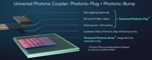
Teramount’s approach
Teramount’s approach couples the fibre to the silicon photonics chip using two components: a photonic plug and a photonic bump.
The photonic plug holds the fibres and couples them to the silicon photonics chip via the photonic bump, a component made during the silicon photonics wafer processing. The photonic bump consists of two elements: a wideband deflector and a lens mirror for beam expansion. Expanding the light beam enables much larger assembly tolerances: +/- 30 microns. And across this 60-micron window, only half a dB is lost in misalignment tolerances.
The resulting wafer-level manufacturing may be more complicated, says Taha, but the benefit is relaxed tolerances in the assembly, wide-band surface coupling, and when testing the wafer and the die.
The photonic bump-and-plug combination also enable detachable optics for co-packaged optics designs. This benefits manufacturing and is wanted for co-packaged optics.
Teraverse and Teraverse-XD
There is a clear demarcation between the optics and the switch chip when using pluggables in the data centre. In contrast, co-packaged optics is a system with the optics embedded alongside the chip. A vendor may work with multiple companies to make co-packaged optics, but one product results, with the chip and optical engined co-packaged.
Teramount’s Teraverse solution, using the plug-and-bump combination, brings pluggability to co-packaged optics. The fibres can be attached and detached from the optical engines. “It’s very important to keep that level of pluggability for co-packaged optics,” says Taha.
The approach also benefits manufacturing yield and testing. Separating the fibres from the package protects the fibres during reflow soldering. “Ideally, you want the fibre connected at the last stage and still maintain high level of testability during the packaging process,” says Taha.
Detachable fibre also brings serviceability to co-packaged optics, benefitting for data centre operators.
Teraverse, Teramount’s detachable fiber-to-chip interface, supports single-mode fiber with 125-micron diameter at a 127-micron pitch separation.

Teraverse-XD, announced for OFC, is a follow-on that doubles the fibre density to achieve a near 64-micron pitch. Here, fibres are placed on top of each other, scaling in the Z-dimension. The approach is like how rods or pipes are stored, with the second row of fibres staggered, sitting in the valleys between adjacent fibers in the lower row.
Two rows of photonic bumps are used to couple the light to each row of fibres (see image above). “It’s very important to keep the same real-estate but to have twice the number of fibres,” says Taha.
Future scaling is possible by adding more rows of fibres or by adopting fibres with a smaller pitch.
Teramount’s technology also supports both edge coupling and surface coupling. “We are agnostic,” says Taha. If a co-packaged optics or optical engine vendor wants to use side coupling, it can use the bump-and-plug combination. The bump deflects the beam upwards to the plug packaging which takes the fibres and sends them out horizontally. “We are converting edge coupling to wideband surface coupling,” says Taha. “You don’t need to sacrifice bandwidth to do surface coupling.”
If the vendor wishes to use a grating coupler, Teramount’s bump-and-plug supports that, too, enabling detachable fibering. But here, only the bump’s expanding mirror is used. “For the wideband surface coupling cased, the bump uses two components: the deflector and the expanding mirror,” says Taha.
Both cases are supported by what Teramount refers to as its Universal Photonic Coupler, shown.
Market expectations
Despite being discussed for over a decade, Taha is not surprised that data centre operators have yet to adopt co-packaged optics.
He points out that hyperscalers only want to use co-packaged optics for Ethernet switches once the technology is more mature. They can also keep using a proven alternative: pluggable modules, that continue to advance.
“Hyperscalers are not against the technology, but it is not mature enough,” says Taha. Hyperscalers and systems vendors also want an established supply chain and not proprietary solutions.
To date, Broadcom’s first co-packaged optics switch solution at 25.6-terabit was adopted by Tencent. Broadcom has announced for OFC that it is now delivering its latest 51.2-terabit Bailly co-packaged optics design, backed by ByteDance.
“AI is a different story,” says Taha. “This is the tipping point for a leading vendor to start taking seriously co-packaged optics.”
The advantage of co-packaged optics here is that it accommodates the reach – radix -as well as power savings and improved latency.
Taha expects initial volumes of co-packaged optics sales in 2026.

A coherent roadmap for co-packaged optics
Is coherent optics how co-packaged will continue to scale? Pilot Photonics certainly thinks so.

Part 1: Co-packaged optics
Frank Smyth, CTO and founder of Pilot Photonics, believes the firm is at an important inflection point.
Known for its comb laser technology, Pilot Photonics has just been awarded a €2.5 million European Innovation Council grant to develop its light-source technology for co-packaged optics.
The Irish start-up is also moving to much larger premises and is on a recruitment drive. “Many of our projects and technologies are maturing,” says Smyth.
Company
Founded in 2011, the start-up spent its early years coupled to Dublin City University. It raised its first notable investment in 2017.
The company began by making lab instrumentation based on its optical comb laser technology which emits multiple sources of light that are frequency- and phased-locked. But a limited market caused the company to pivot, adding photonic integration to its laser know-how.
Now, the start-up has a fast-switching, narrow-linewidth tunable laser, early samples of which are being evaluated by several “tier-one” companies.
Pilot Photonics also has a narrowband indium-phosphide comb laser for optical transport applications. This will be the next product it samples.
More recently, the start-up has been developing a silicon nitride-based comb laser for a European Space Agency project. “The silicon nitride micro-resonator in the comb is a non-linear element that enables a very broad comb for highly parallel communication systems and for scientific applications,” says Smyth. It is this laser type that is earmarked for the data centre and for co-packaged optics applications.
Smyth stresses that while still being a small company, the staff has broad expertise. “We cover the full stack,” he says.
Skills range from epitaxial wafer design, photonic integrated circuit (PIC)s and lasers, radio frequency (RF) and thermal expertise, and digital electronics and control design capabilities.
“We learned early on that it’s all well making a PIC, but if no one can interface to it, you are wasting your time,” says Smyth.
Co-packaged optics
Co-packaged optics refers to adding optics next to an ASIC that has significant input-output (I/O) data requirements. Examples of applications for co-packaged optics include high-capacity Ethernet switch chips and artificial intelligence (AI) accelerators. The goal is to give the chip optical rather than electrical interfaces, providing system-scaling benefits; as electrical signals get faster, their reach shrink.
The industry has been discussing co-packaged optics for over a decade. Switch-chip players and systems vendors have shown prototype designs and even products. And more than half a dozen companies are developing the optical engines that surround, and are packaged with, the chip.
However, the solutions remain proprietary, and while the OIF is working to standardise co-packaged optics, end users have yet to embrace the technology. In part, this is because pluggable optical modules continue to advance in data speeds and power consumption, with developments like linear-drive optics.
The ecosystem supporting co-packaged optics is also developing. Hyperscalers will only deploy co-packaged optics in volume when reliability and a broad manufacturing base are proven.
Yet industry consensus remains that optical I/O is a critical technology and that deployments will ramp up in the next two years. Ethernet switch capacity doubles every two years while AI accelerator chips are progressing rapidly. Moreover, the number of accelerator chips used in AI supercomputers is growing fast, from thousands to tens of thousands.
Pilot Photonics believes its multi-wavelength laser technology, coupled with the intellectual property it is developing, will enable co-packaged optics based on coherent optics to address such scaling issues.
Implementations
Co-packaged optics uses optical chiplets or ‘engines’ that surround the ASIC on a shared substrate. The optical engines typically use an external laser source although certain co-packaged optics solutions such as from Intel and Ranovus can integrate the laser as part of the silicon-photonics based optical engine.
Designers can scale the optical engine’s I/O capacity in several ways. They can increase the number of fibres connected to the optical engine, send more wavelengths down each fibre, and increase the wavelength’s data rate measured in gigabits per second (Gbps).
In co-packaged optics designs, 16 engines typically surround the chip. For a 25.6-terabit Ethernet chip, 16 x 1.6-terabit engines are used, each 1.6-terabit engine sending a 100Gbps DR1 signal per fibre. The total fibres per engine equals 32: 16 for the transmit and 16 for the receive (see table).
| Switch capacity/Tbps | Optical engine/Tbps | Optical engines | Data rate/fibre | No. fibres/ engine* |
| 25.6 | 1.6 | 16 | 100G DR, 500m | 32 |
| 25.6 | 3.2 | 8 | 100G DR, 500m | 64 |
| 51.2 | 6.4 | 8 | 400G FR4, 2km | 32 |
| 102.4 (speculative) | 6.4 | 16 | 400G FR4, 2km | 16 |
| 102.4 (speculation) | 12.8 | 8 | 400G FR4, 2km | 32 |
*Not counting the external laser source fibre.
Broadcom’s co-packaged optical approach uses eight optical engines around its 25.6-terabit Tomahawk 4 switch chip, each with 3.2Tbps capacity. For the Tomahawk 5, 51.2-terabit Bailly co-packaged optics design, Broadcom uses eight, 6.4Tbps optical engines, sending 400-gigabit FR4, or 4-wavelength coarse WDM wavelengths, across each fibre. Using FR4 instead of DR1 halves the number of optical engines while doubling overall capacity.
The co-packaging solutions used in the next-generation 102.4-terabit switch chip are still to be determined. Capacity could be doubled using twice as many fibres, or by using 200-gigabit optical wavelengths based on 112G PAM-4 electrical inputs, twice the speed currently used.
But scaling routes for the generation after that – 204.8-terabit switch chips and beyond – and the co-packaged optics design become unclear due to issues of dispersion and power constraints, says Smyth.
Scaling challenges
Assuming eight engines were used alongside the 200-terabit ASIC , each would need to be 25.6Tbps. The fibre count per engine could be doubled again or more wavelengths per fibre would be needed. One player, Nubis Communications, scales its engines and fibres in a 2D array over the top of the package, an approach suited to fibre-count growth.
Doubling the wavelength count is another option but adopting an 8-wavelength CWDM design with 20nm spacing means the wavelengths would cover 160nm of spectrum. Over a 2km reach, this is challenging due to problems with dispersion. Narrower channel spacings such as those used in the CW-WDM MSA (multi-source agreement) require temperature control to ensure the wavelengths stay put.
Keeping the symbol rate fixed but doubling the data rate is another option. But adopting the more complex PAM-8 modulation brings its own link challenges.
Another key issue is power. Current 51.2-terabit switches require 400mW of laser launch power (4 x 100mW lasers) per fibre and there are 128 transmit fibers per switch.
“Assuming a wall plug efficiency of 20 per cent, that is around 250W of power dissipation just for the lasers,” says Smyth. “Getting to 4Tbps per fibre appears possible using 16 wavelengths, but the total fiber launch power is 10 times higher, requiring 2.5kW of electrical power per switch just for the lasers.”
In contrast, single-polarisation coherent detection of 16-QAM signals through a typical path loss of 24dB could match that 4Tbps capacity with the original 250W of laser electrical power, he says.
 The optimised total laser power improvement for coherent detection versus direct detection as a function of the additional losses in the signal path (the losses not also experienced by the local oscillator). Source: Pilot Photonics
Coherent detection is associated with a high-power digital signal processor (DSP). Are such chips feasible for such a power-sensitive application as co-packaged optics?
Coherent detection adds some DSP complexity, says Smyth, but it has been shown that for pluggable-based intra data centre links using 5nm CMOS silicon, 400-gigabit coherent and direct-detection are comparable in terms of ASIC power but coherent requires less laser power.
“Over time, a similar battle will play out for co-packaged optics. Laser power will become a bigger issue than DSP power,” he says.
The additional signal margin could be used for 10km links, with tens of terabits per fibre and even 80km links at similar per-fibre rates to current direct detection.
“We believe coherent detection in the data centre is inevitable,” says Smyth. “It’s just a question of when.”
Comb-based coherent co-packaged optics
Coherent co-packaged optics brings its own challenges. Coherent detection requires alignment between the signal wavelength and the local oscillator laser in the receiver. Manufacturing tolerances and the effects of ageing in simple laser arrays make this challenging to achieve.
“The wavelengths of a comb laser are precisely spaced, which greatly simplifies the problem,” says Smyth. “And combs bring other benefits related to carrier recovery and lack of inter-channel interference too”.
Pilot Photonics’ comb laser delivers 16 or 32 wavelengths per fibre, up to 8x more than existing solutions. Smyth says the company intends to fit its comb laser inside the OIF’s standardised External Laser Source pluggable form-factor,
The start-up is also developing a coherent ring resonator modulator for its design. The ring modulator is tiny compared with Mach-Zehnder interferometer modulators used for coherent optics.
Pilot Photonics is also developing IP for coherent signal processing. Because its comb laser locks the frequency and phase of the wavelengths generated, the overall control and signal processing can be simplified.
While it will offer the comb laser, the start-up does not intend to develop the DSP IC nor make optical engines itself.
“A strategic partnership with a company with its own manufacturing facilities would be the most effective way of getting this technology to market,” says Smyth.