
ST makes its first PSM4 optical engine deliveries
What gives Benetti confidence is the demand he is seeing for 100-gigabit transceivers in the data centre. “From my visibility today, the tipping point is 2016,” says Benetti, group vice president and general manager, digital and mixed processes ASIC division at STMicroelectronics.
 Flavio Benetti
Benetti and colleagues at ST have spent the last four years working to bring to market the silicon photonics technology that the chip company licensed from Luxtera.
The company has developed a 300mm-wafer silicon photonics production line at its fabrication plant in Crolles that is now up and running. ST also has its first silicon photonics product - a mid-reach PSM4 100-gigabit optical engine - and has just started its very first deliveries.
At the OFC show in March, ST said it had already delivered samples to one unnamed 'customer partner', possibly Luxtera, and Benetti showed a slide of the PSM4 chips as part of a Lumentum transceiver.
Another ST achievement Benetti highlights is the development of a complete supply chain for the technology. In addition to wafer production, ST has developed electro-optic wafer testing. This allows devices to be probed electrically and optically to select working designs before the wafer is diced. ST has also developed a process to 3D-bond chips.
“We have focussed on building an industrial environment, with a supply chain that can deliver hundreds of thousands and millions of devices,” says Benetti.
PSM4 and CWDM4
ST’s first product, the components for a 4x25 gigabit PSM4 transceiver, is a two-chip design.
One chip is the silicon photonics optical engine which integrates the PSM4’s four modulators, four detectors and the grating couplers used to interface the chip to the fibres. The second chip, fabricated using ST’s 55nm BiCMOS process, houses the transceiver’s associated electronics such as the drivers, and trans-impedance amplifiers.
The two chips are combined using 3D packaging. “The 3D packaging consists of the two dies, one copper-pillar bonded to the other,” says Benetti. “It is a dramatic simplification of the mounting process of an optical module.”
The company is also developing a 100-gigabit CWDM4 transceiver which unlike the PSM4 uses four 25-gigabit wavelengths on a single fibre.
The CWDM4 product will be developed using two designs. The first is an interim, hybrid solution that uses an external planar lightwave circuit-based multiplexer and demultiplexer, followed by an integrated silicon photonics design. The hybrid design is being developed and is expected in late 2017; the integrated silicon photonics design is due in 2018.
With the hybrid design, it is not just a question of adding a mux-demux to the PSM4 design. “The four channels are each carrying a different wavelength so there are some changes that need to be done to the PSM4,” says Benetti, adding that ST is working with partners that will provide the mux-demux and do the integration.
We need to have a 100-gigabit solution in high volume for the market, and the pricing pressure that is coming has convinced us that silicon photonics is the right thing to do
Opportunities
Despite the growing demand for 100-gigabit transceivers that ST is seeing, Benetti stresses that these are not 'mobile-phone wafer volumes'. “We are much more limited in terms of wafers,” he says. Accordingly, there is probably only room for one or two large fabs for silicon photonics globally, in his opinion.
So why is ST investing in a large production line? For Benetti, this is an obvious development for the company which has been a provider of electrical ICs for the optical module industry for years.
“ST has entered silicon photonics to provide our customers with a roadmap,” says Benetti. “We need to have a 100-gigabit solution in high volume for the market, and the pricing pressure that is coming has convinced us that silicon photonics is the right thing to do.”
It also offers chip players the possibility of increasing its revenues. “The optical engine integrates all the components that were in the old-fashioned modules so we can increase our revenues there,” he says.
ST is tracking developments for 200-gigabit and 400-gigabit links and is assessing whether there is enough of an opportunity to justify pursuing 200-gigabit interconnects.
For now though, it is seeing strong pricing pressure for 100-gigabit links for reaches of several hundred meters. “We do not think we can compete for very short reach distances,” says Benetti. “We will leave that to VCSELs until the technology can no longer follow.” As link speeds increase, the reach of VCSEL links diminishes. “We will see more room for silicon photonics but this is not the case in the short term,” says Benetti.
Market promise
People have been waiting for years for silicon photonics to become a reality, says Benetti. “My target is to demonstrate it [silicon photonics] is possible, that we are serious in delivering parts to the market in an industrial way and in volumes that have not been delivered before.”
To convince the market, it is not just showing the technological advantages of silicon photonics but the fact that there is a great simplification in constructing the optical module along with the ability to deliver devices in volume. “This is the point,” he says.
Benetti’s other role at ST is overseeing advanced networking ASICs. He argues that over the mid- to long-term, there needs to be a convergence between ASIC and optical connectivity.
“Look at a switch board, for example, you have a big ASIC or two in the middle and a bunch of optical modes on the side,” says Benetti. For him, the two technologies - photonics and ICs - are complementary and the industry’s challenge is to make the two live together in an efficient way.
FPGAs with 56-gigabit transceivers set for 2017
The company demonstrated a 56-gigabit transceiver using 4-level pulse-amplitude modulation (PAM-4) at the recent OFC show. The 56-gigabit transceiver, also referred to as a serialiser-deserialiser (serdes), was shown successfully working over backplane specified for 25-gigabit signalling only.
 Gilles GarciaXilinx's 56-gigabit serdes is implemented using a 16nm CMOS process node but the first FPGAs featuring the design will be made using a 7nm process. Gilles Garcia says the choice of 7nm CMOS is solely a business decision and not a technical one.
”Optical module [makers] will take another year to make something decent using PAM-4," says Garcia, Xilinx's director marketing and business development, wired communications. "Our 7nm FPGAs will follow very soon afterwards.”
The company is still to detail its next-generation FPGA family but says that it will include an FPGA capable of supporting 1.6 terabit of Optical Transport Network (OTN) using 56-gigabit serdes only. At first glance that implies at least 28 PAM-4 transceivers on a chip but OTN is a complex design that is logic not I/O limited suggesting that the FPGA will feature more than 28, 56-gigabit serdes.
Applications
Xilinx’s Virtex UltraScale and its latest UltraScale+ FPGA families feature 16-gigabit and 25-gigabit transceivers. Managing power consumption and maximising reach of the high-speed serdes are key challenges for its design engineers. Xilinx says it has 150 engineers for serdes design.
“Power is always a key challenge because as soon as you talk about 400-gigabit to 1-terabit per line card, you need to be cautious about the power your serdes will use,” says Garcia. He says the serdes need to adapt to the quality of the traces for backplane applications. Customers want serdes that will support 25 gigabit on existing 10-gigabit backplane equipment.
Xilinx describes its Virtex UltraScale as a 400-gigabit capable single-chip system supporting up to 104 serdes: 52 at 16 gigabit and 52 at 25 gigabit.
The UltraScale+ is rated as a 500-gigabit to 600-gigabit capable system, depending on the application. For example, the FPGA could support three, 200-gigabit OTN wavelengths, says Garcia.
Xilinx says the UltraScale+ reduces power consumption by 35% to 50% compared to the same designs implemented on the UltrasScale. The Virtex UltraScale+ devices also feature dedicated hardware to implement RS-FEC, freeing up programmable logic for other uses. RS-FEC is used with multi-mode fibre or copper interconnects for error correction, says Xilinx. Six UltraScale+ FPGAs are available and the VU13P, not yet out, will feature up to 128 serdes, each capable of up to 32 gigabit.
We don’t need retimers so customers can connect directly to the backplane at 25 gigabit, thereby saving space, power and cost
The UltraScale and UltraScale+ FPGAs are being used in several telecom and datacom applications.
For telecom, 500-gigabit and 1-terabit OTN designs are an important market for the UltraScale FPGAs. Another use for the FPGA serdes is for backplane applications. “We don’t need retimers so customers can connect directly to the backplane at 25 gigabit, thereby saving space, power and cost,” says Garcia. Such backplane uses include OTN platforms and data centre interconnect systems.
The FPGA family’s 16-gigabit serdes are also being used in 10-gigabit PON and NG-PON2 systems. “When you have an 8-port or 16-port system, you need to have a dense serdes capability to drive the [PON optical line terminal’s] uplink,” says Garcia.
For data centre applications, the FPGAs are being employed in disaggregated storage systems that involved pooled storage devices. The result is many 16-gigabit and 25-gigabit streams accessing the storage while the links to the data centre and its servers are served using 100-gigabit links. The FPGA serdes are used to translate between the two domains (see diagram).
 Source: Xilinx
For its next-generation 7nm FPGAs with 56-gigabit transceivers, Xilinx is already seeing demand for several applications.
Data centre uses include server-to-top-of-rack links as the large Internet providers look move from 25 gigabit to 50- and 100-gigabit links. Another application is to connect adjacent buildings that make up a mega data centre which can involve hundreds of 100-gigabit links. A third application is meeting the growing demands of disaggregated storage.
For telecom, the interest is being able to connect directly to new optical modules over 50-gigabit lanes, without the need for gearbox ICs.
Optical FPGAs
Altera, now part of Intel, developed an optical FPGA demonstrator that used co-packaged VCSELs for off-chip optical links. Since then Altera announced its Stratix 10 FPGAs that include connectivity tiles - transceiver logic co-packaged and linked with the FPGA using interposer technology.
Xilinx says it has studied the issue of optical I/O and that there is no technical reason why it can’t be done. But the issue is a business one when integrating optics in an FPGA, he says: “Who is responsible for the yield? For the support?”
Garcia admits Xilinx could develop its own I/O designs using silicon photonics and then it would be responsible for the logic and the optics. “But this is not where we are seeing the business growing,” he says.
Enabling coherent optics down to 2km short-reach links
Interview 5: Chris Doerr
Chris Doerr admits he was a relative latecomer to silicon photonics. But after making his first silicon photonics chip, he was hooked. Nearly a decade later and Doerr is associate vice president of integrated photonics at Acacia Communications. The company uses silicon photonics for its long-distance optical coherent transceivers.
 Chris Doerr in the lab
Acacia Communications made headlines in May after completing an initial public offering (IPO), raising approximately $105 million for the company. Technology company IPOs have become a rarity and are not always successful. On its first day of trading, Acacia’s shares opened at $29 per share and closed just under $31.
Although investors may not have understood the subtleties of silicon photonics or coherent DSP-ASICs for that matter, they noted that Acacia has been profitable since 2013. But as becomes clear in talking to Doerr, silicon photonics plays an important role in the company’s coherent transceiver design, and its full potential for coherent has still to be realised.
Bell Labs
Doerr was at Bell Labs for 17 years before joining Acacia in 2011. He spent the majority of his time at Bell Labs making first indium phosphide-based optical devices and then also planar lightwave circuits. One of his bosses at Bell Labs was Y.K. Chen. Chen had arranged a silicon photonics foundry run and asked Doerr if he wanted to submit a design.
What hooked Doerr was silicon photonics’ high yields. He could assume every device was good, whereas when making complex indium phosphide designs, he would have to test maybe five or six devices before finding a working one. And because the yields were high, he could focus more on the design aspects. “Then you could start to make very complex designs - devices with many elements - with confidence,” he says.
Another benefit was that the performance of the silicon photonic circuit matched closely its simulation results. “Indium phosphide is so complex,” he says. “You have to worry about the composition effects and the etching is not that precise.” With silicon, in contrast, the dimensions and the refractive index are known with precision. “You can simulate and design very precisely, which made it [the whole process] richer,” says Doerr.
Silicon photonics is a disruptive technology because of its ability to integrate so many things together and still be high yield and get the raw performance
After that first wafer run, Doerr continued to design both planar lightwave circuits and indium phosphide components at Bell Labs. But soon it was solely silicon photonics ICs.
Doerr views Acacia’s volume production of an integrated coherent transceiver - the transmit and receive optics on the one chip - with a performance that matches discrete optical designs, as one of silicon photonics’ most notable achievements to date.
With a discrete component coherent design, you can use the best of each material, he explains, whereas with an integrated design, compromises are inevitable. “You can’t optimise the layer structure; each component has to share the wafer structure,” he says. Yet with silicon photonics, the design space is so powerful and high-yielding, that these compromises are readily overcome.
Doerr also describes a key moment when he realised the potential of silicon photonics for volume manufacturing.
He was reading an academic paper on grating couplers, a structure used to couple fibres to waveguides. “You can only make that in silicon photonics because you need a high vertical [refractive] index contrast,” he says. Technically, a grating coupler can also be made in indium phosphide but the material has to be cut from under the waveguide; this leaves the waveguide suspended in air.
When he first heard of grating couplers he assumed the coupling efficiency would be of the order of a few percent whereas in practice it is closer to 85 percent. “That is when I realised it is a very powerful concept,” he says.
Integration is key
Doerr pauses before giving measured answers to questions about silicon photonics. Nor does his enthusiasm for silicon photonics blinker him to the challenges it faces. However, his optimism regarding the technology’s future is clear.
“Silicon photonics is a disruptive technology because of its ability to integrate so many things together and still be high yield and get the raw performance,” he says. In the industry, silicon photonics has proven itself for such applications as metro telecommunications but it faces significant competition from established technologies such as indium phosphide. It will require more channels to be integrated for the full potential of silicon photonics as a disruption technology to emerge, says Doerr.
Silicon photonics also has an advantage on indium phosphide in that it can be integrated with electronic ICs using 2.5D and 3D packaging, saving cost, footprint, and power. “If you are in the same material system then such system-in-package is easier,” he says. Also, silicon photonic integrated circuits do not require temperature control, unlike indium phosphide modulators, which saves power.
Areas of focus
One silicon photonics issue is the need for an external laser. For coherent transceivers, it is better to separate the laser from the high-speed optics due to the fact that the coherent DSP-ASIC and the photonic chips are hot and the laser requires temperature control.
For applications such as very short reach links, silicon photonics needs a laser source and while there are many options to integrate the laser to the chip, a clear winning approach has yet to emerge. “Until a really low cost solution is found, it precludes silicon from competing with really low-cost solutions like VCSELs for very short reach applications,” he says.
Silicon photonic chip volumes are still many orders of magnitude fewer than those of electronic ICs. But Acacia says foundries already have silicon photonics lines running, and as these foundries ramp volumes, costs, production times, and node-sizes will continually improve.
Opportunities
The adoption of silicon photonics will increase significantly as more and more functions are integrated onto devices. For coherent designs, Doerr can foresee silicon photonics further reducing the size, cost and power consumption, making them competitive with other optical transceiver technologies for distances as short as 2km.
“You can use high-order formats such as 256-QAM and achieve very high spectral efficiency,” says Doerr. Using such a modulation scheme would require fewer overall lasers to achieve significant transport capacities, improving the cost-per-bit performance for applications such as data centre interconnect. “Fibre is expensive so the more you can squeeze down a fibre, the better,” he says.
Doerr also highlights other opportunities for silicon photonics, beyond communications. Medical applications is one such area. He cites a post-deadline paper at OFC 2016 from Acacia on optical coherent tomography which has similarities with the coherent technology used in telecom.
Longer term, he sees silicon photonics enabling optical input/ output (I/O) between chips. As further evolutionary improvements are achieved, he can see lasers being used externally to the chip to power such I/O. “That could become very high volume,” he says.
However, he expects 3D stacking of chips to take hold first. “That is the easier way,” he says.
NeoPhotonics showcases a CFP2-ACO roadmap to 400G
The company demonstrated the CFP2-ACO module transmitting at 100 gigabit using polarisation multiplexed, quadrature phase-shift keying (PM-QPSK) modulation at the recent OFC show. The line-side module is capable of transmitting over 1,000km and also supports PM-16QAM that doubles capacity over metro network distances.
 Ferris LipscombThe CFP2-ACO is a Class 3 design: the control electronics for the modulator and laser reside on the board, alongside the coherent DSP-ASIC chip.
At OFC, NeoPhotonics also demonstrated single-wavelength 400-gigabit transmission using more advanced modulation and a higher symbol rate, and a short-reach 100-gigabit link for inside the data centre using 4-level pulse-amplitude modulation (PAM4) signalling.
Roadmap to 400 gigabit
One benefit of the CFP2-ACO is that the pluggable module can be deployed only when needed. Another is that the optics will work with coherent DSP-ASICs for different systems vendors and merchant chip suppliers.
“After a lot of technology-bragging about the CFP2-ACO, this is the year it is commercial,” says Ferris Lipscomb, vice president of marketing at NeoPhotonics.
Also demonstrated were the components needed for a next-generation CFP2-ACO: NeoPhotonics’ narrow line-width tunable laser and its higher-bandwidth integrated coherent receiver. To achieve 400 gigabit, 32-QAM and a 45 gigabaud symbol rate were used.
Traditional 100-gigabit coherent uses a 32-gigabaud symbol rate. That combined with QPSK and the two polarisations results in a total bit rate of 2 polarisations x 2bits/symbol x 32 gigabaud or 128 gigabits: a 100-gigabit payload and the rest overhead bits. Using 32-QAM instead of QPSK increases the number of bits encoded per symbol from 2 to 5, while increasing the baud rate from 32 to 45 gigabaud adds a speed-up factor of 1.4. Combining the two, the resulting bit rate is 45 gigabaud x 5bits/symbol x 2 polarisations or 450 gigabit overall.
After a lot of technology-bragging about the CFP2-ACO, this is the year it is commercial
Using 32-QAM curtails the transmission distance to 100km due to the denser constellation but such distances are suited for data centre interconnect applications.
“That was the demo [at OFC] but the product is also suitable for metro distances of 500km using 16-QAM and long-haul of 1,000km using 200 gigabit and 8-QAM,” says Lipscomb.
PAM4
The PAM4 demonstration highlighted NeoPhotonics’ laser and receiver technology. The company showcased a single-wavelength link running at 112 gigabits-per-second using its 56Gbaud externally modulated laser (EML) with an integrated driver. The PAM4 link can span 2km in a data centre.
“What is not quite ready for building into modules is the [56Gbaud to 112 gigabit PAM4] DSP, which is expected to be out in the middle to the second half of the year,” says Lipscomb. The company will develop its own PAM4-based optical modules while selling its laser to other module makers.
Lipscomb says four lanes at 56 gigabaud using PAM4 will deliver a cheaper 400-gigabit solution than eight lanes, each at 25 gigabaud.
Silicon Photonics
NeoPhotonics revealed that it is supplying new 1310nm and 1550nm distributed feedback (DFB) lasers to optical module players that are using silicon photonics for their 100-gigabit mid-reach transceivers. These include the 500m PSM-4, and the 2km CWDM4 and CLR4.
Lipscomb says the benefits of its lasers for silicon photonics include their relatively high output power - 40 to 60mW - and the fact that the company also makes laser arrays which are useful for certain silicon photonics applications.
NeoPhotonics’ laser products have been for 100-gigabit modules with reaches of 2km to 10km. “Silicon photonics is usually used for shorter reaches of a few hundred meters,” says Lipscomb. “This new product is our first one aimed at the short reach data centre market segment.”
“Our main products have been for 100-gigabit modules for the longer reaches of 2km to 10km,” says Lipscomb. “Silicon photonics is usually used for shorter reaches of a few hundred meters, and this new [laser] product is our first one aimed at the short reach data centre market segment."
The company says it has multiple customer engagements spanning various wavelength plans and approaches for Nx100-gigabit data centre transceiver designs. Mellanox Technologies is one vendor using silicon photonics that NeoPhotonics is supplying.
The white box concept gets embraced at the optical layer
 Brandon Collings
White boxes have arisen to satisfy the data centre operators’ need for simple building-block functions in large number that they can direct themselves.
“They [data centre operators] started using very simple white boxes - rather simple functionality, much simpler than the large router companies were providing - which they controlled themselves using software-defined networking orchestrators,” says Brandon Collings, CTO of Lumentum.
Such platforms have since evolved to deliver high-performance switching, controlled by third-party SDN orchestrators, and optimised for the simple needs of the data centre, he says. Now this trend is moving to the optical layer where the same flexibility of function is desired. Operators would like to better pair the functionality that they are going to buy with the exact functionality they need for their network, says Collings.
“There is no plan to build networks with different architectures to what is built today,” he says. “It is really about how do we disaggregate conventional platforms to something more flexible to deploy, to control, and which you can integrate with control planes that also manage higher layers of the network, like OTN and the packet layer.”
White box products
Lumentum has a background in integrating optical functions such as reconfigurable optical add/drop multiplexers (ROADMs) and amplifiers onto line cards, known as its TrueFlex products. “That same general element is now the element being demanded by these white box strategies, so we are putting them in pizza boxes,” says Collings.
At OFC, Lumentum announced several white box designs for linking data centres and for metro applications. Such designs are for large-scale data centre operators that use data centre interconnect platforms. But several such operators also have more complex, metro-like optical networking requirements. Traditional telcos such as AT&T are also interested in pursuing the approach.
The first Lumentum white box products include terminal and line amplifiers, a dense WDM multiplexer/ demultiplexer and a ROADM. These hardware boxes come with open interfaces so that they can be controlled by an SDN orchestrator and are being made available to interested parties.
OpenFlow, which is used for electrical switches in the data centre, could be use with such optical white boxes. Other more likely software are the Restconf and Netconf protocols. “They are just protocols that are being defined to interface the orchestrator with a collection of white boxes,” says Collings.
Lumentum’s mux-demux is defined as a white box even though it is passive and has no power or monitoring requirements. That is because the mux-demux is a distinct element that is not part of a platform.
AT&T is exploring the concept of a disaggregated ROADM. Collings says a disaggregated ROADM has two defining characteristics. One is that the hardware isn’t required to come with a full network control management system. “You can buy it and operate it without buying that same vendor’s control system,” he says. The second characteristic is that the ROADM is physically disaggregated - it comes in a pizza box rather than a custom, proprietary chassis.
There remains a large amount of value between encompassing optical hardware in a pizza box to delivering an operating network
Lumentum: a systems vendor?
The optical layer white box ecosystem continues to develop, says Collings, with many players having different approaches and different levels of ‘aggressiveness’ in pursuing the concept. There is also the issue of the orchestrators and who will provide them. Such a network control system could be written by the hyper-scale data centre operators or be developed by the classical network equipment manufacturers, says Collings.
Collings says selling pizza boxes does not make Lumentum a systems vendor. “There is a lot of value-add that has to happen between us delivering a piece of hardware with simple open northbound control interfaces and a complete deployed, qualified, engineered system.”
Control software is needed as is network engineering; value that traditional system vendors have been adding. “That is not our expertise; we are not trying to step into that space,” says Collings. There remains a large amount of value between encompassing optical hardware in a pizza box to delivering an operating network, he says.
This value and how it is going to be provided is also at the core of an ongoing industry debate. “Is it the network provider or the people that are very good at it: the network equipment makers, and how that plays out.”
Lumentum’s white box ROADM was part of an Open Networking Lab proof-of-concept demonstration at OFC.
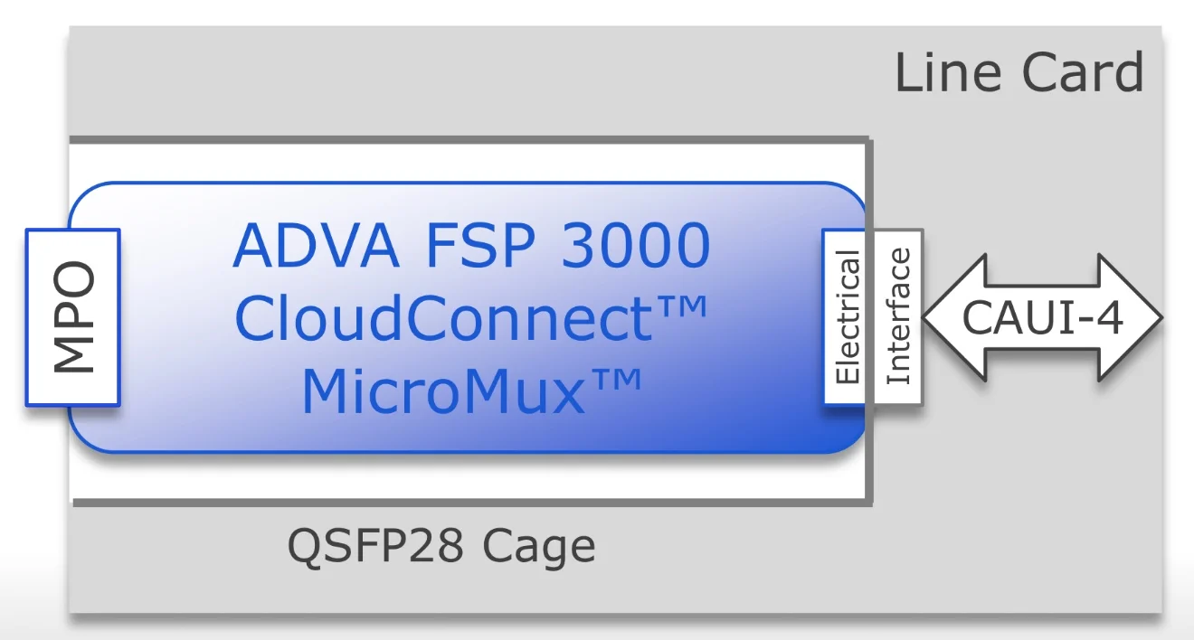
QSFP28 MicroMux expands 10 & 40 Gig faceplate capacity
- ADVA Optical Networking's MicroMux aggregates lower rate 10 and 40 gigabit client signals in a pluggable QSFP28 module
- ADVA is also claiming an industry first in implementing the Open Optical Line System concept that is backed by Microsoft
The need for terabits of capacity to link Internet content providers’ mega-scale data centres has given rise to a new class of optical transport platform, known as data centre interconnect.
 Source: ADVA Optical Networking
Such platforms are designed to be power efficient, compact and support a variety of client-side signal rates spanning 10, 40 and 100 gigabit. But this poses a challenge for design engineers as the front panel of such platforms can only fit so many lower-rate client-side signals. This can lead to the aggregate data fed to the platform falling short of its full line-side transport capability.
ADVA Optical Networking has tackled the problem by developing the MicroMux, a multiplexer placed within a QSFP28 module. The MicroMux module plugs into the front panel of the CloudConnect, ADVA’s data centre interconnect platform, and funnels either 10, 10-gigabit ports or two, 40-gigabit ports into a front panel’s 100-gigabit port.
"The MicroMux allows you to support legacy client rates without impacting the panel density of the product," says Jim Theodoras, vice president of global business development at ADVA Optical Networking.
Using the MicroMux, lower-speed client interfaces can be added to a higher-speed product without stranding line-side bandwidth. An alternative approach to avoid wasting capacity is to install a lower-speed platform, says Theodoras, but then you can't scale.
ADVA Optical Networking offers four MicroMux pluggables for its CloudConnect data centre interconnect platform: short-reach and long-reach 10-by-10 gigabit QSFP28s, and short-reach and intermediate-reach 2-by-40 gigabit QSFP28 modules.
The MicroMux features an MPO connector. For the 10-gigabit products, the MPO connector supports 20 fibres, while for the 40-gigabit products, it is four fibres. At the other end of the QSFP28, that plugs into the platform, sits a CAUI-4 4x25-gigabit electrical interface (see diagram above).
“The key thing is the CAUI-4 interface; this is what makes it all work," says Theodoras.
Inside the MicroMux, signals are converted between the optical and electrical domains while a gearbox IC translates between 10- or 40-gigabit signals and the CAUI-4 format.
Theodoras stresses that the 10-gigabit inputs are not the old 100 Gigabit Ethernet 10x10 MSA but independent 10 Gigabit Ethernet streams. "They can come from different routers, different ports and different timing domains," he says. "It is no different than if you had 10, 10 Gigabit Ethernet ports on the front face plate."
Using the pluggables, a 5-terabit CloudConnect configuration can support up to 520, 10 Gigabit Ethernet ports, according to ADVA Optical Networking.
The first products will be shipped in the third quarter to preferred customers that help in its development while the products will be generally available at the year-end.
ADVA Optical Networking unveiled the MicroMux at OFC 2016, held in Anaheim, California in March. ADVA also used the show to detail its Open Optical Line System demonstration with switch vendor, Arista Networks.
Two years after Microsoft first talked about the [Open Optical Line System] concept at OFC, here we are today fully supporting it
Open Optical Line System
The Open Optical Line System is a concept being promoted by the Internet content providers to afford them greater control of their optical networking requirements.
Data centre players typically update their servers and top-of-rack switches every three years yet the optical transport functions such as the amplifiers, multiplexers and ROADMs have an upgrade cycle closer to 15 years.
“When the transponding function is stuck in with something that is replaced every 15 years and they want to replace it every three years, there is a mismatch,” says Theodoras.
Data centre interconnect line cards can be replaced more frequently with newer cards while retaining the chassis. And the CloudConnect product is also designed such that its optical line shelf can take external wavelengths from other products by supporting the Open Optical Line System. This adds flexibility and is done in a way that matches the work practices of the data centre players.
“The key part of the Open Optical Line System is the software,” says Theodoras. “The software lets that optical line shelf be its own separate node; an individual network element.”
The data centre operator can then manage the standalone CloudConnect Open Optical Line System product. Such a product can take coloured wavelength inputs and even provide feedback with the source platform, so that the wavelength is tuned to the correct channel. “It’s an orchestration and a management level thing,” says Theodoras.
Arista recently added a coherent line card to its 7500 spine switch family.
The card supports six CFP2-ACOs that have a reach of up to 2,000km, sufficient for most data centre interconnect applications, says Theodoras. The 7500 also supports the layer-two MACsec security protocol. However, it does not support flexible modulation formats. The CloudConnect does, supporting 100-, 150- and 200-gigabit formats. CloudConnect also has a 3,000km reach.
 Source: ADVA Optical Networking
In the Open Optical Line System demonstration, ADVA Optical Networking squeezed the Arista 100-gigabit wavelength into a narrower 37.5GHz channel, sandwiched between two 100 gigabit wavelengths from legacy equipment and two 200 gigabit (PM-16QAM) wavelengths from the CloudConnect Quadplex card. All five wavelengths were sent over a 2,000km link.
Implementing the Open Optical Line System expands a data centre manager’s options. A coherent card can be added to the Arista 7500 and wavelengths sent directly using the CFP2-ACOs, or wavelengths can be sent over more demanding links, or ones that requires greater spectral efficiency, by using the CloudConnect. The 7500 chassis could also be used solely for switching and its traffic routed to the CloudConnect platform for off-site transmission.
Spectral efficiency is important for the large-scale data centre players. “The data centre interconnect guys are fibre-poor; they typically only have a single fibre pair going around the country and that is their network,” says Theodoras.
The joint demo shows that the Open Optical Line System concept works, he says: “Two years after Microsoft first talked about the concept at OFC, here we are today fully supporting it.”
Infinera goes multi-terabit with its latest photonic IC
In his new book, The Great Acceleration, Robert Colvile discusses how things we do are speeding up.
In 1845 it took U.S. President James Polk six months to send a message to California. Just 15 years later Abraham Lincoln's inaugural address could travel the same distance in under eight days, using the Pony Express. But the use of ponies for transcontinental communications was shortlived once the electrical telegraph took hold. [1]
The relentless progress in information transfer, enabled by chip advances and Moore's law, is taken largely for granted. Less noticed is the progress being made in integrated photonic chips, most notably by Infinera.
In 2000, optical transport sent data over long-haul links at 10 gigabit-per-second (Gbps), with 80 such channels supported in a platform. Fifteen years later, Infinera demonstrated its latest-generation photonic integrated circuit (PIC) and FlexCoherent DSP-ASIC that can transmit data at 600Gbps over 12,000km, and up to 2.4 terabit-per-second (Tbps) - three times the data capacity of a state-of-the-art dense wavelength-division multiplexing (DWDM) platform back in 2000 - over 1,150km.
Infinite Capacity Engine
Infinera dubs its latest optoelectronic subsystem the Infinite Capacity Engine. The subsystem comprises a pair of indium-phosphide PICs - a transmitter and a receiver - and the FlexCoherent DSP-ASIC. The performance capabilities that the Infinite Capacity Engine enables were unveiled by Infinera in January with its Advanced Coherent Toolkit announcement. Now, to coincide with OFC 2016, Infinera has detailed the underlying chips that enable the toolkit. And company product announcements using the new hardware will be made later this year, says Pravin Mahajan, the company's director of product and corporate marketing.
The claimed advantages of the Infinite Capacity Engine include a 82 percent reduction in power consumption compared to a system using discrete optical components and a dozen 100-gigabit coherent DSP-ASICs, and a 53 percent reduction in total-cost-of-ownership compared to competing dense WDM platforms. The FlexCoherent chip also features line rate data encryption.
"The Infinite Capacity Engine is the industry's first multi-terabit it super-channel, says Mahajan. "It also delivers the industry's first multi-terabit layer one encryption."
Multi-terabit PIC
Infinera's first transmitter and receiver PIC pair, launched in 2005, supported 10, 10-gigabit channels and implemented non-coherent optical transmission.
In 2011 Infinera introduced a 500-gigabit super-channel coherent PIC pair used with Infinera's DTN-X platforms and also its Cloud Xpress data centre interconnect platform launched in 2014. The 500 Gigabit design implemented 10, 50 gigabit channels that implemented polarisation-multiplexed, quadrature phase-shift keying (PM-QPSK) modulation. The accompanying FlexCoherent DSP-ASIC was implemented using a 40nm CMOS process node and support a symbol rate of 16 gigabaud.
The PIC design has since been enhanced to also support additional modulation schemes such as as polarisation-multiplexed, binary phase-shift keying (PM-BPSK) and 3 quadrature amplitude modulation (PM-3QAM) that extend the DTN-X's ultra long-haul performance.
In 2015 Infinera also launched the oPIC-100, a 100-gigabit PIC for metro applications that enables Infinera to exploit the concept of sliceable bandwidth by pairing oPIC-100s with a 500 gigabit PIC. Here the full 500 gigabit super-channel capacity can be pre-deployed even if not all of the capacity is used. Using Infinera's time-based instant bandwidth feature, part of that 500 gigabit capacity can be added between nodes in a few hours based on a request for greater bandwidth.
Now, with the Infinite Capacity Engine PIC, the effective number of channels has been expanded to 12, each capable of supporting a range of modulation techniques (see table below) and data rates. In fact, Infinera uses multiple Nyquist sub-carriers spread across each of the 12 channels. By encoding the data across multiple sub-carriers a lower-baud rate can be used, increasing the tolerance to non-linear channel impairments during optical transmission.
Mahajan says the latest PIC has a power consumption similar to its current 500 Gigabit super-channel PIC but because the photonic design supports up to 2.4 terabit, the power consumption in gigabit-per-Watt is reduced by 70 percent.
FlexCoherent encryption
The latest FlexCoherent DSP-ASIC is Infinera's most complex yet. The 1.6 billion transistor 28nm CMOS IC can process two channels, and supports a 33 gigabaud symbol rate. As a result, six DSP-ASICs are used with the 12-channel PIC.
It is the DSP-ASIC that enables the various elements of the advanced coherent toolkit that includes improved soft-decision forward error correction. "The net coding gain is 11.9dB, up 0.9 dB, which improves the capacity-reach," says Mahajan. Infinera says the ultra long-haul performance has also been improved from 9,500km to over 12,000km.
 Source: Infinera
The DSP also features layer one encryption implementing the 256-bit Advanced Encryption Standard (AES-256). Infinera says the request for encryption is being led by the Internet content providers but wholesale operators and co-location providers also want to secure transmissions between sites.
Infinera introduced layer two MACsec encryption with its Cloud Xpress platform. This encrypts the Ethernet payload but not the header. With layer one encryption, it is the OTN frames that are encoded. "When we get down to the OTN level, everything is encrypted," says Mahajan. An operator can choose to encrypt the entire super-channel or encrypt at the service level, down to the ODU0 (1.244 Gbps) level.
System benefits
Using the Infinite Capacity Engine, the transmission capacity over a fibre increases from 9.5 terabit to up to 26.4 terabit.
And with the newest PIC, Infinera can expand the sliceable transponder concept for metro-regional applications. The 2.4 terabits of capacity can be pre-deployed and new capacity turned up between nodes. "You can suddenly turn up 200 gigabit for a month or two, rent and then return it," says Mahajan. However, to support the full 2.4 terabits of capacity, the PIC at the other end of the link would also need to support 16-QAM.
Infinera does say there will be other Infinite Capacity Engine variants. "There will be specific engines for specific markets, and we would choose a subset of the modulations," says Mahajan.
One obvious platform that will benefit from the first Infinite Capacity Engine is the DTN-X. Another that will likely use an ICE variant is Infinera's Cloud Xpress. At present Infinera integrates its 500-gigabit PIC in a 2 rack-unit box for data centre interconnect applications. By using the new PIC and implementing PM-16QAM, the line-side capacity per rack unit of a second-generation Cloud Xpress would rise from 250 gigabit to 1.2 terabit. And with layer one encryption, the MACsec IC may no longer be needed.
Mahajan says the Infinite Capacity Engine has already been tested in the Telstra trial detailed in January. "We have already proven its viability but it is not deployed and carrying live traffic," he says.
Ciena enhances its 6500 packet-optical transport family
"The 6500 T-Series is a big deal as Ciena can offer two different systems depending on what the customer is looking for," says Andrew Schmitt, founder and principal analyst of market research firm, Cignal AI.
 Helen XenosIf customers want straightforward transport and the ability to reach a number of different distances, there is the existing 6500 S-series, says Schmitt. The T-series is a system specifically for metro-regional networks that can accommodate multiple traffic types – OTN or packet.
"It has very high density for a packet-optical system and offers pay-as-you-grow with CFP2-ACO [coherent pluggable] modules," says Schmitt.
Ciena says the T-series has been developed to address new connectivity requirements service providers face. Content is being shifted to the metro to improve the quality of experience for end users and reduce capacity on backbone networks. Such user consumption of content is one factor accounting for the strong annual 40 percent growth in metro traffic.
According to Ciena, service providers have to deploy multiple overlays of network elements to scale capacity, including at the photonic switch layer, because they need more than 8-degree reconfigurable optical add/ drop multiplexers (ROADMs).
Operators are looking for a next-generation platform for these very high-capacity switching locations to efficiently distribute content
But overlays add complexity to the metro network and slow the turn-up times of services, says Helen Xenos, director, product and technology marketing at Ciena: "Operators are looking for a next-generation platform for these very high-capacity switching locations to efficiently distribute content."
U.S. service provider Verizon is the first to announce the adoption of the 6500 T-series to modernise its metro and is now deploying the platform. "Verizon is dealing with a heterogeneous network in the metro with many competing requirements," says Schmitt. "They don’t have the luxury of starting over or specialising like some of the hyper-scale transport architectures."
The T-series, once deployed, will handle the evolving requirements of Verizon's network. "Sure, it comes with additional costs compared with bare-bones transport but my conversation with folks at Verizon would indicate flexibility is worth the price," says Schmitt.
Ciena has over 500 customers in 50 countries for its existing 6500 S-series. Customers include 18 of the top 25 communications service providers and three of the top five content providers.
Xenos says an increasing number of service providers are interested in its latest platform. The T-series is part of six request-for-proposals (RFPs) and is being evaluated in several service providers' labs. The 6500 T-series will be generally available this month.
6500 T-series
The existing 6500 S-series family comprises four platforms, from the 2 rack-unit (RU) 6500-D2 chassis to the 22RU 6500-S32 that supports Ethernet, time-division multiplexed traffic and wavelength division multiplexing, and 3.2 terabit-per-second (Tbps) packet/ Optical Transport Network (OTN) switching.
The two T-series platforms are the half rack 6500-12T and the full rack 6500-24T. The cards have been upgraded from 100-gigabit switching per slot to 500-gigabit per slot.
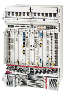 The 6500-T12 has 12 service slots which house either service interfaces or photonic modules. There are also 2 control modules. Shown at the base of the chassis are four 500 Gig switching modules. Source: Ciena
The 500 gigabit switching per slot means the 6500-12T supports 6 terabits of switching capacity while the -24T will support 12 terabits by year end. The platforms have been tested and will support 1 terabit per slot, such that the -24T will deliver the full 24 terabit. Over 100 terabit of switching capacity will be possible in a multiple-chassis configuration, managed as a single switching node.
The latest platforms can use Ciena's existing coherent line cards that support two 100 gigabit wavelengths. The T-Series also supports a 500-gigabit coherent line card with five CFP2-ACOs coupled with Ciena's WaveLogic 3 Nano DSP-ASIC.
"We will support higher-capacity wavelengths in a muxponder configuration using our existing S-series," says Xenos. "But for switching applications, switching lower-speed traffic across the shelf onto a very high-capacity wavelength, this is something that the T-series would be used for."
The T-series also adds a denser, larger-degree ROADM, from an existing 6500 S-series 8-degree to a 16-degree flexible grid, colourless, directionless and contentionless (CDC) design. Xenos says the ROADM design is also more compact such that the line amplifiers fit on the same card.
"The requirements of this platform is that it has full integration of layer 0, layer 1 and layer 2 functions," says Xenos.
The 6500 T-series supports open application programming interfaces (APIs) and is being incorporated as part of Ciena's Emulation Cloud. The Emulation Cloud enabling customers to test software on simulated network configurations without requiring 6500 hardware and is being demonstrated at OFC 2016.
The 6500 is also being integrated as part of Ciena's Blue Planet orchestration and management architecture.
OFC 2016: 20-plus technical paper highlights
To download a copy of the complete mind map, click here.
OFC 2016: a sample of the technical paper highlights
Here is a small sample of the technical paper highlights being presented at the conference.
Doubling core network capacity
Microsoft has conducted a study measuring the performance of its North American core backbone network to determine how the use of bandwidth-variable transceivers (BVTs) could boost capacity.
The highest capacity modulation scheme suited for each link from the choice of polarisation-multiplexed, quadrature phase-shift keying (PM-QPSK), polarisation-multiplexed, 8 quadrature amplitude modulation (PM-8QAM) and PM-16QAM can then be used.
By measuring the signal (Q-factor) for all its PM-QPSK based 100 gigabit links, Microsoft's study found that network capacity could be increased by 70 percent using BVTs. Equally, having the ability to increase capacity in 25-gigabit increments would increase capacity by a further 16 percent while a finer resolution of 1-gigabit would add an extra 13 percent.
Microsoft says such tuning of links need not be done in real time but rather when a link is commissioned or undergoing maintenance.
[paper M2J.2]
Architecting a new metro
How can operators redesign their metro network to enable rapid service innovation? This is the subject of a joint paper from AT&T, the Open Networking Lab and Stanford University. The work is part of a programme dubbed CORD to redesign the central office as a data centre using commodity hardware and open software to enable the rapid scaling of services. In particular, OpenFlow-enabled white boxes, the Open Network Operating System (ONOS) - a software-defined networking (SDN) operating system, and network control and management applications are used.
As part of CORD, three legacy telecom devices - optical line termination (OLT), customer premises equipment (CPE), and broadband network gateways (BNG) - have been virtualised and implemented on servers.
The paper details how a single SDN control plane based on ONOS is used to create a converged packet-optical metro network and how its support for bandwidth on-demand and automatic restoration at the optical level is used for enterprise connectivity and video distribution services.
The paper also discusses how the metro architecture supports 'disaggregated' reconfigurable optical add/ drop multiplexers (ROADMs). By disaggregating a chassis-based ROADM into commodity components, an operator can size its infrastructure as required and grow it with demand, the paper says.
[paper Th1A.7]
400 gigabit single-carrier transmission
Nokia Bell Labs reports work on 400 gigabit-per-second (Gbps) single-carrier optical transmission over submarine distances. The attraction of adopting 400 gigabit single-carrier transmission as that it is the most efficient way to reduce the cost-per-bit of optical transmission systems.
The Bell Labs' paper reviews state-of-the-art 400 gigabit single-channel transmissions over 6,000km and greater distances, and discusses the tradeoffs between such variables as symbol rate, modulation and forward error correction (FEC) schemes.
400Gbps single-carrier submarine transmission is likely in the next few years
PM-16QAM is proposed as a promising modulation scheme to achieve beyond 6,000km distances and a spectral efficiency exceeding 5b/s/Hz. But this requires a symbol rate of greater than 60 gigabaud to accommodate the 20 percent overhead FEC. Pulse-shaping at the transmitter is also used.
Exploring the receiver performance with the varying symbol rate/ FEC overhead, Bell Labs reports that the best tradeoff between coding gain and implementation penalties is 64 gigabaud and 27.3% overhead. It concludes that single-carrier 400Gbps submarine transmission is likely in the next few years.
[paper Th1B.4]
Silicon modulator for CFP2-ACOs
Cisco has developed a compact flip-chip assembly that combines a silicon photonics modulator and a silicon germanium BiCMOS Mach-Zehnder modulator driver. Such an assembly forms the basis for low-cost advanced coherent optical transceivers such as the CFP2-ACO.
Cisco has demonstrated the assembly operating at 128.7Gbps using PM-QPSK and 257.3Gbps using PM-16QAM. Cisco believes this is the first demonstration of transmission at 257.3Gbps using PM-16QAM over 1,200km of standard single-mode fibre using a silicon photonics-based device.
The modulator has also been demonstrated operating at 321.4Gbps using PM-16QAM transmission and a 20 percent FEC overhead, the highest bit rate yet achieved using a silicon-photonics based transmitter, claims Cisco.
Cisco is already using CFP2-ACO modules as part of its NCS 1002 data centre interconnect platform that implement PM-16QAM and deliver 250 gigabit due to the use of a higher baud rate than the 32 gigabaud used for existing 100-gigabit coherent systems.
[paper Th1F.2]
Flexible Ethernet to exploit line-side efficiencies
Given how the optical network network is starting to use adaptive-rate interfaces, a paper from Google asks how the client side can benefit from such line-side flexibility.
The paper points out that traditional DWDM transport equipment typically multiplexes lower-rate client ports but that this doesn't apply to network operators that manage their own data centres. Here, traffic is exclusively packet-based from IP routers and typically matches the line rate. This is why data centre interconnect platforms have become popular as they require limited grooming capability.
Google highlights how Flexible Ethernet (FlexE), for which the Optical Internetworking Forum has just defined an Implementation Agreement for, combined with data centre interconnect equipment is an extremely effective combination.
FlexE supports Ethernet MAC rates independent of the Ethernet physical layer rate being used. Google shows examples of how using FlexE, sub client rates can match the line-side rate as well as how multiple client ports can support a higher speed router logical port.
The paper concludes that combining FlexE with data centre interconnect results in a low cost, low power, compact design that will enable Internet content providers to scale their networks.
[paper W4G.4]