
Interview: Finisar’s CEO reflects on a notable year
Michael Hurlston has had an eventful 2018.
The year started with him replacing Finisar’s veteran CEO, Jerry Rawls, and it is now ending with Finisar being acquired by the firm II-VI for $3.2 billion.
Finisar is Hurlston’s first experience in the optical component industry, having spent his career in semiconductors. One year in and he already has strong views about the industry and its direction.

Michael Hurlston
“We have seen in the semiconductor industry a period of massive consolidation in the last three to four years,” says Hurlston, in his first interview sinced the deal was announced. “I think it is not that different in optics: scales matters.”
Hurlston says that, right from the start, he recognised the need to drive industry consolidation. “We had started thinking about that fairly deeply at the time the Lumentum-Oclaro acquisition was announced and that gave us more impetus to look at this,” says Hurlston. The result was revealed in November with the announced acquisition of Finisar by II-VI.
“Finisar considered so many deals in the past but could not converge on a solution,” says Vladimir Kozlov, CEO and founder of market research firm, LightCounting. "It needed a new CEO to bring a different perspective. The new II-VI will look more like many diversified semiconductor vendors, addressing multiple markets: automotive, industrial and communications."
“We really have two complementary companies for the most part,” says Hurlston, who highlights VCSELs and reconfigurable optical add-drop multiplexers (ROADMs) as the only product segments where there is overlap. Merging II-VI and Finisar with disparate portfolios further benefits scale, he says.
Chip background
Hurlston’s semiconductor experience was gained at Broadcom and involved Wi-Fi devices. The key lessons he learned there is the importance of offering differentiated products to customers and the need to expand into new application areas.
“Wi-Fi is a standard, a technology, that has rules as you have to interoperate between different chipsets and different producers,” says Hurlston. “But we did find ways to differentiate under a standards umbrella.”
>
“It turns out co-packaging is a great top-line opportunity for optics companies because eventually we will be tasked with pulling together that sub-system”
What he has found, to his surprise, is that it is harder to differentiate in the optical components industry. “What we are trying to do is find spots where we can offer differentiation,” says Hurlston.
Optical components usage needs to also expand into new segments, he says, just as Wi-Fi evolved from a PC-centric technology to home networking and ultimately mobile handsets.
Hurlston cites as an example in the optical components industry how VCSELs are now being used for 3D sensing in handsets. There are also emerging opportunities in automotive and the data centre.
For the automative market, applications include in-cabin sensing to assist drivers and LIDAR (laser detection and ranging) to help vehicles build up an image of their surroundings in real-time. “LIDAR is further out but it is a significant opportunity,” says Hurlston.
For data centres, a key opportunity silicon co-packaging: bringing optics closer to switch silicon.
Currently, switch platform use pluggable optical modules on the faceplate to send and receive data. But with switch silicon capacity doubling every two years, the speed and density of the input-output means optics will have to get closer to the switch silicon.
On-board optics - as promoted by the Consortium for On-Board Optics (COBO) - is one option. Another is co-packaged optics, where the optics and silicon are placed in the same package.
“It turns out co-packaging is a great top-line opportunity for optics companies because eventually we will be tasked with pulling together that sub-system,” says Hurlston. “The integration of the switch chip and optics is something that will be technically difficult and necessitate differentiation.”
Challenges
As well as the issue of acquisitions, another area Hurlston has tackled in his short tenure is Finisar’s manufacturing model and how it can be improved.
“Finisar is a technology company at heart but the life-blood of the company is manufacturing,” he says.
Manufacturing is also one area where there is a notable difference between chips and optics. “There are manufacturing complexities with semiconductors and semiconductor process but optics takes it to a whole different level,” he says.
This is due to the manufacturing complexity of optical transceiver which Finisar’s CEO likens to manufacturing a mobile phone. There are chips that need a printed circuit board onto which are also added optical subassemblies housing such components as lasers and photo-detectors.
“Part of it [the complexity] is the human labour - the human touch - that is involved in the manufacturing and assembling of these transceivers ” he says. Finisar says its laser fab employs several hundred people whereas its optical transceiver factories employ thousands: 5,000 staff in Malaysia and some 5,500 in China.
“Our manufacturing model has been where I’ve spent a lot of time,” says Hurston. Some efficiencies have been gained but not nearly as much as he initially hoped.
Consolidation
One of the issues that has hindered greater industry consolidation has been the need for synergy between companies. A semiconductor company will only acquire or merge with another semiconductor company, and the same with a laser company looking for another laser player, he says. “What I admire about II-VI is that they are pretty bold,” says Hurlston. “What II-VI did is go after something that is not overlapping.”
He believes the creation of such broad-based suppliers is something the optics industry will have to do more of: “The transceiver guys are going to have to go after different areas of the value chain.”
In most mature industries, three large diversified companies typically dominate the marketplace. Given Lumentum’s acquisition of Oclaro has just closed and II-VI’s acquisition of Finisar is due to be completed in mid-2019, will there be another large deal?
“This is a big industry and the opportunity today and going forward is big,” says Hurlston. But there are so many players in different parts of the supply chain such that he is unsure whether these niche companies will survive in the long run.
“Whether there will be three, four or five large players, I don’t know,” he says. “But we are definitely going to see fewer; this [II-VI - Finisar deal] isn't the last transaction that drives industry consolidation.”
>
“Whether there will be three, four or five large players, I don’t know but we are definitely going to see fewer”
How will Finisar make optical transceivers in such a competitive marketplace, that includes an increasing number of Chinese entrants, while delivering gross margins that meet Wall Street expectations?
Finisar does have certain advantages, he says, such as making its own lasers. “We also make our own semiconductors, a lot of the semiconductor solutions the Chinese guys have are sourced,” he says. “That gives us an inherent advantage.”
Having its own manufacturing facilities in the Far East means that Chinese players have no inherent manufacturing advantage there. However, he admits that the gross margin expected of Finisar is higher that its Chinese competitors.
This is why Finisar’s CEO stresses the need to pursue pockets of differentiation and why the company has to be first to market in important productareas that all players will target. “We historically have not been first to market,” he says. “We have made adjustments in the last year in our time-to-market and our ability to get to big products transitions that will be hyper-competitive first.”
Hurston expresses some satisfaction in the improved revenues and gross margins as reported in Finisar’s last two quarters’ results, albeit these quarters coming after what he calls ‘a low base’.
“We have also made significant progress in 3D sensing that has been a big challenge for us,” he says.
What next?
Hurlston says he hopes to have a role in the new company once the deal closes.
“But If I don’t, I’ve really enjoyed working with the [Finisar] team and in this space,” he says. “It’s been a bit of a learning curve but I’ve learnt a couple of tricks. Hopefully there will be another opportunity to apply some of that learning to a job elsewhere.”
Finisar's 10 Gig bi-directional DWDM architecture
Finisar has developed a bi-directional 10-gigabit SFP+ module for the metro-access market. The dense wavelength-division multiplexing (DWDM) module is designed to expand capacity at locations where fibre is scarce. And being tunable, the SFP+ also simplifies network planning for the operators.
Finisar demonstrated the module working at the recent ECOC 2017 show held in Gothenburg.
Market applications
Interest is growing in using WDM optics for wireless, metro-access and cable networks that are undergoing upgrades. The interest in WDM at the network edge is due to a need to use fibre resources more efficiently. “We are seeing that globally, more and more dark fibre is being used up,” says Leo Lin, director of product line management at Finisar.
 Leo LinGiven the cost of leasing and installing fibre, operators are keen to make the best use of their existing fibre and are willing to pay more for WDM optics.
According to Finisar, leasing a fibre can cost $250-$2,000 per fibre annually while the cost of installing fibre can be $500,000 per 10km. “Using WDM optics, you can get payback in less than a year,” says Lin.
LightCounting Market Research's latest forecast estimates that the global wireless transceiver market for 10 gigabit WDM will be approximately $400 million in 2022.
Finisar’s bi-directional 10-gigabit SFP+ product is also being aimed at two emerging ITU Telecom standards: G.metro and NG-PON2.
G.Metro and NG-PON2
The G.metro standard supports up to 40 DWDM wavelengths on a 100GHz wavelength grid. Tuneable transponders each at 10 gigabits-per-second (Gbps) are used and have a reach of up to 20km without amplification.
NG-PON2 is a time and wavelength division multiplexing, passive optical network (TWDM-PON) standard. “In addition to TWDM-PON, they want to have a few dedicated point-to-point WDM links, an overlay on top of the PON,” says Lin.
G.metro uses both the C-band and the L-band: one band is used for the sent wavelengths and the other band for the received wavelengths. In contrast, Finisar’s bi-directional approach sends and receives wavelengths using the C-band only.
“The G.metro standard calls out bi-directional and tuneable optics, and our bi-directional module product can be directly used here,” says Lin. “Since ECOC, we have had quite some support from operators and OEMs that will add our architecture as one of the channel options in both G.metro and NG-PON2.”
Bidi design
Finisar describes its design as a dual-band bi-directional DWDM approach. To understand the design, it helps to compare it to existing DWDM duplex and single fibre schemes.
 Standard DWDM (A), a hybrid bi-directional scheme that uses 50GHz AWGs (B), and the bi-directional approach (C) using the C- and L-bands being proposed for G.metro and NG-PON2. Finisar's approach is shown in the diagram below. Source Finisar.
With standard DWDM, two fibres are used, each having a multiplexer and demultiplexer pair. The C-band is used with wavelengths sent down one fibre and received on the other (see diagram A).
The hybrid bi-directional DWDM design (diagram B) sends wavelengths in both directions on one fibre. The hybrid approach is growing in popularity, says Finisar, to address fibre scarcity, for example between a central office and a remote node. For the hybrid scheme, only a single multiplexer-demultiplexer pair is needed. But to fit all the wavelengths on one fibre, a 50GHz channel mux-demux is used rather than a cheaper 100GHz one.
Another bi-directional scheme - one that G.metro and NG-PON2 are promoting - uses 100GHz channels but requires both the C-band and the L-band (diagram C). Here, east-to-west traffic is sent across one band while west-to-east traffic is sent on the other.
“This approach requires cyclic arrayed-waveguide gratings,” says Lin. A cyclic or colourless arrayed-waveguide grating (AWG) can separate or combine wavelengths across multiple bands. But unlike the hybrid bi-directional case, one fibre only connects to each bi-directional transceiver hosting a C-band wavelength in one direction and an L-band one travelling in the opposite direction. Using fewer fibres saves cost and space.
Finisar’s bi-directional design is similar but with one important twist: only the C-band is used.
To do this, two carriers are placed into the single 100GHz channel: one an upstream wavelength and one a downstream one. The result is 40, 10Gbps wavelengths - 80 carriers in total - spread across the C-band (see diagram below).
 Finisar's bi-directional architecture uses two carriers per channel spread across the C-band. Source: Finisar
A tuneable filter is used in the module not only to match the channel that the remote module’s tuneable laser will use, but also to select the particular band in a given channel, either the upstream or downstream band. The result is that one bi-directional module can be used for all 40 channels. “One single part number for the far end and the near end,” says Lin.
The technical challenge Finisar faced to make its design work is separating the two closely spaced carriers in a 100GHz channel.
Finisar says that with a 50GHz DWDM system, the wavelength must sit centrally in the channel and that requires a wavelength locker. The two carriers within its 100GHz band are not placed centrally yet Finisar has developed a way to separate the two without needing wavelength-locker technology.
The tuneable bi-directional approach also simplifies network planning. If an operator wants to add a new wavelength and drop it at an existing node, the node’s optical add-drop multiplexer does not need to be upgraded.
“All operators have different channel plans and customised optical add-drop multiplexers in the field,” says Lin. “In our case, we are even simpler than the duplex. In duplex you need a multiplexer-demultiplexer pair; in our case, any AWG or thin-film filter based design can be used.”
Finisar uses an out-of-band communication channel for the central office module to co-ordinate the channel to be used with a newly inserted remote module. “You can plug in a module on any available port and it establishes a link by itself in under 10 seconds,” says Lin.
Roadmap
Finisar is working to extend the reach of its 10-gigabit bi-directional tuneable SFP+ DWDM architecture to beyond the current 40km to 60km with the use of a bi-directional EDFA.
The current 40km reach is determined by the link budget chosen for the expected use cases with the assumption being that multiple add-drop sites will exist between the central office and the remote end. “The tuneable laser used is the same that is used in our tuneable XFP+, so supporting beyond 80km is not a problem,” says Lin.
Finisar says it is working on a 25-gigabit bi-directional module that will be available in 2019.
Meanwhile, select customers are evaluating samples of the 10-gigabit bi-directional SFP+ module. General availability is expected by mid-2018.
Oclaro’s 400-gigabit plans
Adam Carter, Oclaro’s chief commercial officer, discusses the company’s 400-gigabit and higher-speed coherent optical transmission plans and the 400-gigabit client-side pluggable opportunity.
Oclaro showcased its first coherent module that uses Ciena’s WaveLogic Ai digital signal processor at the ECOC show held recently in Gothenburg.
 Adam CarterOclaro is one of three optical module makers, the others being Lumentum and NeoPhotonics, that signed an agreement with Ciena earlier this year to use the system vendor’s DSP technology and know-how to bring coherent modules to market. The first product resulting from the collaboration is a 5x7-inch board-mounted module that supports 400-gigabits on a single-wavelength.
The first WaveLogic Ai-based modules are already being tested at several of Oclaro’s customers’ labs. “They [the module samples] are very preliminary,” says Adam Carter, the chief commercial officer at Oclaro. “The really important timeframe is when we get towards the new year because then we will have beta samples.”
DSP developments
The coherent module is a Ciena design and Carter admits there isn’t going to be much differentiation between the three module makers’ products.
“We have some of the key components that sit inside that module and the idea is, over time, we would design in the rest of the componentry that we make that isn’t already in there,” says Carter. “But it is still going to be the same spec between the three suppliers.”
The collaboration with the module makers helps Ciena promote its coherent DSP to a wider market and in particular China, a market where its systems are not deployed.
Over time, the scope for differentiation between the three module makers will grow. “It [the deal] gives us access to another DSP chip for potential future applications,” says Carter.
Here, Oclaro will be the design authority, procuring the DSP chip for Ciena before adding its own optics. “So, for example, for the [OIF’s] 400G ZR, we would ask Ciena to develop a chip to a certain spec and then put our optical sub-assemblies around it,” says Carter. “This is where we do believe we can differentiate.”
Oclaro also unveiled at ECOC an integrated coherent transmitter and an intradyne coherent receiver optical sub-assemblies using its indium phosphide technology that operate at up to 64 gigabaud (Gbaud).
We expect to see 64Gbaud optical systems being trialed in 2018 with production systems following at the end of next year
A 64Gbaud symbol rate enables a 400-gigabit wavelength using 16-ary quadrature amplitude modulation (16-QAM) and a 600-gigabit wavelength using 64-QAM.
Certain customers want such optical sub-assemblies for their line card designs and Oclaro will also use the building blocks for its own modules. The devices will be available this quarter. “We expect to see 64Gbaud optical systems being trialed in 2018 with production systems following at the end of next year and the beginning of 2019,” says Carter.
Oclaro also announced that its lithium niobate modulator supporting 400-gigabit single wavelengths is now in volume production. “Certain customers do have their preferences when it comes to first designs and particularly for long-reach systems,” says Carter. “Lithium niobate seems to be the one people go with.”
400-gigabit form factors
Oclaro did not make any announcements regarding 400-gigabit client-side modules at ECOC. At the OFC show held earlier this year, it detailed two CFP8-based 400-gigabit designs based on eight wavelengths with reaches of 10km and 40km.
“We are sampling the 400-gigabit 10km product right now,” says Carter. “The product is being tested at the system level and will go through various qualification runs.”
The 40km CFP8 product is further out. There are customers interested in such a module as they have requirements to link IP routers that are more than 10km apart.
Carter describes the CFP8 400-gigabit modules as first-generation products. The CFP8 is similar in size to the CFP2 pluggable module and that is too large for the large-scale data centre players. They want higher aggregate bandwidth and greater front panel densities for their switches and are looking such form factors as the double-density QSFP (QSFP-DD) and the Octal Small Form Factor pluggable (OSFP).
The OSFP is a fresh design, has a larger power envelope - some 15W compared to the 12W of the QSFP-DD - and has a roadmap that supports 800-gigabit data rates. In contrast, the QSFP-DD is backward compatible with the QSFP, an attractive feature for many vendors.
But it is not only a module’s power envelope that is an issue for 400-gigabit designs but also whether a one-rack-unit box can be sufficiently cooled when fully populated to avoid thermal runaway. Some 36 QSFP-DDs can fit on the front panel compared to 32 OSFPs.
Carter stresses both form factors can’t be dismissed for 400-gigabit: “Everyone is pursuing designs that are suitable for both.” Oclaro is not an advocate of either form factor given it provides optical sub-assemblies suitable for both.
The industry really wants four-channels. When you use more lasers, you are adding more cost.
Optical formats
Oclaro’s core technology is indium phosphide and, as such, its focusses on single-mode fibre designs.
The single mode options for 400 gigabits are split between eight-wavelength designs such as the IEEE 802.3bs 2km 400GBASE-FR8 and 10km 400GBASE-LR8 and the newly announced CWDM8 MSA, and four-wavelength specifications - the 500m IEEE 802.3bs parallel fibre 400GBASE-DR4 and the 2km 100G Lambda MSA 400G-FR4 that is under development. Oclaro is a founding member of the 100 Gigabit Lambda MSA but has not joined the CWDM8 MSA.
"The industry really wants four channels," says Carter. "When you use more lasers, you are adding more cost." It is also not trivial fitting eight lasers into a CFP8 never mind into the smaller QSFP-DD and OSFP modules.
“There might be some that have the technology to do the eight-channel part and there might be customers that will use that,” says Carter. “But most of the discussions we’ve been having are around four channels.”
Challenges
The industry’s goal is to have 400-gigabit QSFP-DD and OSFP module in production by the end of next year and into 2019. “There is still some risk but everybody is driving to meet that schedule,” says Carter.
Oclaro says first samples of 100-gigabit PAM-4 chips needed for 100-gigabit single wavelengths are now in the labs. Module makers can thus add their optical sub-assemblies to the chips and start testing system performance. Four-channel PAM-4 chips will be needed for the 400-gigabit module products.
Carter also acknowledges that any further delay in four-wavelength designs could open the door for other 400-gigabit solutions and even interim 200-gigabit designs.
“As a transceiver supplier and an optical component supplier you are always aware of that,” he says. “You have to have backup plans if that comes off.”
The era of cloud-scale routeing
 Nokia's FP4 p-chip. The multi-chip module shows five packages: the p-chip die surrounded by four memory stacks. Each stack has five memory die. The p-chip and memory stacks are interconnected using an interposer.
 - Nokia has unveiled the FP4, a 2.4 terabit-per-second network processor that has 6x the throughput of its existing FP3.
- The FP4 is a four-IC chipset implemented using 16nm CMOS FinFET technology. Two of the four devices in the chipset are multi-chip modules.
- The FP4 uses 56 gigabit-per-second serial-deserialiser (serdes) technology from Broadcom, implemented using PAM-4 modulation. It also supports terabit flows.
- Nokia announced IP edge and core router platforms that will use the FP4, the largest configuration being a 0.58 petabit switching capacity router.
Much can happen in an internet minute. In that time, 4.1 million YouTube videos are viewed, compared to 2.8 million views a minute only last year. Meanwhile, new internet uses continue to emerge. Take voice-activated devices, for example. Amazon ships 50 of its Echo devices every minute, almost one a second.
Given all that happens each minute, predicting where the internet will be in a decade’s time is challenging. But that is the task Alcatel-Lucent’s (now Nokia’s) chip designers set themselves in 2011 after the launch of its FP3 network processor chipset that powers its IP-router platforms.
Six years on and its successor - the FP4 - has just been announced. The FP4 is the industry’s first multi-terabit network processor that will be the mainstay of Nokia’s IP router platforms for years to come.
Cloud-scale routing
At the FP4’s launch, Nokia’s CEO, Rajeev Suri, discussed the ‘next chapter’ of the internet that includes smart cities, new higher-definition video formats and the growing number of connected devices.
IP traffic is growing at a compound annual growth rate (CAGR) of 25 percent through to 2022, according to Nokia Bell Labs, while peak data rates are growing at a 39 percent CAGR. Nokia Bell Labs also forecasts that the number of connected devices will grow from 12 billion this year to 100 billion by 2025.
Basil Alwan, Nokia’s president of IP and optical networks, said the internet has entered the era of cloud-scale routeing. When delivering a cloud service, rarely is the request fulfilled by one data centre. Rather, several data centres are involved in fulfilling the tasks. “One transaction to the cloud is multiplied,” said Alwan.
IP traffic is also becoming more dynamic, while the Internet of Things presents a massive security challenge.
Alwan also mentioned how internet content providers have much greater visibility into their traffic whereas the telcos’ view of what flows in their networks is limited. Hence their interest in analytics to understand and manage their networks better.
These are the trends that influenced the design of the FP4.
We put a big emphasis on making sure we had a high degree of telemetry coming out at the chip level
FP4 goals
Telemetry, the sending of measurement data for monitoring purposes, and network security were two key design goals for the FP4.
 Steve Vogelsang“We put a big emphasis on making sure we had a high degree of telemetry coming out at the chip level,” said Steve Vogelsang, CTO for Nokia's IP and optical business.
Tasks include counters, collecting statistics and packet copying. “This is to make sure we have the instrumentation coming off these systems that we can use to drive the [network] analytics platform,” said Vogelsang.
Being able to see the applications flowing in the network benefits security. Distributed Denial-of-Service (DDoS) attacks are handled by diverting traffic to a ‘scrubbing centre’ where sophisticated equipment separates legitimate IP packets from attack traffic that needs scrubbing.
The FP4 supports the deeper inspection of packets. “Once we identify a threat, we can scrub that traffic directly in the network,” said Vogelsang. Nokia claims that that the FP4 can deal with over 90 percent of the traffic that would normally go to a scrubbing centre.
Chipset architecture
Nokia’s current FP3 network processor chipset comprises three devices: the p-chip network processor, the q-chip traffic manager and the t-chip fabric interface device.
The p-chip network processor inspects packets and performs table look-ups using fast-access memory to determine where packets should be forwarded. The q-chip is the traffic manager that oversees the packet flows and decides how packets should be dealt with, especially when congestion occurs. The third FP3 chip is the t-chip that interfaces to the router fabric.
The FP4 retains the three chips and adds a fourth: the e-chip - a media access controller (MAC) that parcels data from the router’s client-side pluggable optical modules for the p-chip. However, while the FP4 retains the same nomenclature for the chips as the FP3, the CMOS process, chip architecture and packaging used to implement the FP4 are significantly more advanced.
The FP4 can deal with over 90 percent of the traffic that would normally go to a scrubbing centre
Nokia is not providing much detail regarding FP4 chipset's architecture, unlike the launch of the FP3. “We wanted to focus on the re-architecture we have gone through,” said Vogelsang. But looking at the FP3 design, insight can be gained as to how the FP4 has likely changed.
The FP3’s p-chip uses 288 programmable cores. Each programmable core can process two instructions each clock cycle and is clocked at 1GHz.
The 288 cores are arranged as a 32-row-by-9-column array. Each row of cores can be viewed as a packet-processing pipeline. A row pipeline can also be segmented to perform independent tasks. The array’s columns are associated with table look-ups. The resulting FP3 p-chip is a 400-gigabit network processor.
Vogelsang said there is limited scope to increase the clock speed of the FP4 p-chip beyond 1GHz. Accordingly, the bulk of the FP4’s sixfold throughput improvement is the result of a combination of programmable core enhancements, possible a larger core array and, most importantly, system improvements. In particular, the memory architecture is now packaged within the p-chip for fast look-ups, while the chipset’s input-output lanes have been boosted from 10 gigabits-per-second (Gbps) to 50Gbps.
Nokia has sought to reuse as much of the existing microcode to program the cores for the FP4 p-chip but has added new instructions to take advantage of changes in the pipeline.
Software compatibility already exists at the router operating system level. The same SROS router operating system runs on Nokia’s network processors, merchant hardware from the like of Broadcom and on x86 instruction-set microprocessors in servers using virtualisation technology.
Such compatibility is achieved using a hardware abstraction layer that sits between the operating system and the underlying hardware. “The majority of the software we write has no idea what the underlying hardware is,” said Vogelsang.
Nokia has a small team of software engineers focussed on the FP4’s microcode changes but, due to the hardware abstraction layer, such changes are transparent to the main software developers.
The FP3’s traffic manager, the q-chip, comprises four reduced instruction set computer (RISC) cores clocked at 900MHz. This too has been scaled up for the FP4 but Nokia has not given details.
The t-chip interfaces to the switch fabric that sits on a separate card. In previous generations of router products, a mid-plane is used, said Nokia. This has been scrapped with the new router products being announced. Instead, the switch cards are held horizontally in the chassis and the line cards are vertical. “A bunch of metal guides are used to guide the two cards and they directly connect to each other,” said Vogelsang. “The t-chips are what interface to these connectors inside the system.”
The MAC e-chip interfaces to the line card’s pluggable modules and support up to a terabit flow. Indeed, the MAC will support integer multiples of 100 Gigabit Ethernet from 100 gigabit to 1 terabit. Nokia has a pre-standard implementation of FlexMAC that allows it to combine lanes across multiple transceivers into a single interface.
Nokia will have line cards that support 24 or 36 QSFP-DD pluggable modules, with each module able to support 400 Gigabit Ethernet.
The FP4 is also twice as power efficient, consuming 4 gigabit/W.
We wanted to make sure we used a high-volume chip-packaging technology that was being driven by other industries and we found that in the gaming industry
Design choices
One significance difference between the two network processor generations is the CMOS process used. Nokia skipped 28nm and 22nm CMOS nodes to go from 40nm CMOS for the FP3 to 16nm FinFET for the FP4. “We looked at that and we did not see all the technologies we would need coming together to get the step-function in performance that we wanted,” said Vogelsang.
Nokia also designed its own memory for the FP4.
“A challenge we face with each generation of network processor is finding memories and memory suppliers that can offer the performance we need,” said Vogelsang. The memory Nokia designed is described as intelligent: instructions can effectively be implemented during memory access and the memory can be allocated to do different types of look-up and buffering, depending on requirements.
Another key area associated with maximising the performance of the memory is the packaging. Nokia has adopted multi-chip module technology for the p-chip and the q-chip.
“We wanted to make sure we used a high-volume chip-packaging technology that was being driven by other industries and we found that in the gaming industry,” said Vogelsang, pointing out that the graphics processing unit (GPU) has similar requirements to those of a network processor. GPUs are highly memory intensive while manipulating bits on a screen is similar to manipulating headers and packets.
The resulting 2.5D packaged p-chip comprises the packet processor die and stacks of memory. Each memory stack comprises 5 memory die. All sit on an interposer substrate - itself a die that is used for dense interconnect of devices. The resulting FP4 p-chip is thus a 22-die multi-chip module.
“Our memory stacks are connected at the die edges and do not use through-silicon vias,” said Vogelsang. “Hence it is technically a 2.5D package [rather than 3D].”
The q-chip is also implemented as a multi-chip module containing RISC processors and buffering memory, whereas the router fabric t-chip and MAC e-chip are single-die ICs.
The FP4’s more advanced CMOS process also enables significantly faster interfaces. The FP4 uses PAM-4 modulation to implement 56Gbps interfaces. “You really need to run those bit rates much much higher to get the traffic into and out of the chip,” said Vogelsang.
Nokia says it is using embedded serialiser-deserialiser interface technology from Broadcom.
Next-gen routers
Nokia has also detailed the IP edge and core routers that will use the FP4 network processor.
The 7750 Service Router (SR-s) edge router family will support up to 144 terabits in a single shelf. This highest capacity configuration is the 7750 SR-14. It is a 24-rack-unit-plus-the-power-supply high chassis and supports a dozen line cards, each 12Tbps when using 100-gigabit modules, or 24x400GbE when using QSFP-DD modules.
Another new platform is the huge 7950 Extensible Routing System (XRS-XC) IP core router which can be scaled to 576 terabits - over half a petabit - when used in a six-chassis configuration. Combining the six chassis does not make require the use of front-panel client-side interfaces. Instead, dedicated interfaces are used with active optical cables to interlink the chassis.
The first router products will be shipped to customers at the year end with general availability expected from the first quarter of 2018.
Meeting the many needs of data centre interconnect
High capacity. Density. Power efficiency. Client-side optical interface choices. Coherent transmission. Direct detection. Open line system. Just some of the requirements vendors must offer to compete in the data centre interconnect market.
“A key lesson learned from all our interactions over the years is that there is no one-size-fits-all solution,” says Jörg-Peter Elbers, senior vice president of advanced technology, standards and IPR at ADVA Optical Networking. “What is important is that you have a portfolio to give customers what they need.”
 Jörg-Peter Elbers
Teraflex
ADVA Optical Networking detailed its Teraflex, the latest addition to its CloudConnect family of data centre interconnect products, at the OFC show held in Los Angeles in March (see video).
The platform is designed to meet the demanding needs of the large-scale data centre operators that want high-capacity, compact platforms that are also power efficient.
A key lesson learned from all our interactions over the years is that there is no one-size-fits-all solution
Teraflex is a one-rack-unit (1RU) stackable chassis that supports three hot-pluggable 1.2-terabit modules or ‘sleds’. A sled supports two line-side wavelengths, each capable of coherent transmission at up to 600 gigabits-per-second (Gbps). Each sled’s front panel supports various client-side interface module options: 12 x 100-gigabit QSFPs, 3 x 400-gigabit QSFP-DDs and lower speed 10-gigabit and 40-gigabit modules using ADVA Optical Networking’s MicroMux technology.
“Building a product optimised only for 400-gigabit would not hit the market with the right feature set,” says Elbers. “We need to give customers the possibility to address all the different scenarios in one competitive platform.”
The Teraflex achieves 600Gbps wavelengths using a 64-gigabaud symbol rate and 64-ary quadrature-amplitude modulation (64-QAM). ADVA Optical Networking is using Acacia’s Communications latest Pico dual-core coherent digital signal processor (DSP) to implement the 600-gigabit wavelengths. ADVA Optical Networking would not confirm Acacia is its supplier but Acacia decided to detail the Pico DSP at OFC because it wanted to end speculation as to the source of the coherent DSP for the Teraflex. That said, ADVA Optical Networking points out that Teraflex’s modular nature means coherent DSPs from various suppliers can be used.
 The 1 rack unit Teraflex
The line-side optics supports a variety of line speeds – from 600Gbps to 100Gbps, the lower the speed, the longer the reach.
The resulting 3-sled 1RU Teraflex platform thus supports up to 3.6 terabits-per-second (Tbps) of duplex communications. This compares to a maximum 800Gbps per rack unit using the current densest CloudConnect 0.5RU Quadflex card.
Markets
The data centre interconnect market is commonly split into metro and long haul.
The metro data centre interconnect market requires high-capacity, short-haul, point-to-point links up to 80km. Large-scale data centre operators may have several sites spread across a city, given they must pick locations where they can find them. Sites are typically no further apart than 80km to ensure a low-enough latency such that, collectively, they appear as one large logical data centre.
“You are extending the fabric inside the data centre across the data-centre boundary, which means the whole bandwidth you have on the fabric needs to be fed across the fibre link,” says Elbers. “If not, then there are bottlenecks and you are restricted in the flexibility you have.”
Large enterprises also use metro data centre interconnect. The enterprises’ businesses involve processing customer data - airline bookings, for example - and they cannot afford disruption. As a result, they may use twin data centres to ensure business continuity.
Here, too, latency is an issue especially if synchronous mirroring of data using Fibre Channel takes place between sites. The storage protocol requires acknowledgement between the end points such that the round-trip time over the fibre is critical. “The average distance of these connections is 40km, and no one wants to go beyond 80 or 100km,” says Elbers, who stresses that this is not an application for Teraflex given it is aimed at massive Ethernet transport. Customers using Fibre Channel typically need lower capacities and use more tailored solutions for the application.
The second data centre interconnect market - long haul - has different requirements. The links are long distance and the data sent between sites is limited to what is needed. Data centres are distributed to ensure continual business operation and for quality-of-experience by delivering services closer to customers.
Hundreds of gigabits and even terabits are sent over the long-distance links between data centres sites but commonly it is about a tenth of the data sent for metro data centre interconnect, says Elbers.
Direct Detection
Given the variety of customer requirements, ADVA Optical Networking is pursuing direct-detection line-side interfaces as well as coherent-based transmission.
At OFC, the system vendor detailed work with two proponents of line-side direct-detection technology - Inphi and Ranovus - as well as its coherent-based Teraflex announcement.
Working with Microsoft, Arista and Inphi, ADVA detailed a metro data centre interconnect demonstration that involved sending 4Tbps of data over an 80km link. The link comprised 40 Inphi ColorZ QSFP modules. A ColorZ module uses two wavelengths, each carrying 56Gbps using PAM-4 signalling. This is where having an open line system is important.
Microsoft wanted to use QSFPs directly in their switches rather than deploy additional transponders, says Elbers. But this still requires line amplification while the data centre operators want the same straightforward provisioning they expect with coherent technology. To this aim, ADVA demonstrated its SmartAmp technology that not only sets up the power levels of the wavelengths and provides optical amplification but also automatically measures and compensates for chromatic dispersion experienced over a link.
ADVA also detailed a 400Gbps metro transponder card based on PAM-4 implemented using two 200Gbps transmitter optical subassemblies (TOSAs) and two 200Gbps receiver optical subassemblies (ROSAs) from Ranovus.
Clearly there is also space for a direct-detection solution but that space will narrow down over time
Choices
The decision to use coherent or direct detection line-side optics boils down to a link’s requirements and the cost an end user is willing to pay, says Elbers.
As coherent-based optics has matured, it has migrated from long-haul to metro and now data centre interconnect. One way to cost-reduce coherent further is to cram more bits per transmission. “Teraflex is adding chunks of 1.2Tbps per sled which is great for people with very high capacities,” says Elbers, but small enterprises, for example, may only need a 100-gigabit link.
“For scenarios where you don’t need to have the highest spectral efficiency and the highest fibre capacity, you can get more cost-effective solutions,” says Elbers, explaining the system vendor’s interest in direct detection.
“We are seeing coherent penetrating more and more markets but still cost and power consumption are issues,” says Elbers. “Clearly there is also space for a direct-detection solution but that space will narrow down over time.”
Developments in silicon photonics that promise to reduce the cost of optics through greater integration and the adoption of packaging techniques from the CMOS industry will all help. “We are not there yet; this will require a couple of technology iterations,” says Elbers.
Until then, ADVA’s goal is for direct detection to cost half that of coherent.
“We want to have two technologies for the different areas; there needs to be a business justification [for using direct detection],” he says. “Having differentiated pricing between the two - coherent and direct detection - is clearly one element here.”
Talking markets: Oclaro on 100 gigabits and beyond
Oclaro’s chief commercial officer, Adam Carter, discusses the 100-gigabit market, optical module trends, silicon photonics, and why this is a good time to be an optical component maker.
Oclaro has started its first quarter 2017 fiscal results as it ended fiscal year 2016 with another record quarter. The company reported revenues of $136 million in the quarter ending in September, 8 percent sequential growth and the company's fifth consecutive quarter of 7 percent or greater revenue growth.
 Adam CarterA large part of Oclaro’s growth was due to strong demand for 100 gigabits across the company’s optical module and component portfolio.
The company has been supplying 100-gigabit client-side optics using the CFP, CFP2 and CFP4 pluggable form factors for a while. “What we saw in June was the first real production ramp of our CFP2-ACO [coherent] module,” says Adam Carter, chief commercial officer at Oclaro. “We have transferred all that manufacturing over to Asia now.”
The CFP2-ACO is being used predominantly for data centre interconnect applications. But Oclaro has also seen first orders from system vendors that are supplying US communications service provider Verizon for its metro buildout.
The company is also seeing strong demand for components from China. “The China market for 100 gigabits has really grown in the last year and we expect it to be pretty stable going forward,” says Carter. LightCounting Market Research in its latest optical market forecast report highlights the importance of China’s 100-gigabit market. China’s massive deployments of FTTx and wireless front haul optics fuelled growth in 2011 to 2015, says LightCounting, but this year it is demand for 100-gigabit dense wavelength-division multiplexing and 100 Gigabit Ethernet optics that is increasing China’s share of the global market.
The China market for 100 gigabits has really grown in the last year and we expect it to be pretty stable going forward
QSFP28 modules
Oclaro is also providing 100-gigabit QSFP28 pluggables for the data centre, in particular, the 100-gigabit PSM4 parallel single-mode module and the 100-gigabit CWDM4 based on wavelength-division multiplexing technology.
2016 was expected to be the year these 100-gigabit optical modules for the data centre would take off. “It has not contributed a huge amount to date but it will start kicking in now,” says Carter. “We always signalled that it would pick up around June.”
One reason why it has taken time for the market for the 100-gigabit QSFP28 modules to take off is the investment needed to ramp manufacturing capacity to meet the demand. “The sheer volume of these modules that will be needed for one of these new big data centres is vast,” says Carter. “Everyone uses similar [manufacturing] equipment and goes to the same suppliers, so bringing in extra capacity has long lead times as well.”
Once a large-scale data centre is fully equipped and powered, it generates instant profit for an Internet content provider. “This is very rapid adoption; the instant monetisation of capital expenditure,” says Carter. “This is a very different scenario from where we were five to ten years ago with the telecom service providers."
Data centre servers and their increasing interface speed to leaf switches are what will drive module rates beyond 100 gigabits, says Carter. Ten Gigabit Ethernet links will be followed by 25 and 50 Gigabit Ethernet. “The lifecycle you have seen at the lower speeds [1 Gigabit and 10 Gigabit] is definitely being shrunk,” says Carter.
Such new speeds will spur 400-gigabit links between the data centre's leaf and spine switches, and between the spine switches. “Two hundred Gigabit Ethernet may be an intermediate step but I’m not sure if that is going to be a big volume or a niche for first movers,” says Carter.
400 gigabit CFP8
Oclaro showed a prototype 400-gigabit module in a CFP8 module at the recent ECOC show in September. The demonstrator is an 8-by-50 gigabit design using 25 gigabaud optics and PAM-4 modulation. The module implements the 400Gbase-LR8 10km standard using eight 1310nm distributed feedback lasers, each with an integrated electro-absorption modulator. The design also uses two 4-wide photo-detector arrays.
“We are using the four lasers we use for the CWDM4 100-gigabit design and we can show we have the other four [wavelength] lasers as well,” says Carter.
Carter says IP core routers will be the main application for the 400Gbase-LR8 module. The company is not yet saying when the 400-gigabit CFP8 module will be generally available.
We can definitely see the CFP2-ACO could support 400 gigabits and above
Coherent
Oclaro is already working with equipment customers to increase the line-side interface density on the front panel of their equipment.
The Optical Internetworking Forum (OIF) has already started work on the CFP8-ACO that will be able to support up to four wavelengths, each supporting up to 400 gigabits. But Carter says Oclaro is working with customers to see how the line-side capacity of the CFP2-ACO can be advanced. “We can definitely see the CFP2-ACO could support 400 gigabits and above,” says Carter. “We are working with customers as to what that looks like and what the schedule will be.”
And there are two other pluggable form factors smaller than the CFP2: the CFP4 and the QSFP28. “Will you get 400 gigabits in a QSFP28? Time will tell, although there is still more work to be done around the technology building blocks,” says Carter.
Vendors are seeking the highest aggregate front panel density, he says: “The higher aggregate bandwidth we are hearing about is 2 terabits but there is a need to potentially going to 3.2 and 4.8 terabits.”
Silicon photonics
Oclaro says it continues to watch closely silicon photonics and to question whether it is a technology that can be brought in-house. But issues remain. “This industry has always used different technologies and everything still needs light to work which means the basic III-V [compound semiconductor] lasers,” says Carter.
“Producing silicon photonics chips versus producing packaged products that meet various industry standards and specifications are still pretty challenging to do in high volume,” says Carter. And integration can be done using either silicon photonics or indium phosphide. “My feeling is that the technologies will co-exist,” says Carter.
Nokia’s PSE-2s delivers 400 gigabit on a wavelength
Four hundred gigabit transmission over a single carrier is enabled using Nokia’s second-generation programmable Photonic Service Engine coherent processor, the PSE2, part of several upgrades to Nokia's flagship PSS 1830 family of packet-optical transport platforms.
 Kyle Hollasch“One thing that is clear is that performance will have a key role to play in optics for a long time to come, including distance, capacity per fiber, and density,” says Sterling Perrin, senior analyst at Heavy Reading.
This limits the appeal of the so-called “white box” trend for many applications in optics, he says: “We will continue to see proprietary advances that boost performance in specific ways and which gain market traction with operators as a result”.
The 1830 Photonic Service Switch
The 1830 PSS family comprises dense wavelength-division multiplexing (DWDM) platforms and packet-OTN (Optical Transport Network) switches.
The DWDM platform includes line amplifiers, reconfigurable optical add-drop multiplexers (ROADMs), transponder and muxponder cards. The 1830 platforms span the PSS-4, -8, -16 and the largest and original -32, while the 1830 PSS packet-OTN switches include the PSS-36 and the PSS-64 platforms. The switches include their own coherent uplinks but can be linked to the 1830 DWDM platforms for their line amps and ROADMs.
The 1830 PSS upgrades include a 500-gigabit muxponder card for the DWDM platforms that feature the PSE2, new ROADM and line amplifiers that will support the L-band alongside the C-band to double fibre capacity, and the PSS-24x that complements the two existing OTN switch platforms.
100-gigabit as a service
In DWDM transmissions, 100-gigabit wavelengths are commonly used to transport multiplexed 10-gigabit signals. Nokia says it is now seeing increasing demand to transport 100-gigabit client signals.
“One hundred gigabit is becoming the new currency,” says Kyle Hollasch, director, optical marketing at Nokia. “No longer is the thinking of 100 gigabit just as a DWDM line rate but 100 gigabit as a service, being handed from a customer for transport over the network.”
Current PSS 1830 platform line cards support 50-gigabit, 100-gigabit and 200-gigabit coherent transmission using polarisation-multiplexed, binary phase-shift keying (PM-BPSK), quadrature phase-shift keying (PM-QPSK) and 16 quadrature amplitude modulation (PM-16QAM), respectively. Nokia now offers a 500-gigabit muxponder card that aggregates and transports 100-gigabit client signals. The 500-gigabit muxponder card has been available since the first quarter and already several hundred cards have been shipped.
“The challenge is not just to crank up capacity but to do so profitably,” says Hollasch. “Keeping the cost-per-bit down, the power consumption down while pushing towards the Shannon limit [of fibre] to carry more capacity.”
 Source: Nokia
Modulation formats
The PSE2 family of coherent processors comprises two designs: the high-end super-coherent PSE-2s and the compact low-power PSE-2c.
Nokia joins the likes of Ciena and Infinera in developing several coherent ASICs, highlighting how optical transport requirements are best met using custom silicon. Infinera also announced its latest generation photonic integrated circuit that supports up to 2.4 terabits.
The high-end PSE-2s is a significant enhancement on the PSE coherent chipset first announced in 2012. Implemented using 28nm CMOS, the PSE-2s has a power consumption similar to the original PSE yet halves the power consumption-per-bit given its higher throughput.
The PSE-2s adds four modulation formats to the PSE’s existing three and supports two symbol rates: 32.5 gigabaud and 44.5 gigabaud. The modulation schemes and distances they enable are shown in the chart.

The 1.4 billion transistor PSE-2s has sufficient processing performance to support two coherent channels. Each channel can implement a different modulation format if desired, or the two can be tightly coupled to form a super-channel. The only exception is the 400-gigabit single wavelength format. Here the PSE-2s supports only one channel implemented using a 45 gigabaud symbol rate and PM-64QAM. The 400-gigabit wavelength has a relatively short 100-150km reach, but this suits data centre interconnect applications where links are short and maximising capacity is key.
Nokia recently conducted a lab experiment resulting in the sending of 31.2 terabits of data over 90km of standard single-mode fibre using 78, 400-gigabit channels spaced 50GHz apart across the C-band. "We were only limited by the available hardware from reaching 35 terabits," says Hollasch.
Using the 45-gigabaud rate and PM-16QAM enables two 250-gigabit channels. This is how the 500-gigabit muxponder card is achieved. The 250-gigabit wavelength has a reach of 900km, and this can be extended to 1,000km but at 200 gigabit by dropping to the 32-gigabaud symbol rate, as implemented with the current PSE chipset.
Nokia also offers 200 gigabit implemented using 45 gigabaud and 8-QAM. “The extra baud rate gets us [from 150 gigabit] to 200 gigabit; this is very valuable,” says Hollasch. The resulting reach is 2,000km and he expects this format to gain the most market traction.
The PSE-2s, like the PSE, also implements PM-QPSK and PM-BPSK but with reaches of 3,000-5,000km and 10,000km, respectively.
The PSE-2s introduces a fourth modulation format dubbed set-partition QPSK (SP-QPSK).
Standard QPSK uses amplitude and phase modulation resulting in a 4-point constellation. With SP-QPSK, only three out of the possible four constellation points are used for any given symbol. The downside of the approach is that a third fewer constellation points are used and hence less data is transported but the lost third can be restored using the higher 45-gigabaud symbol rate.
The benefit of SP-QPSK is its extended reach. “By properly mapping the sequence of symbols in time, you create a greater Euclidean distance between the symbol points,” says Hollasch. “What that gives you is gain.” This 2.5dB extra gain compared to PM-QPSK equates to a reach beyond 5,000km. “That is the territory most implementation are using BPSK and also addresses a lot of sub-sea applications,” says Hollasch. “Using SP-QPSK [at 100 gigabit] also means fewer carriers and hence, it is more spectrally efficient than [50-gigabit] BPSK.”
The PSE-2c
The second coherent DSP-ASIC in the new family is the PSE-2c compact, also implemented in 28nm CMOS, designed for smaller, low-power metro platforms and metro-regional reaches.
The PSE-2c supports a 100-gigabit line rate using PM-QPSK and will be used alongside the CFP2-ACO line-side pluggable module. The PSE-2c consumes a third of the power of the current PSE operating at 100 gigabit.
“We are putting the PSE2 [processors] in multiple form factors and multiple products,” says Hollasch.
The recent Infinera and Nokia announcements highlight the electronic processing versus photonic integration innovation dynamics, says Heavy Reading's Perrin. He notes how innovations in electronics are driving transmission across greater distances and greater capacities per fibre and finding applications in both long haul and metro networks as a result.
“Parallel photonic integration is a density play, but even Infinera’s ICE announcement is a combination of photonic integration and electronic processing advancements,” says Perrin. “In our view, electronic processing has taken a front seat in importance for addressing fibre capacity and transmission distance, which is why the need for parallel photonic integration in transport has not really spread beyond Infinera so far.”
 The PSS-24x showing the 24, 400 gigabit line cards and 3 switch fabric cards, 2 that are used and one for redundancy. Source: Nokia
PSS-24x OTN switch
Nokia has also unveiled its latest 28nm CMOS Transport Switch Engine, a 2.4-terabit non-blocking OTN switch chip that is central to its latest PSS-24x switch platform. Two such chips are used on a fabric card to achieve 4.8 terabits, and three such cards are used in the PSS-24x, two active cards and a third for redundancy. The result is 9.6 terabits of switching capacity instead of the current platforms' 4 terabits, while power consumption is halved.
Nokia says it already has a roadmap to 48-terabits of switching capacity. “The current generation [24x] shipping in just a few months is 400-gigabit per slot,” says Hollasch. The 24 slots that fit within the half chassis results in 9.6 terabits of switching capacity. However, Nokia's platform roadmap will achieve 1 terabit-per-slot by 2018-19. The backplane is already designed to support such higher speeds, says Hollasch. This would enable 24 terabits of switching capacity per shelf and with two shelves in a bay, a total switching capacity of 48 terabits.
The transport switch engine chip switches OTN only. It is not designed as a packet and OTN switch. “A cell-based agnostic switching architecture comes with a power and density penalty,” explains Hollasch, adding that customers prefer the lowest possible power consumption and highest possible density.
The result is a centralised OTN switch fabric with line-card packet switching. Nokia will introduce packet switching line cards next year that will support 300 gigabit per card. Two such cards will be ‘pair-able’ to boost capacity to 600 gigabit but Hollasch stresses that the PSS-24x will not switch packets through its central fabric.
Doubling capacity with the L-band
By extending the 1830 PSS platform to include the L-band, up to 70 terabits of data can be supported on a fibre, says Hollasch.
Nokia has developed a line card that supports both C-band and L-band amplification that will be available around the fourth quarter of this year. The ROADM and 500-gigabit muxponder card for the L-band will be launched in 2017.
Once the amplification is available, operators can start future-proofing their networks. Then when the L-band ROADMs and muxponder cards become available, operators can pay as they grow; extending wavelengths into the L-band, once all 96 channels of the C-band are used, says Hollasch.
Optical integration and silicon photonics: A view to 2021
LightCounting’s report on photonic integration has several notable findings. The first is that only one in 40 optical components sold in the datacom and telecom markets is an integrated device yet such components account for a third of total revenues.

Another finding is that silicon photonics will not have a significant market impact in the next five years to 2021, although its size will grow threefold in that time.
By 2021, one in 10 optical components will be integrated and will account for 40% of the total market, while silicon photonics will become a $1 billion industry by then.
Integrated optics
“Contrary to the expectation that integration is helping to reduce the cost of components, it is only being used for very high-end products,” says Vladimir Kozlov, CEO of LightCounting.
He cites the example of the cost-conscious fibre-to-the-home market which despite boasting 100 million units in 2015 - the highest volumes in any one market - uses discrete parts for its transceivers. “There is very little need for optical integration in this high-volume, low-cost market,” he says
Where integration is finding success is where it benefits device functionality. “Where it takes the scale of components to the next level, meaning much more sophisticated designs than just co-packaged discrete parts,” says Kozlov. And it is because optical integration is being applied to high-end, costlier components that explains why revenues are high despite volumes being only 2.4% of the total market.
Defining integration
LightCounting is liberal in its definition of an integrated component. An electro-absorption modulated laser (EML) where the laser and modulator are on the same chip is considered as an integrated device. “It was developed 20 years ago but is just reaching prime time now with line rates going to 25 gigabit,” says Kozlov.
Designs that integrate multiple laser chips into a transceiver such as a 4x10 gigabit design is also considered an integrated design. “There is some level of integration; it is more sophisticated than four TO-cans,” says Kozlov. “But you could argue it is borderline co-packaging.”
LightCounting forecasts that integrated products will continue to be used for high-end designs in the coming five years. This runs counter to the theory of technological disruption where new technologies are embraced at the low end first before going on to dominate a market.
“We see it continuing to enter the market for high-end products simply because there is no need for integration for very simple optical parts,” says Kozlov.
Silicon photonics
LightCounting does not view silicon photonics as a disruptive technology but Kozlov acknowledges that while the technology has performance disadvantages compared to traditional technologies such as indium phosphide and gallium arsenide, its optical performance is continually improving. “That may still be consistent with the theory of technological disruption,” he says.
There are all these concerns about challenges but silicon photonics does have a chance to be really great
The market is also developing in a way that plays to silicon photonics’ strengths. One such development is the need for higher-speed interfaces, driven by large-scale data centre players such as Microsoft. “Their appetite increases as the industry is making progress,” says Kozlov. “Six months ago they were happy with 100 gigabit, now they are really focused on 400 gigabit.”
Going to 400 gigabit interfaces will need 4-level pulse-amplitude modulation (PAM4) transmitters that will provide new ground for competition between indium phosphide, VCSELs and silicon photonics, says Kozlov. Silicon photonics may even have an edge according to results from Cisco where its silicon photonics-based modulators were shown to work well with PAM4. This is where silicon photonics could even take a market lead: for 400-gigabit designs that require multiple PAM4 transmitters on a chip, says LightCounting.
Another promise silicon photonics could deliver although yet to be demonstrated is the combination of optics and electronics in one package. Such next-generation 3D packaging, if successful, could change things more dramatically than LightCounting currently anticipates, says Kozlov.
“This is the interesting thing about technology, you never really know how successful it will be,” says Kozlov. “There are all these concerns about challenges but silicon photonics does have a chance to be really great.”
But while LightCounting is confident the technology will prove successful sooner of later, getting businesses that use the technology to thrive will require overcoming a completely different set of challenges.
“It is a challenging environment,” warns Kozlov. “There is probably more risk on the business side of things now than on the technology side.”
QSFP28 MicroMux expands 10 & 40 Gig faceplate capacity
- ADVA Optical Networking's MicroMux aggregates lower rate 10 and 40 gigabit client signals in a pluggable QSFP28 module
- ADVA is also claiming an industry first in implementing the Open Optical Line System concept that is backed by Microsoft
The need for terabits of capacity to link Internet content providers’ mega-scale data centres has given rise to a new class of optical transport platform, known as data centre interconnect.
 Source: ADVA Optical Networking
Such platforms are designed to be power efficient, compact and support a variety of client-side signal rates spanning 10, 40 and 100 gigabit. But this poses a challenge for design engineers as the front panel of such platforms can only fit so many lower-rate client-side signals. This can lead to the aggregate data fed to the platform falling short of its full line-side transport capability.
ADVA Optical Networking has tackled the problem by developing the MicroMux, a multiplexer placed within a QSFP28 module. The MicroMux module plugs into the front panel of the CloudConnect, ADVA’s data centre interconnect platform, and funnels either 10, 10-gigabit ports or two, 40-gigabit ports into a front panel’s 100-gigabit port.
"The MicroMux allows you to support legacy client rates without impacting the panel density of the product," says Jim Theodoras, vice president of global business development at ADVA Optical Networking.
Using the MicroMux, lower-speed client interfaces can be added to a higher-speed product without stranding line-side bandwidth. An alternative approach to avoid wasting capacity is to install a lower-speed platform, says Theodoras, but then you can't scale.
ADVA Optical Networking offers four MicroMux pluggables for its CloudConnect data centre interconnect platform: short-reach and long-reach 10-by-10 gigabit QSFP28s, and short-reach and intermediate-reach 2-by-40 gigabit QSFP28 modules.
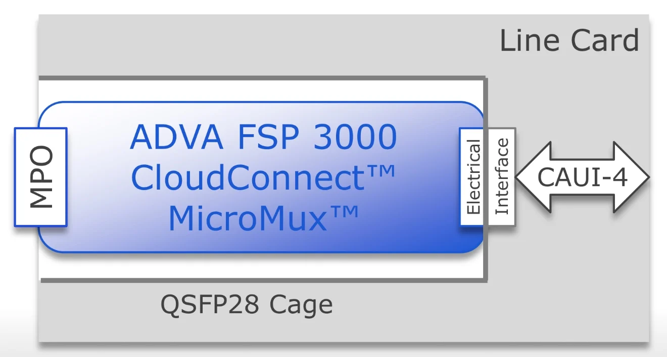
The MicroMux features an MPO connector. For the 10-gigabit products, the MPO connector supports 20 fibres, while for the 40-gigabit products, it is four fibres. At the other end of the QSFP28, that plugs into the platform, sits a CAUI-4 4x25-gigabit electrical interface (see diagram above).
“The key thing is the CAUI-4 interface; this is what makes it all work," says Theodoras.
Inside the MicroMux, signals are converted between the optical and electrical domains while a gearbox IC translates between 10- or 40-gigabit signals and the CAUI-4 format.
Theodoras stresses that the 10-gigabit inputs are not the old 100 Gigabit Ethernet 10x10 MSA but independent 10 Gigabit Ethernet streams. "They can come from different routers, different ports and different timing domains," he says. "It is no different than if you had 10, 10 Gigabit Ethernet ports on the front face plate."
Using the pluggables, a 5-terabit CloudConnect configuration can support up to 520, 10 Gigabit Ethernet ports, according to ADVA Optical Networking.
The first products will be shipped in the third quarter to preferred customers that help in its development while the products will be generally available at the year-end.
ADVA Optical Networking unveiled the MicroMux at OFC 2016, held in Anaheim, California in March. ADVA also used the show to detail its Open Optical Line System demonstration with switch vendor, Arista Networks.
Two years after Microsoft first talked about the [Open Optical Line System] concept at OFC, here we are today fully supporting it
Open Optical Line System
The Open Optical Line System is a concept being promoted by the Internet content providers to afford them greater control of their optical networking requirements.
Data centre players typically update their servers and top-of-rack switches every three years yet the optical transport functions such as the amplifiers, multiplexers and ROADMs have an upgrade cycle closer to 15 years.
“When the transponding function is stuck in with something that is replaced every 15 years and they want to replace it every three years, there is a mismatch,” says Theodoras.
Data centre interconnect line cards can be replaced more frequently with newer cards while retaining the chassis. And the CloudConnect product is also designed such that its optical line shelf can take external wavelengths from other products by supporting the Open Optical Line System. This adds flexibility and is done in a way that matches the work practices of the data centre players.
“The key part of the Open Optical Line System is the software,” says Theodoras. “The software lets that optical line shelf be its own separate node; an individual network element.”
The data centre operator can then manage the standalone CloudConnect Open Optical Line System product. Such a product can take coloured wavelength inputs and even provide feedback with the source platform, so that the wavelength is tuned to the correct channel. “It’s an orchestration and a management level thing,” says Theodoras.
Arista recently added a coherent line card to its 7500 spine switch family.
The card supports six CFP2-ACOs that have a reach of up to 2,000km, sufficient for most data centre interconnect applications, says Theodoras. The 7500 also supports the layer-two MACsec security protocol. However, it does not support flexible modulation formats. The CloudConnect does, supporting 100-, 150- and 200-gigabit formats. CloudConnect also has a 3,000km reach.
 Source: ADVA Optical Networking
In the Open Optical Line System demonstration, ADVA Optical Networking squeezed the Arista 100-gigabit wavelength into a narrower 37.5GHz channel, sandwiched between two 100 gigabit wavelengths from legacy equipment and two 200 gigabit (PM-16QAM) wavelengths from the CloudConnect Quadplex card. All five wavelengths were sent over a 2,000km link.
Implementing the Open Optical Line System expands a data centre manager’s options. A coherent card can be added to the Arista 7500 and wavelengths sent directly using the CFP2-ACOs, or wavelengths can be sent over more demanding links, or ones that requires greater spectral efficiency, by using the CloudConnect. The 7500 chassis could also be used solely for switching and its traffic routed to the CloudConnect platform for off-site transmission.
Spectral efficiency is important for the large-scale data centre players. “The data centre interconnect guys are fibre-poor; they typically only have a single fibre pair going around the country and that is their network,” says Theodoras.
The joint demo shows that the Open Optical Line System concept works, he says: “Two years after Microsoft first talked about the concept at OFC, here we are today fully supporting it.”
Ciena's Tom Mock reflects on a career in telecom
Working for one technology company for so long may be uncommon, says Mock, but not at Ciena: the CTO has clocked 20 years while the CEO boasts 15 years.
 Tom Mock: “I’m about ready to go do something else.”
Mock studied electrical engineering and was at Scientific Atlanta running a product development group before joining Ciena where he crossed over from engineering to marketing. “I’ve been in telecom pretty much my entire career, 35 years worth of telecom,” says Mock. “I’m about ready to go do something else.”
A work colleague says that if there is one word that describes Mock, it is decency: “He has been a key role model of the ‘do the right thing’ culture at Ciena.”
Mock joined Ciena days before the company went public in 1997. He experienced the optical bubble of 1999-2000 and the bust that followed, and just when he thought the company had put that ‘nuclear winter’ behind it, Ciena endured the 2008 global financial crisis.
Now he leaves Ciena as senior vice president of corporate communications. A role, he says, that involves communicating the company's value proposition to the investment community and media, while helping Ciena’s sales staff communicate the company’s brand. The role also involves explaining the significance of the company’s technology: “It is great we can do 16-QAM [quadrature amplitude modulation] on optical, but why is it important?"
When Mock joined Ciena, optical technology in the form of dense wavelength-division multiplexing (DWDM) was starting to be deployed. “You could go to a service provider and say, look, I can increase the capacity of your network by a factor of 16 just by swapping out the bits at the end of your fibre route,” he says.
I remember sitting at my desk looking at stock prices and market capitalisations and realising that a start-up called Corvis ... had a market capitalisation larger than Ford Motor Company
The optical bubble quickly followed. The internet was beginning to change the world, and large enterprises were taking advantage of communication services in new ways. And with it came the inflated expectation that bandwidth demand would grow through the roof. As a result, optical communications became the hottest technology around.
"I remember sitting at my desk looking at stock prices and market capitalisations and realising that a start-up called Corvis, a competitor of ours started by one of the guys that founded Ciena, Dave Huber, had a market capitalisation larger than Ford Motor Company,” says Mock. Ford was the second largest auto manufacturer in the world at the time.
Yet despite all the expected demand for - and speculation in - bandwidth, conversations with Ciena’s customers revealed that their networks were lightly loaded. The inevitable shake-out, once it came, was brutal, particularly among equipment makers. In the end, all that capacity placed in the network was needed, but only from 2006 as the cloud began to emerge and enterprises started making greater use of computing.
“The one positive that came out of the bubble was that a lot of key technologies that enabled things that happened in the late 2000s were developed in that time,” says Mock.
Ciena made several acquisitions during the optical boom, and has done so since; some successful, others less so. Mock says that with most of the good ones, the technology and the market didn't overlap much with Ciena’s.
Speculation didn't work well for the industry in terms of building infrastructure, and it probably doesn't work well in terms of acquisitions.
One acquisition was Cyras Systems for $2.6 billion in 2000, a company developing 10 Gigabit multi-service provisioning platforms and add/ drop multiplexers. But so was Ciena. “That was one example that didn't work so well but if I look at the one that is going the best - Nortel MEN - that was a place where we didn't have as much technology and market overlap,” he says. That makes streamlining products easier and less disruptive for customers.
“The other thing that is important in a good acquisition is a very good understanding of what the end objective is,” he says. “Speculation didn't work well for the industry in terms of building infrastructure, and it probably doesn't work well in terms of acquisitions.”
Making sure the company cultures fit is also key. “In any of these technology acquisitions, it is not just about buying products and markets, it is about buying the capabilities of a workforce,” says Mock. It is important that the new workforce remains productive, and the way that of done is to make sure the staff feel an important part of the company, he says.
Mock highlights two periods that he found most satisfying at Ciena. One was 2006-2008 before the global economic crisis. Ciena was back of a sound financial footing and was making good money. “There was a similar feeling a year to 18 months after the Nortel acquisition” he says. “The integration had been successful, the people were all pointing in the same direction, and employee morale was pretty high.”
You hear about white boxes in the data centre, there are areas in the network where that is going to happen.
What Mock is most proud of in his time at Ciena is the company’s standing. “We do a perception study with our customers every year to 18 months and one of things that comes back is that people really trust the company,” he says. “Our customers feel like we have their best interest at heart, and that is something we have worked very hard to do; it is also the sort of thing you don't get easily.”
Now the industry is going through a period of change, says Mock. If the last 10-15 years can be viewed as a period of incremental change, people are now thinking about how networks are built and used in new ways. It is about shifting to a model that is more in tune with on-demand needs of users, he says: “That kind of shift typically creates a lot of opportunity.” Networks are becoming more important because people are accessing resources in different places and the networks need to be more responsive.
For Ciena it has meant investing in software as more things come under software control. The benefits include network automation and reduced costs for the operators, but it also brings risk. “There are parts of the infrastructure that are likely to become commoditised,” says Mock. “You hear about white boxes in the data centre, there are areas in the network where that is going to happen.”
We both came from small-town, working-class families. Over the years we have probably been more successful that we ever thought we would be, but a lot of that is due to people helping us along the way.
If this is a notable period, why exit now? “It’s a good time for me,” he says. “And there were some things that my wife and I wanted to start looking at.” Mock’s wife retired two years ago and both are keen to give something back.
“We both came from small-town, working-class families,” he says. “Over the years we have probably been more successful that we ever thought we would be, but a lot of that is due to people helping us along the way.”
Mock and his wife were their families’ first generation that got a good professional education. “One of the things that we have taken on board is helping others gain that same sort of opportunity,” he says.
“I’m excited for Tom but will miss having him around,” says his colleague. “Hopefully, in his next phase, he will make the rest of the world a little more decent as well.”