
100 Gig: Is market expectation in need of a reality check?
 “It could easily be ten to 15 years before we see 100Gbps in a big way on the public network side”
Mark Lutkowitz, Telecom Pragmatics
Infonetics Research, in a published White Paper, says that 100Gbps technology will be adopted at a faster rate than 40Gbps was in its first years, and that the 100Gbps market will begin in earnest from 2013. Indeed this could even be sooner if China, which accounts for half of all 40Gbps ports being shipped, moves to 100Gbps faster than expected.
LightCounting, in its research, describes 100 Gbps optical transmission as a transformational networking technology for carriers, and forecasts that sales of 100Gbps dense wavelength division multiplexing (DWDM) line cards will grow to US $2.3 billion by 2015.
But one research firm, Telecom Pragmatics, is sounding a note of caution. It reports that the 40Gbps market is growing nicely and believes that it could be at least a decade before there is a substantial 100Gbps market.
“100G is not going to kill 40G and, if anything, we are bullish about 40G,” says Mark Lutkowitz, principal at Telecom Pragmatics. “I’m not talking about large volume ramp-up of 40G but there is arguably a ramp-up.”
100G Paradox
One reason, not often mentioned, why 40Gbps is being adopted is that it does not require as many networking changes as when 100Gbps technology is deployed. “There is additional compensation [needed] and it is not clear that all the fibres will work with 100G,” says Lutkowitz.
There is also what he calls the ‘100G Paradox’.
The 100Gbps technology will most likely be considered at pinch-points in the operators’ networks. Yet these are the same network pinch-points that were first upgraded to 10Gbps. As a result they are likely to have legacy DWDM systems such that upgrading to 100Gbps is a considerable undertaking. “It is questionable whether these systems can even work with 100G,” he says.
"We really think that 40G should be getting a lot more respect than it is getting”
”When you look at service providers they are willing to put up with a whole amount of pain before they buy something, and they will certainly not forklift electronics or fibre - they will only do that as a last resort.” Another attraction of 40Gbps for the operators is its growing maturity - it is a technology that has been available for several years.
Costs
Telecom Pragmatics also dismisses the argument made by component vendors that the market will move to 100Gbps especially if the cost-per-bit of 100G technology declines faster than expected.
“The first cost [point] is ten times 10G and really you need to get to something like six or seven times [the cost of] 10G before you consider 100G,” says Lutkowitz. But that is not the sole cost. Network protection is needed which means a second system and there are additional networking and operational costs associated with 100Gbps.
Moreover, to whatever extent 40G is deployed, it will put further pressure on 100Gbps as 40Gbps prices decline. “In the 10G market, prices continued to decline and that precluded 40G, now you have 40G - to whatever extent there is deployment - precluding 100G,” says Lutkowitz.
“It could easily be 10 to 15 years before we see 100G in a big way on the public network side,” says Lutkowitz. But he stresses that in the datacenter and for the enterprise, demand for 100Gbps technology will be a different story.
Meanwhile Telecom Pragmatics expects further operator trials at 100Gbps as well as new system announcements from vendors. “But we really think that 40G should be getting a lot more respect than it is getting,” says Lutkowitz.
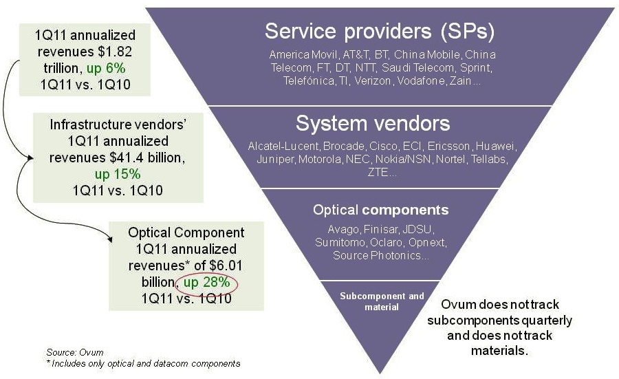
Optical components: The six billion dollar industry
The service provider industry, including wireless and wireline players, is up 6% year-on-year (2Q10 to 1Q11) to reach US $1.82 trillion, according to Ovum. The equipment market, mainly telecom vendors but also the likes of Brocade, has also shown strong growth - up 15% - to reach revenues of over $41.4 billion. But the most striking growth has occurred in the optical components market, up 28%, to achieve revenues of over $6 billion, says the market research firm.
 Source: Ovum
“This is the first time optical components has exceeded six billion since 2001,” says Daryl Inniss, practice leader, Ovum Components. Moreover, the optical component industry growth has continued over six consecutive quarters with the growth being more than 25% for the past four quarters. “None of the other [two] segments have performed in this way,” says Inniss.
Ovum cites three factors accounting for the growth. Fibre-to-the-x (FTTx) is experiencing strong growth while revenues have entered the market from datacom players from the start of 2010. “The [optical] component recovery was led by datacom,” says Inniss. “We speculate that some of that money came from the Googles, Facebooks and Yahoos!.” A third factor accounting for growth has been optical equipment vendors ordering more long lead-time items than needed – such as ROADMs – to secure supply.
 Source: Ovum
The second chart above shows the different market segments normalised since the start of 1999. Shown are the capex spending for optical networking, optical networking equipment revenues, optical components and FTTx equipment spending.
Optical networking spending is some 3.5x that of the components. FTTx equipment revenues are lower than the optical component industry’s and is therefore multiplied by 2.25, while capex is 9.2x that of optical equipment. The peak revenue in 2001 is the optical component revenues during the optical boom.
Several points can be drawn from the normalised chart:
- The strong recent growth in FTTx is the result of the booming Chinese market.
- From 2003 to 2008, the overall market showed steady growth, as illustrated by the best-fit line.
- From 2003 to 2008, capex and optical networking revenues were in line, while two thirds of the optical component revenues were due to this telecom spending.
- From 2010 onwards, components deviated from these two other segments due to the datacom spending from new players and the strong growth in FTTx.
- Once the market crashed in early 2009, optical components, networking and capex all fell. FTTx recovered after only one quarter and was followed by optical components. Optical networking and capex, meanwhile, have still not fully recovered when compared with the underlying growth line.
Capella: Why the ROADM market is a good place to be
The reconfigurable optical add-drop multiplexer (ROADM) market has been the best performing segment of the optical networking market over the last year. According to Infonetics Research, ROADM-based wavelength division multiplexing (WDM) equipment grew 20% from Q2, 2010 to Q1, 2011 whereas the overall optical networking market grew 7%.

“It’s the Moore’s Law: Every two years we are doubling the capacity in terms of channel count and port count”
Larry Schwerin, Capella
The ROADM market has since slowed down but Larry Schwerin, CEO of wavelength-selective-switch (WSS) provider, Capella Intelligent Subsystems, says the market prospects for ROADMs remain solid.
Capella makes WSS products that steer and monitor light at network nodes, while the company’s core intellectual property is closed-loop control. Its WSS products are compact, athermal designs based on MEMS technology that switch and monitor light.
Schwerin compares Capella to a plumbing company: “We clean out pipes and those pipes happen to be fibre-optics ones.” The reason such pipes need ‘cleaning’ – to be made more efficient - is because of the content they carry. “It is bandwidth demand and the nature of the bandwidth which has changed dramatically, that is the fundamental driver here,” says Schwerin.
Increasingly the content is high-bandwidth video and streamed to end-user devices no longer confined to the home, while the video requested is increasingly user-specific. Such changes in the nature of content are affecting the operators’ distribution networks.
“Using Verizon as an example, they are now pushing 50 wavelengths per fibre in the metro,” says Schwerin. Such broad lanes of traffic arrive at network congestion points where certain fibre is partially used while other fibre is heavily used. “What they [operators] need is a vehicle that allows them to dynamically and remotely reassign those wavelengths on-the-fly,” says Schwerin. “That is what the ROADM does.”
Capella attributes strong ROADM sales to a maturing of the technology coupled with a price reduction. The technology also brings valuable flexibility at the optical layer. “It [ROADM] extends the life of the existing infrastructure, avoiding the need for capital to put new fibre in - which is the last thing the operators want to do,” says Schwerin.
$20M funding
Capella raised US $20M in April as part of its latest funding round. The funding is being used for capital expansion and R&D. “We are working on new engine technology, new patentable concepts,” says Schwerin. “We were at Verizon a few weeks ago doing a world-first demo which we will be putting out as a press release.” For now the company will say that the demonstration is research-oriented and will not be implemented within ROADM systems anytime soon.
“You have to be competitive in this market, that is the downfall of our sector. People getting 30 or 40% gross margins and calling that a win – that is not a win - that is why this sector is in trouble”
One investor in the latest funding round is SingTel Innov8, the investment arm of the operator SingTel. Schwerin says it has no specific venture with the operator but that SingTel will gain insight regarding switching technologies due to the investment. “We will sit down with them and talk about their plans for network evolution and what is technologically possible,” says Schwerin, who points out that many of the carriers have lost contact with technologies since they shed their own large, in-house R&D arms.
Cappella offers two 1x9 WSS products and by the end of this year will also offer a 1x20 product. “It’s the Moore’s Law: Every two years we are doubling the capacity in terms of channel count and port count,” says Schwerin.
“We have a reasonable share of design wins shipping in volume - we have thousands of switches deployed throughout the world,” says Schwerin. “We are not of the size of a JDSU or a Finisar but our objective within the next 18 months is to capture enough market share that you would see us as a main supplier of that ilk.”
The CEO stresses that Capella’s presence a decade after the optical boom ended proves it is offering distinctive products. “Our whole business model is about innovation and differentiation,” says Schwerin.
But as a start-up how can Capella compete with a JDSU or a Finisar? “I have these conversations with the carriers: if all they are doing is looking for second or third sourcing of commodity product parts then there is no room for a company like a Capella.”
The key is taking a dumb switch and turning it into a complete wavelength managed solution that can be easily added within the network.
Schwerin also stresses the importance of ROADM specsmanship: wider lightpath channel passbands, lower insertion loss, smaller size, lower power consumption and competitive pricing: “You have to be competitive in this market, that is the downfall of our sector,” says Schwerin. “People getting 30 or 40% gross margins and calling that a win – that is not a win - that is why this sector is in trouble.”
Advanced ROADM features
There has been much discussion in the last year regarding the four advanced attributes being added to ROADM designs: colourless, directionless, contentionless and gridless or CDCG for short.
Interviewing six system vendors late last year, while all claimed they could support CDCG features, views varied as to what would be needed and by when. Meanwhile all the system vendors were being cautious until it was clearer as to what operators needed.
Schwerin says that what the operators really want is a ‘touchless’ ROADM. Capella says its platform is capable of supporting each of the four attributes and that the company has plans for implementing each one. “Just because the carriers say they want it, that doesn’t mean that they are willing to pay for it,” says Schwerin. “And given the intense pricing pressure our system friends are in, they are rightly being cautious.”
Capella says that talking to the carriers doesn’t necessarily answer the issue since views vary as to what is needed. “The one [attribute] that seems clearest of all is colourless,” says Schwerin. And colourless is served using higher-port-count WSSs.
The directionless attribute is more a question of implementation and the good news is that it requires more WSSs, says Schwerin. Contentionless addresses the issue of wavelength blocking and is the most vague, a requirement that has even “faded away a bit”. As for gridless, that may be furthest out as it has ramifications in the network.
Schwerin says that Capella is seeing requests for reduced WSS switching times as well as wavelength tracking, tagging a wavelength whose signature can be identified optically and which is useful for network restoration and when wavelengths are passed between carriers’ networks.
Roadmap
In terms of product plans, Capella will launch a 1x20 WSS product later this year. The next logical step in the development of WSS technology is moving to a solid-state-based design.
“All of the the technologies out there today– liquid crystal, MEMS, liquid-crystal-on-silicon - are all free space [designs],” says Schwerin. “We have a solid-state engine in the middle [of our WSS] and we are down to five photonic-integrated-circuit components so the obvious next stage is silicon photonics.”
Does that mean a waveguide-based design? “Something of that form – it may not be a waveguide solution but something akin to that - but the idea is to get it down to a chip,” says Schwerin. “We are not pure silicon photonics but we are heading that way.”
Such a compact chip-based WSS design is probably five years out, concludes Schwerin.
Further information:
A Fujitsu ROADM discussion with Verizon and Capella – a Youtube 30-min video
Network processors to support multiple 100 Gigabit flows

“We don’t know of any device, announced at least, that comes close to this”
Amir Eyal, EZchip
The NP-5 is noteworthy in integrating within a single chip a full-duplex 100 Gigabit-per-second (Gbps) packet processor and traffic manager. Such integration is important as line cards move from 100Gbps to 400Gbps densities, says Bob Wheeler, senior analyst at The Linley Group.
Target markets
The NP-5 is aimed at router and transport switches platforms that make up the carrier Ethernet switch router (CESR) market. Platforms include packet optical transport switches and edge routers. Infonetics Research forecasts that the total Carrier Ethernet market will grow to US $37bn in 2015 from $26bn in 2010, while the CESR market will double to $20bn by 2015.
EZchip says its main competition is in-house ASIC design teams of the large system vendors. Alcatel-Lucent for example has just announced its FP3 400Gbps network processor. The FP3 is implemented as a three-device chipset made up of a packet processor, traffic manager and a fabric-access chip.
EZchip also believes the device has a role within the data centre. New protocol developments require packet processing that today can only be achieved using a packet processor, it says.
An example is OpenFlow which EZchip supports using its current NP-4 processor. OpenFlow is an academic initiative that allows networking protocols to be explored on existing switch hardware but it is of growing interest to data centre operators. The initiative creates an industry-standard application programming interface (API) to the underlying switch platforms.
The latest OpenFlow version (V1.1) can only be supported using a network processor, says Amir Eyal, EZChip’s vice president of business development. However the data centre is seen as a secondary market for the NP-5. The downside is that the NP-5 and similar network processors targeted at telecoms cost more than switch ASICs from vendors. Only when the functionality of an NPU is needed will vendors pay more.
NP-5 architecture
The chip's main functional blocks are a programmable packet processor and a traffic manager. Also integrated on-chip is an integrated Ethernet switch fabric adaptor, media access controllers (MACs) that support 1, 10, 40 and 100 Gigabit Ethernet (GbE), and a memory controller designed for use with DDR3 external memory to reduce overall system cost. The current NP-4 supports DDR3 and RLDRAM - considerably more expensive than DDR3.
The packet processing is performed using task-optimised processor engines (TOPs). Four styles of TOP engines are used: Two perform classification - parsing, which extracts packet headers and data fields, and searching using look-up tables; and one TOP each for packet modification and packet forwarding.
Each TOP has a 64-bit architecture and processes a single thread. A scheduler allocates a packet to the next available free TOP. EZchip does not disclose the number of TOPs it uses but says that the NP-5 will have almost twice the number used for the NP-4, with the most numerous being the search TOP due to the numerous look-ups needed.
An on-chip ternary content addressable memory (TCAM), meanwhile, supports more sophisticated look-ups and operates in parallel to the simpler TOPs-based searches.
The traffic manager provides bandwidth and guarantees a certain service level performance to particular packet flows. The traffic manager makes decisions when packet congestion occurs based on a given traffic’s priority and its associated rules.
The NP-5 first stores packets in its internal buffer memory before dropping lower-priority packets once memory is full. It is rare that all the input ports are full simultaneously. By taking advantage of the integrated MACs on-chip, up to 24, 10 Gigabit ports can be used to input data. The NP-5 can thus support peak flows of 240Gbps, or a 2.4-to-1 oversubscription rate, equating to a system line card supporting 24-ports at 10Gbps traffic at the same cost as a 10 port-10Gbps design, says EZchip.
The NP-5 will also have four integrated engines. Each engine will support either 12x10GbE, 3x40GbE, 1x100GbE or one Interlaken interface. Two of the four interface engines support 48, 1GbE ports using the QSGMII interface while the remaining two support 12x1GbE ports using the SFI interface.
The QSGMII interface allows a quadrupling of the links by interleaving four ports per link. However an additional external device is needed to break the four interleaved ports into four separate ones. The SFI interface allows a direct connection to a 1GbE optical module.
Also included on the device is an Ethernet fabric adapter that supports 24, 10Gbps (10GBASE-KR) short-reach backplane interfaces.
Device metrics
The 200Gbps NP-5 will be able to process up to 300 million 64byte packets per second. The chip’s power consumption is estimated at 50W. Implemented using a 28nm CMOS process, the device will require 2,401 pins.
What next?
The NP-5 is scheduled to sample year-end 2012. Assuming it takes 18 months to design systems, it will be mid-2014 when NP-5 line cards supporting multiple 100Gbps interfaces are first deployed. EZchip says four or even eight NP-5s could be integrated on a line card, achieving a total packet throughput of 1.6Tbit/s per board.
Meanwhile EZchip’s NP-4 is currently sampling and will ramp in the next few months. Most of the large edge router and switch vendors are designing the NP-4 into their systems, says EZchip.
Further reading:
For more NP-5 detail see the New Electronics article, click here.
Boosting high-performance computing with optics
Part 2: High-performance computing
IBM has adopted optical interfaces for its latest POWER7-based high-end computer system. Gazettabyte spoke to IBM Fellow, Ed Seminaro, about high-performance computing and the need for optics to address bandwidth and latency requirements.
 “At some point when you go a certain distance you have to go to an optical link”
Ed Seminaro, IBM Fellow
IBM has used parallel optics for its latest POWER7 computing systems, the Power 775. The optical interfaces are used to connect computing node drawers that make up the high-end computer. Each node comprises 32 POWER7 chips, with each chip hosting eight processor cores, each capable of running up to four separate programming tasks or threads.
Using optical engines, each node – a specialised computing card - has a total bandwidth of 224, 120 Gigabit-per-second (12x10Gbps) VCSEL-based transmitters and 224, 120Gbps receivers. The interfaces can interconnect up to 2,048 nodes, over half a million POWER7 cores, with a maximum network diameter of only three link hops.
IBM claims that with the development of the Power 775, it has demonstrated the superiority of optics over copper for high-end computing designs.
High-performance computing
Not so long ago supercomputers were designed using exotic custom technologies. Each company crafted its own RISC microprocessor that required specialised packaging, interconnect and cooling. Nowadays supercomputers are more likely to be made up of aggregated servers – computing nodes - tied using a high-performance switching fabric. Software then ties the nodes to appear to the user as a single computer.
But clever processor design is still required to meet new computing demands and steal a march on the competition, as are ever-faster links – interconnect bandwidth - to connect the nodes and satisfy their growing data transfer requirements.
High-performance computing (HPC) is another term used for state-of-the-art computing systems, and comes in many flavours and deployments, says Ed Seminaro, IBM Fellow, power systems development in the IBM Systems & Technology Group.
“All it means is that you have a compute-intensive workload – or a workload combining compute and I/O [input-output] intensive aspects," says Seminaro. "These occur in the scientific and technical computing world, and are increasingly being seen in business around large-scale analytics and so called ‘big data’ problem sets.”
Within the platform, the computer’s operating system runs on a processor or a group of processors connected using copper wire on a printed circuit board (PCB), typically a few inches apart, says Seminaro
The processor hardware is commonly a two-socket server: two processor modules no more than 10 inches apart. The hardware can run a single copy of the operating system – known as an image - or many images.
Running one copy of the operating system, all the memory and all the processing resource are carefully managed, says Seminaro. Alternatively an image can be broken into hundreds of pieces with a copy of the operating system running on each. “That is what virtualisation means,” says Seminaro. The advent of virtualisation has had a significant impact in the design of data centres and is a key enabler of cloud computing (Add link).
“The biggest you can build one of these [compute nodes] is 32 sockets – 32 processor chips - which may be as much as 256 processor cores - close enough that you can run them as what we call a single piece of hardware,” says Seminaro. But this is the current extreme, he says, the industry standard is two or four-socket servers.
That part is well understood, adds Seminaro, the challenge is connecting many of these hardware pieces into a tightly-coupled integrated system. This is where system performance metrics of latency and bandwidth come to the fore and why optical interfaces have become a key technology for HPC.
Latency and bandwidth
Two data transfer technologies are commonly used for HPC: Ethernet LAN and Infiniband. The two networking technologies are also defined by two important performance parameters: latency and bandwidth.
Using an Ethernet LAN for connectivity, the latency is relatively high when transferring data between two pieces of hardware. Latency is the time it takes before requested data starts to arrive. Normally when a process running on hardware accesses data from its local memory the latency is below 100ns. In contrast, accessing data between nodes can take more than 100x longer or over 10 microseconds.
For Infiniband, the latency between nodes can be under 1 microsecond, still 10x worse than a local transfer but more than 10x better than Ethernet. “Inevitably there is a middle ground somewhere between 1 and 100 microsecond depending on factors such as the [design of the software] IP stack,” says Seminaro.
If the amount of data requested is minor, the transfer itself typically takes nanoseconds. If a large file is requested, then not only is latency important – the time before asked-for data starts arriving – but also the bandwidth dictating overall file transfer times.
To highlight the impact of latency and bandwidth on data transfers, Seminaro cites the example of a node requesting data using a 1 Gigabit Ethernet (GbE) interface, equating to a 100MByte-per-second (MBps) transfer rate. The first bit of data requested by a node arrives after 100ns but a further second is needed before the 100MB file arrives.
A state-of-the-art Ethernet interface is 10GbE, says Seminaro: “A 4x QDR [quad data rate] Infiniband link is four times faster again [4x10Gbps].” The cost of 4x QDR Infiniband interconnect is roughly the same as for 10GbE, so most HPC systems either use 1GbE, for lowest cost networking, or 4x QDR Infiniband, when interconnect performance is a more important consideration. Of the fastest 500 computing systems in the world, over 425 use either 1GbE or Infiniband, only 11 use 10GbE. The remainder use custom or proprietary interconnects, says IBM.
The issue is that going any distance at these speeds using copper interfaces is problematic. “At some point when you go a certain distance you have to go to an optical link,” says Seminaro. “With Gigabit Ethernet there is copper and fibre connectivity; with 10GbE the standard is really fibre connectivity to get any reasonable distance.”
Copper for 10GbE or QDR Infiniband can go 7m, and using active copper cable the reach can be extended to 15m. Beyond that it is optics.
“We have learned that we can do a very large-scale optical configuration cost effectively. We had our doubts about that initially”
Ed Seminaro
The need for optics
Copper’s 7m reach places an upper limit on the number of computing units – each with 32 processor nodes - that can be reached. “To go beyond that, I’m going to have to go optical,” says Seminaro.
But reach is not the sole issue. The I/O bandwidth associated with each node is also a factor. “If you want an enormous amount of bandwidth out of each of these [node units], it starts to get physically difficult to externalise from each that many copper cables,” says Seminaro.
Many data centre managers would be overjoyed to finally get rid of copper, adds Seminaro, but unfortunately optical costs more. This has meant people have pushed to keep copper alive, especially for smaller computing clusters.
People accept how much bandwidth they can get between nodes using technologies such as QDR linking two-socket servers, and then design the software around such performance. “They get the best technology and then go the next level and do the best with that,” says Seminaro. “But people are always looking how they can increase the bandwidth dramatically coming out of the node and also how they can make the node more computationally powerful.” Not only that, if the nodes are more powerful, fewer are needed to do a given job, he says.
What IBM has done
The IBM’s Power 775 computer system is a sixth generation design that started in 2002. The Power 775 is currently being previewed and will be generally available in the second half of 2011, says IBM.
At its core is a POWER7 processor, described by Seminaro as highly flexible. The processor can tackle various problems from commercial applications to high-performance computing and which can scale from one processing node next to the desk to complete supercomputer configurations.
Applications the POWER7 is used for include large scale data analysis, automobile and aircraft design, weather prediction, and oil exploration, as well as multi-purpose computing systems for national research labs.
In the Power 775, as mentioned, each node has 32 chips comprising 256 cores, and each core can process four [programming] threads. “That is 1,024 threads – a lot of compute power,” says Seminaro, who stresses that the number of cores and the computing capability of each thread are important, as is the clock frequency at which they are run. These threads must access memory and are all tightly coupled.
“That is where it all starts: How much compute power can you cram in one of these units of electronics,” says Seminaro. The node design uses copper interconnect on a PCB and in placed into a water-cooled drawer to ensure a relatively low operating temperature, which improves power utilisation and system reliability.
“We have pulled all the stops out with this drawer,” says Seminaro. “It has the highest bandwidth available in a generally commercially available processor – we have several times the bandwidth of a typical computing platform at all levels of the interconnect hierarchy.”
To connect the computing nodes or drawers, IBM uses optical interfaces to achieve a low latency, high bandwidth interconnect design. Each node uses 224 optical transceivers, with each transceiver consisting of an array of 12 send and 12 receive 10Gbps lanes. This equates to a total bandwidth per 2U-high node of 26.88+26.88 Terabit-per-second.
“That is equivalent to 2,688 10Gig Ethernet connections [each way],” says Seminaro. “Because we have so many links coming out of the drawer it allows us to connect a lot of drawers directly to each other.”
In a 128-drawer system, IBM has sufficient number of ports and interconnect bandwidth to link each drawer to every one of the other 127. Using the switching capacity within the drawer, the Power 775 can be further scaled to build systems of up to 2,048 node drawers, with up to 524,288 POWER7 cores.
IBM claims one concern about using optics was cost. However working with Avago Technologies, the supplier of the optical transceivers, it has been able to develop the optical-based systems cost-effectively (see 'Parallel Optics' section within OFC round-up story) . “We have learned that we can do a very large-scale optical configuration cost effectively,” says Seminaro. “We had our doubts about that initially.”
IBM also had concerns about the power consumption of optics. “Copper is high-power but so is optics,” says Seminaro. “Again working with Avago we’ve been able to do this at reasonable power levels.” Even for very short 1m links the power consumption is reasonable, says IBM, and for longer reaches such as connecting widely-separated drawers in a large system, optical interconnect has a huge advantage, since the power required for an 80m link is the same as for a 1m link.
Reliability was also a concern given that optics is viewed as being less reliable than copper. “We have built a large amount of hardware now and we have achieved outstanding reliability,” says Seminaro.
IBM uses 10 out of the 12 lanes - two lanes are spare. If one lane should fail, one of the spare lanes is automatically configured to take its place. Such redundancy improves the failure rate metrics greatly and is needed in systems with a large number of optical interconnects, says Seminaro.
IBM has also done much work to produce an integrated design, placing the optical interfaces close to its hub/switch chip and reducing the discrete components used. And in a future design it will use an optical transceiver that integrates the transmit and receive arrays. IBM also believes it can improve the integration of the VCSEL-drive circuitry and overall packaging.
What next?
For future systems, IBM is investigating increasing the data rate per channel to 20-26Gbps and has already designed the current system to be able to accommodate such rates.
What about bringing optics within the drawer for chip-to-chip and even on-chip communications?
“There is one disadvantage to using optics which is difficult to overcome and that is latency,” says Seminaro. “You will always have higher latency when you go optics and a longer time-of-flight than you have with copper.” That’s because converting from wider, slower electrical buses to narrower optical links at higher bit rate costs a few cycles on each end of the link.
Also an optical signal in a fibre takes slightly longer to propagate, leading to a total increase in propagation delay of 1-5ns. “When you are within that drawer, especially when you are in some section of that drawer say between four chips, the added latency and time-of–flight definitely hurts performance,” says Seminaro.
IBM does not rule out such use of optics in the future. However, in the current Power 775 system, using optical links to interconnect the four-chip processor clusters within a node drawer does not deliver any processing performance advantage, it says.
But as application demands rise, and as IBM’s chip and package technologies improve, the need for higher bandwidth interconnect will steadily increase. Optics within the drawer is only a matter of time.
Further reading
Part 1: Optical Interconnect: Fibre-to-the-FPGA
Get on the Optical Bus, IEEE Spectrum, October 2010.
Optical networking market in rude health
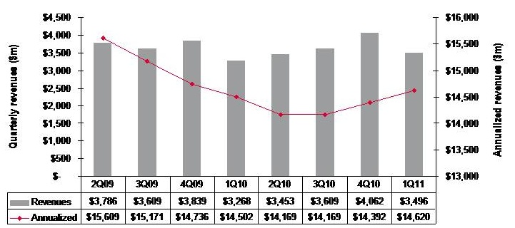 Quarterly market revenues, global optical networking (1Q 2011). Source: Ovum
Despite recent falls in optical equipment makers’ stock, the optical networking market remains in good health with analysts predicting 6-7% growth in 2011.
For Andrew Schmitt, directing analyst for optical at Infonetics Research, unfulfilled expectations are nothing new. Optical networking is a market of single-digit yearly growth yet in the last year certain market segments have grown above average: spending on ROADM-based wavelength division multiplexing (WDM) optical network equipment, for example, has grown 20% since the first quarter of 2010.
“Every few years people get this expectation that there is going to be this hockey stick [growth] and it is not,” says Schmitt. “There has been a lot of Wall Street money moving into this sector in the latter part of 2010 and first part of this year and they have just had their expectations reset, but operationally the industry is very healthy.”

“Nothing in this business changes quickly but the pace of change is starting to accelerate”
Andrew Schmitt, Infonetics Research
But Schmitt acknowledges that there is industry concern about the market outlook. “There have been lots of client calls in the first half of the year wanting to talk numbers,” says Schmitt. “When the market is growing rapidly there is no need for such calls but when it is uncertain, customers put more time into understanding what is going on.”
Both Infonetics and market research firm Ovum say the optical networking market grew 7% globally in the last year (2Q10 to 1Q11).
Ovum says the market reached US $3.5bn in the first quarter of 2011 and it expects 6% growth this year. “Most of the growth will come from North America—general recovery, stimulus-related spending, and LTE (Long Term Evolution)-inspired spending; and from South and Central America mostly mobile and fixed broadband-related,” says Dana Cooperson, network infrastructure practice leader at Ovum.
Ovum also notes that optical networking annualised spending for the last four quarters (2Q10-1Q11) finally went into the black with 1% growth, to reach $14.6bn. Annualised share figures are a strong indicator of longer-term market trends, says Ovum.
Market growth
Factors accounting for the growth include optical equipment demand for mobile and broadband backhaul. Carriers are also embarking on a multi-year optical upgrade to 40 and 100 Gigabit transmission over Optical Transport Network (OTN) and ROADM-based networks. Infonetics notes that ROADM spending in particular set a new high in the first quarter, rising 4% sequentially.
Ovum expects overall growth to come from metro and backbone WDM markets and from LTE. “For metro it is a combination of new builds, as DWDM continues to take over the metro core from SONET/SDH, and expansions of ROADM and 40 Gigabit,” says Cooperson. “For backbone it is a combination of retrofits for 40 and 100 Gigabit and overbuilds with 40 and 100 Gigabit coherent-optimised systems.”
Many operators are also looking at OTN switching and how it can help with network efficiency and manageability, she says, while mobile backhaul continues to be a hot spot as well at the access end of the network.
The Americas are the regions accounting for market growth whereas in Asia-Pacific and Europe, Middle East and Africa the spending remains flat.
“We’re not as bullish on Europe as I’ve heard some others are,” says Cooperson. “We expected China to slow down as capital intensities in the 34-35% seen in 2008 and 2009 were unsustainable. We saw the cooling down a bit earlier in 2010 than we had expected, but it did cool down and will continue to.”
Ovum expects Asia-Pacific as a whole to be moribund. But at least the pullbacks in China will be countered by slow growth in Japan and a big upsurge in India after a huge decline last year due to delayed 3G-related builds among other issues.
Outlook
Ovum is optimistic about the optical networking market due to continued competitive pressures and traffic growth. “We don’t think traffic growth can just continue without attention to the underlying issues related to revenue pressure, regardless of competitive pressures,” says Cooperson. “But newer optical and packet systems offer significant improvements over the old in terms of power efficiency, manageability, and of course 40 and 100 Gigabit coherent and ROADM features.”
“Most of the growth will come from North America"
Dana Cooperson, Ovum.
Many networks worldwide are also due for a core infrastructure update to benefit capacity and efficiency while many other operators are upgrading their access networks for mobile backhaul and enterprise Ethernet services.
Schmitt stresses that while it is right to talk about a 'core reboot', there are all sorts of operators that make up the market: the established carriers, those focussed on Layer 2 and Layer 3 transport, dark fibre companies and cable companies.
“Everyone has a different business so there is not a whole lot of group-think in this industry,” says Schmitt. “So when you talk about a transition to 40 and 100 Gigabit, some carriers will make that transition earlier than others because the nature of their business demands it.”
However, there are developments in equipment costs that are leading to change. “Once you get out to 2013-14, 100 Gigabit [transport] looks really good relative to 40 Gigabit and tunable XFPs at 10 Gigabit look really, really good,” says Schmitt, who believes these are going to be two dominating technologies. “People are going to use 100 Gigabit and when they can afford to throw more 10 Gigabit at the [capacity] problem, in shorter metro and regional spans, they will use tunable XFPs,” he says. “That is a whole new level in terms of driving down cost at 10 Gigabit that people haven’t factored in yet.”
Pacier change
The move to 100 Gigabit will not lead to increased spending, stresses Schmitt. Rather its significance is as a ‘mix shift’: The adoption of 100 Gigabit will shift spending from older systems to newer ones so that the technology is interesting in terms of market share shift rather than by growing overall revenues.
That said, there are areas of optical spending where capital expenditure (capex) is growing faster than the single-digit trend. These include certain competitive telco providers and dark fibre providers like AboveNet, TimeWarner Telecom and Colt. “You look at their capex year-over-year and it is increasing in some cases more over 20% a year,” says Schmitt.
He also notes that while the likes of Google, Yahoo, Microsoft and Apple do not spend on optical equipment as much as established operators such as Verizon or AT&T, their growth rate is higher. “There are sectors of the market that are growing quickly, and competition that are positioned to service those sectors successfully are going to see above-trend growth,” says Schmitt.
He highlights three areas of innovations - ‘big vectors’- that are going to change the business.
One is optical transport's move away from simple on-off keying signalling that opens up all kinds of innovation. Another is the shift in the players buying optical equipment. “A lot more of the R&D is driven by the AboveNets, Time Warners, Comcasts and the Googles and less by the old time PTTs,” says Schmitt. “That is going to change the way R&D is done.”
The third is photonic integration which Schmitt equates to the very early state of the electronics business. While Infinera has done some interesting things with integration, its latest 500 Gigabit PIC (photonic integrated circuit) is a big leap in density, he says: “It will be interesting if that sort of technology crosses over into other applications such as short- and intermediate-reach applications.”
“Nothing in this business changes quickly but the pace of change is starting to accelerate,” says Schmitt. “These three things, when you throw them together in a pot, are going to result in some unpredictable outcomes.”
LTE-Advanced - a mind map

A mind map of the emerging 3GPP LTE Release 10 standard, also known as LTE-Advanced. For a pdf, click here
R&D: At home or abroad?
 Omer Industrial Park in the Negev, Israel - the location of ECI Telecom's latest R&D centre.
Chaim Urbach likes working at the Omer Industrial Park site. Normally located at ECI’s headquarters in Petah Tikva, he visits the Omer site - some 100km away - once or twice a week and finds he is more productive there. Urbach employs an open door policy and has fewer interruptions at the Omer site since engineers are focussed solely on R&D work.
ECI set up its latest R&D centre in May 2010 with a staff of ten. “In 2009 we realised we needed more engineers,” says Urbach. One year on the site employs 150, by the end of the year it will be 200, and by year-end 2012 the company expects to employ 300. ECI has already taken one unit at the Industrial Park and its operations have already spilt over into a second building.
Urbach says that the decision to locate the new site in the south of Israel was not straightforward.
The company has 1,300 R&D staff, with research centres in the US, India and China. Having a second site in Israel helps in terms of issues of language and time zones but employing an R&D engineer in Israel is several times more costly than an engineer in India or China.
 The photos on the wall are part of the winning entries in an ECI company-wide photo competition.
But the Israeli Government’s Office of the Chief Scientist (OCS) is keen to encourage local high-tech ventures and has helped with the funding of the site. In return the backed-venture must undertake what is deemed innovative research with the OCS guaranteed royalties from sales of future telecom systems developed at the site.
One difficulty Urbach highlights is recruiting experienced hardware and software engineers given that there are few local high-tech companies in the south of the country. Instead ECI has relocated experienced engineering managers from Petah Tikva, tasked with building core knowledge by training graduates from nearby Ben-Gurion University and from local colleges.
Work on the majority of ECI’s new projects in being done at the Omer site, says Urbach. Projects include developing GPON access technology for a BT tender as well as extending its successful XDM hybrid+ SDH to all-IP transport platform, which has over 30% market share in India. ECI is undertaking the research on one terabit transmission using OFDM technology, part of the Tera Santa Consortium, at its HQ.
 “We realised we needed more engineers”
Chaim Urbach, ECI Telecom
Urbach admits it is a challenge to compete with leading Far Eastern system vendors on cost and given their R&D budgets. But he says the company is focussed on building innovative platforms delivered as part of a complete solution. “We do not just provide a box,” says Urbach. “And customers know if they have a problem, we go the extra mile to solve it.”
 Omer Industrial Park
The company is highly business oriented, he says, delivering solutions that fit customers’ needs. “Over 95% of all systems ECI has developed have been sold,” he says.
Urbach also argues that Israeli engineers are suited to R&D. “Engineers don’t do everything by the book,” he says. “And they are dedicated and motivated to succeed.”
For more photos of the Omer Industrial Park, click here
Fibre-to-the-FPGA
Part 1: FPGAs
Programmable logic chip vendor Altera is developing FPGAs with optical interfaces. But is there a need for such technology and how difficult will it be to develop?
FPGAs with optical interfaces promise to simplify high-speed interfacing between and within telecom and datacom systems. Such fibre-based FPGAs, once available, could also trigger novel system architectures. But not all FPGA vendors believe optical-enabled FPGAs’ time has come, arguing that cost and reliability hurdles must be overcome for system vendors to embrace the technology

“One of the advantages of using optics is that you haven’t got to throw your backplanes away as [interface] speeds increase.”
Craig Davis, Altera
Altera announced in March that it is developing FPGAs with optical interfaces. The FPGA vendor has yet to detail its technology demonstrator but says it will do so later this year. Altera describes the advent of optically-enabled FPGAs as a turning point, driven by the speed-reach tradeoff of electrical interfaces coupled with the rising cost of elaborate printed circuit board (PCB) materials needed for the highest speed interfaces.
Interface speeds continue to rise. The Interlaken interface has a channel rate of up to 6.375 Gigabit-per-second (Gbps) while the Gen 3.0 PCI Express standard uses 8.0 Gbps lanes. Meanwhile 16 Gigabit Fibre Channel standard operates at 14.1 Gbps while 100 Gigabit interfaces for Ethernet and line-side optical transport are moving to a four-channel electrical interface that almost doubles the lane rates to 25-28 Gbps. The CFP2 optical module for 100 Gigabit, to be introduced in 2012, will use the four-channel electrical interface.
Copper interfaces such channel speeds but at the expense of reach. Craig Davis, senior product marketing engineer at Altera, cites the 10GBASE-KR 10Gbps backplane standard as an example of the bandwidth-reach the latest FPGAs can achieve: 40 inches including the losses introduced by the two connectors at each end.

“Our interactions with our customers are primarily for products that are not going to see the light of day for several years”
Panch Chandrasekaran, Xilinx
Work is being undertaken to development very short reach electrical interfaces at 28Gbps for line cards and electrical backplanes. “You are talking 4 to 6 inches of trace to a CFP2 module or a chip-to-chip interface,” says Panch Chandrasekaran, Xilinx’s senior product marketing manager, high-speed serial I/O. “Honestly, this is going to be a challenge but we usually figure out a way how to do things.”
The faster the link, the more energy has to be put into the signals and the more losses you have on the board, says Davis: “Signal integrity aspects also get more difficult, the costs go up as does the power consumption.”
According to Altera, signal losses increase 3.5x going from 10 to 30Gbps. To match the losses at 10Gbps when operating at these higher speeds, complex PCB materials such as N4000-13 EP SI and Megtron 6 are needed rather than the traditional FR4 design. However, the cost of designing and manufacturing such PCBs can rise by five-fold.
In contrast, using an optically-enabled FPGA simplifies PCB design. “For traditional chip-to-chip on a line card, optics does have a benefit because you can trade off the number of layers on a PCB,” says Davis. Such an optical-based design also offers future-proofing. “A lot of the applications we’ll be looking to support are across backplanes and between shelves,” says Davis. “One of the advantages of using optics is that you haven’t got to throw your backplanes away as [interface] speeds increase.”
FPGAs with optical interfaces also promise new ways to design systems. Normally when one line card talks to another on different shelves it is via a switch card on each shelf. Using an FPGA with an optical interface, the cards can talk directly. “People are looking at this,” says Davis. “You could take that to the extreme and go to the next cabinet which makes a much easier system design.”
Altera says vendors are interested in optical-enabled FPGAs for storage systems. Here interlinked disk drives require multiple connectors between boards. “There is an argument that it becomes a simpler system design with one FPGA taking directly to another or one chip directly to another,” says Davis “The more advanced R&D groups within certain companies are investigating the best route forward.”
But while FPGA companies agree that optical interfaces will be needed, there is no consensus on timing. “Xilinx has been looking at this technology for a while now,” says Chandrasekaran. “There is a reason why we haven’t announced it: we have a little while to go before key ecosystem and technology questions are answered.”
The mechanical and reliability issues of systems are stringent and the optical option must prove that it can deliver what is needed, says Chandrasekaran. “It is possible to do at the moment but the cost and reliability equation hasn’t been fully solved.”
Xilinx also says that while it is discussing the technology with customers, the requirement for such FPGA-based optical interfaces is some way off. “Our interactions with our customers are primarily for products that are not going to see the light of day for several years,” says Chandrasekaran
“Customers are always excited to hear about integration play,” says Gilles Garcia, director, wired communications business unit at Xilinx. But ultimately end customers care less about the technology as long as the price, power and board real-estate requirements are met. “What we are seeing with this [optical-enabled FPGA] technology is that it is not answering the requirements we are seeing from our large customers that are looking for their next-generation systems,” says Garcia
FPGA vendor Tabula also questions the near-term need for such technology. Alain Bismuth, vice president of marketing at Tabula, says nearly all the ports shipped today are at speeds of 10Gbps and below. Even in 2014, the number of 40Gbps ports forecast will only number 650,000, he says.
For Bismuth, two things must happen before optically-enabled FPGAs become commonplace. “You can build them in high volumes reliably and with good yields without incurring higher costs than a separate, discrete [FPGA and optical module] solution,” says Bismuth. “Second, the emergence in interesting volume of networks at 100 Gig and beyond to justify the integration effort.” Such networks are emerging at a “fairly slow pace”, he says.
Meanwhile Altera’s development work continues apace. “We are working with partners to develop the system and we will be demonstrating the optics-on-a-chip in Q4,” says Bob Blake, corporate and product marketing manager, Altera Europe. Altera says its packaged FPGA and optical interface will support short reach links up to 100m and be based on multimode fibre. “All we have announced is that the optical interface will be on the package and it will connect into the FPGA,” says Davis.
The technology will also use 10Gbps optical interface yet the company has detailed that its Stratix V FPGA family supports electrical transceivers at 28Gbps. “The optical interface can go higher than that [10Gbps] so in future we can target 28Gbps and beyond,” says Davis.
Optical partners
Optical component and transceiver firms such as Avago Technologies, Finisar and Reflex Photonics all have parallel optical devices - optical engines - that support up to 12 channels at 10Gbps. Avago’s MicroPod 12x10Gbit/s optical engine measures 8x8mm, for example.
None of the optical vendors would comment on its involvement with Altera’s optical-enabled FPGA.
Avago Technologies says that as FPGA interface speeds move to 10 Gbps and beyond, its customers are finding they need to move from copper to optical interfaces to maintain bandwidth for board, chassis, and system-level interconnect. “In line with this announcement from Altera, we are investing the time to verify Avago optical modules with FPGA SERDES blocks to ensure that FPGA users can design optical interfaces with confidence,” says Victor Krutul, director of marketing for fibre optic products at Avago.
Finisar too only talks about general trends. “We are seeing many technology leaders moving optics further onto the board and deeper into the system,” says Katharine Schmidtke, director of strategic marketing for Finisar. “This approach offers a number of advantages including improving signal integrity and reducing power consumption on copper traces at higher bandwidths.”
Reflex Photonics says that it has the technology and products to realise optically-enabled IC packages. “We are working with more than one IC company to bring optically-enabled IC packages to market,” says Robert Coenen, vice president, sales and marketing at Reflex.
For Coenen, FPGAs represent the first step in bringing optics to the IC package: “Due to their penetration into niche markets, FPGAs make the most sense to create what will ultimately be a huge market in optically-enabled IC packages.”
Coenen stresses that optics to the IC package is a significant shift in how optical links are used and so it will take time for this application to take hold. However, as the cost per bit decreases, optics will start being used in additional applications including switch ASICs, microprocessors and graphics processors.
“The beauty of an MT-terminated ribbon fiber optical connection at the edge of the package is that this solution allows designers to use the additional high-speed optical connectivity without having to drastically change their design practices,” says Coenen. This is not the case with technologies such as PCB optical waveguides or free-space optical communication.
“I believe the Altera announcement is just the first in what will be many announcements of optical-to-the-IC-package technology in the coming year or two,” says Coenen.
Further reading
- Briefing Part 2: Boosting high performance computing with optics
- Altera White Paper: Overcome Copper Limits with Optical Interfaces
- Xilinx's 400 Gigabit Ethernet FPGA
- The InfiniBand roadmap gets redrawn
Terabit Consortium embraces OFDM
 “This project is very challenging and very important”
Shai Stein, Tera Santa Consortium
Given the continual growth in IP traffic, higher-speed light paths are going to be needed, says Shai Stein, chairman of the Tera Santa Consortium and ECI Telecom’s CTO: “If 100 Gigabit is starting to be deployed, within five years we’ll start to see links with tenfold that capacity, meaning one Terabit.”
The project is funded by the seven participating firms and the Israeli Government. According to Stern, the Government has invested little in optical projects in recent years. “When we look at the [Israeli] academies and industry capabilities in optical, there is no justification for this,” says Stern. “We went with this initiative in order to get Government funding for something very challenging that will position us in a totally different place worldwide.”
Orthogonal frequency division multiplexing
OFDM differs from traditional dense wavelength division multiplexing (DWDM) technology in how fibre bandwidth is used. Rather than sending all the information on a lightpath within a single 50 or 100GHz channel – dubbed single-carrier transmission – OFDM uses multiple narrow carriers. “Instead of using the whole bandwidth in one bulk and transmitting the information over it, [with OFDM] you divide the spectrum into pieces and on each you transmit a portion of the data,” says Stein. “Each sub-carrier is very narrow and the summation of all of them is the transmission.”
“Each time there is a new arena in telecom we find that there is a battle between single carrier modulation and OFDM; VDSL began as single carrier and later moved to OFDM,” says Amitai Melamed, involved in the project and a member of ECI’s CTO office. “In the optical domain, before running to [use] single-carrier modulation as is currently done at 100 Gigabit, it is better to look at the OFDM domain in detail rather than jump at single-carrier modulation and question whether this was the right choice in future.”
OFDM delivers several benefits, says Stern, especially in the flexibility it brings in managing spectrum. OFDM allows a fibre’s spectrum band to be used right up to its edge. Indeed Melamed is confident that by adopting OFDM for optical, the spectrum efficiency achieved will eventually match that of wireless.
“OFDM is very tolerant to rate adaptation.”
Amitai Melamed, ECI Telecom
The technology also lends itself to parallel processing. “Each of the sub-carriers is orthogonal and in a way independent,” says Stern. “You can use multiple small machines to process the whole traffic instead of a single engine that processes it all.” With OFDM, chromatic dispersion is also reduced because each sub-carrier is narrow in the frequency domain.
Using OFDM, the modulation scheme used per sub-carrier can vary depending on channel conditions. This delivers a flexibility absent from existing single-carrier modulation schemes such as quadrature phase-shift keying (QPSK) that is used across all the channel bandwidth at 100 Gigabit-per-second (Gbps). “With OFDM, some of the bins [sub-carriers] could be QPSK but others could be 16-QAM or even more,” says Melamed.
The approach enables the concept of an adaptive transponder. “I don’t always need to handle fibre as a time-division multiplexed link – either you have all the capacity or nothing,” says Melamed. “We are trying to push this resource to be more tolerant to the media: We can sense the channels' and adapt the receiver to the real capacity.” Such an approach better suits the characteristics of packet traffic in general he says: “OFDM is very tolerant to rate adaptation.”
The Consortium’s goal is to deliver a 1 Terabit light path in a 175GHz channel. At present 160, 40Gbps can be crammed within the a fibre's C-band, equating to 6.4Tbps using 25GHz channels. At 100Gbps, 80 channels - or 8Tbps - is possible using 50GHz channels. A 175GHz channel spacing at 1Tbps would result in 23Tbps overall capacity. However this figure is likely to be reduced in practice since frequency guard-bands between channels are needed. The spectrum spacings at speeds greater than 100Gbps are still being worked out as part of ITU work on "gridless" channels (see OFC announcements and market trends story).
ECI stresses that fibre capacity is only one aspect of performance, however, and that at 1Tbps the optical reach achieved is reduced compared to transmissions at 100Gbps. “It is not just about having more Gigabit-per-second-per-Hertz but how we utilize the resource,” says Melamed. “A system with an adaptive rate optimises the resource in terms of how capacity is managed.” For example if there is no need for a 1Tbps link at a certain time of the day, the system can revert to a lower speed and use the spectrum freed up for other services. Such a concept will enable the DWDM system to be adaptive in capacity, time and reach.
Project focus
The project is split between digital and analogue, optical development work. The digital part concerns OFDM and how the signals are processed in a modular way.
The analogue work involves overcoming several challenges, says Stern. One is designing and building the optical functions needed for modulation and demodulation with the accuracy required for OFDM. Another is achieving a compact design that fits within an optical transceiver. Dividing the 1Tbps signal into several sub-bands will require optical components to be implemented as a photonic integrated circuit (PIC). The PIC will integrate arrays of components for sub-band processing and will be needed to achieve the required cost, space and power consumption targets.
Taking part in the project are seven Israeli companies - ECI Telecom, the Israeli subsidiary of Finisar, MultiPhy, Civcom, Orckit-Corrigent, Elisra-Elbit and Optiway- as well as five Israeli universities.
 Two of the companies in the Consortium
“There are three types of companies,” says Stern. “Companies at the component level – digital components like digital signal processors and analogue optical components, sub-systems such as transceivers, and system companies that have platforms and a network view of the whole concept.”
The project goal is to provide the technology enablers to build a terabit-enabled optical network. A simple prototype will be built to check the concepts and the algorithms before proceeding to the full 1Terabit proof-of-concept, says Stern. The five Israeli universities will provide a dozen research groups covering issues such as PIC design and digital signal processing algorithms.
Any intellectual property resulting from the project is owned by the company that generates it although it will be made available to any other interested Consortium partner for licensing.
Project definition work, architectures and simulation work have already started. The project will take between 3-5 years but it has a deadline after three years when the Consortium will need to demonstrate the project's achievements. “If the achievements justify continuation I believe we will get it [a funding extension],” says Stern. “But we have a lot to do to get to this milestone after three years.
Project funding for the three years is around US $25M, with the Israeli Office of the Chief Scientist (OCS) providing 50 million NIS (US $14.5M) via the Magnet programme, which ECI says is “over half” of the overall funding.
Further reading: