
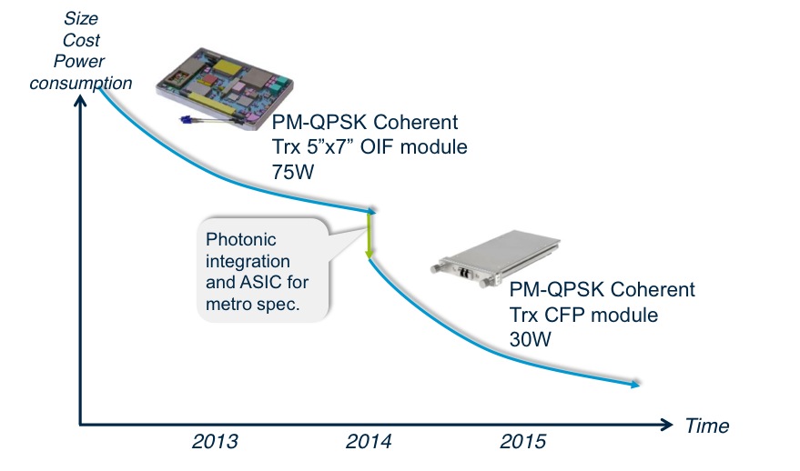
ClariPhy samples a 200 Gigabit coherent DSP-ASIC
The CL20010 is the first of ClariPhy's LightSpeed-II family of coherent digital signal processing ASICs (DSP-ASICs), manufactured using a 28nm CMOS process. "We believe it is the first 28nm standard product, and leaps ahead of the current generation [DSP-ASIC] devices," says Paul Voois, co-founder and chief strategy officer at ClariPhy.
 Paul Voois
ClariPhy has been shipping its 40 Gigabit coherent CL4010 LightSpeed chip since September 2011. Customers using the device include optical module makers Oclaro, NEC and JDSU. "We continue to go into new deployments but it is true that the 40 Gig market is not growing like the 100 Gig market," says Voois.
With the CL20010, Clariphy now joins NTT Electronics (NEL) as a merchant supplier of high-speed coherent silicon. Clariphy has said that the LightSpeed-II devices will address metro, long-haul and submarine.
No longer do the integrators need to buy a separate transmit multiplexer chip
Using an advanced 28nm CMOS process enables greater on-chip integration. The CL20010 includes the transmit and receive DSPs, soft-decision forward error correction, and mixed signal analogue-to-digital and digital-to-analogue converters. "No longer do the integrators need to buy a separate transmit multiplexer chip," says Voois.
The LightSpeed-II silicon also features an on-chip Optical Transport Network (OTN) framer/ mapper and a general-purpose processor. The general purpose processor enables the chip to be more network aware - for example, the state of a link - and support software-defined networking (SDN) in the WAN.
The LightSpeed-II ICs support three modulation schemes - polarisation-multiplexed, bipolar phase-shift keying (PM-BPSK), quadrature phase-shift keying (PM-QPSK) and 16-quadrature amplitude modulation (PM-16-QAM). Using PM-16-QAM, the CL20010 can support 200 Gigabit traffic. "I believe that is also a first for merchant silicon," says Voois.
Having an on-chip framer enables the transmission of two 100 Gigabit clients signals as a 200 Gigabit OTN signal. In turn, combining two CL20010 devices enables a 400 Gig flexible-grid super-channel to be transmitted. The on-chip transmit DSP enables the CL20010 to support flexible grid, with the dual carrier 400 Gigabit super-channel occupying 75GHz rather than 100GHz. The CL20010 can achieve a reach of 3,500km at 100 Gig, and over 600km at 200 and 400 Gig.
ClariPhy has not announced the power consumption of its chips but says that it is also targeting the metro pluggable market. Given that a CFP coherent module consumes up to 32W and that the optics alone consume 12W, a LightSpeed-II metro DSP-ASIC will likely consume 18-20W.
Merchant market
Many of the leading optical transport equipment makers, such as Alcatel-Lucent, Ciena, Cisco Systems, Huawei and Infinera, use their own coherent DSP-ASICs. More recently, Acacia Communications announced a CFP 100 Gig coherent pluggable module that uses its internally developed DSP-ASIC.
Some of the OEMs will continue to develop internal technology but even they can't cover all possible applications
ClariPhy says that despite the bulk of the 100 Gigabit coherent ports shipped use internally developed designs, there are signs that the market is moving towards adopting merchant silicon. "It doesn't happen all at once," says Voois. "Some of the OEMs will continue to develop internal technology but even they can't cover all possible applications."
He cites coherent silicon for metro networks as an example. Equipment makers are focussed on DSP-ASIC designs that satisfy the most demanding, ultra-long-haul network applications. But such high-performance, high-power chips are not suited for the more cost-conscious, low-power and compact metro requirements.
"Our committed customer base includes a nice spectrum of applications and integration types: OEMs and module vendors; metro, long haul and submarine," says Voois.
General availability of the CL20010 is expected later this year. The company will also be demonstrating the device at OFC 2014.
Transmode adopts 100 Gigabit coherent CFPs
Transmode has detailed line cards that bring 100 Gigabit coherent CFP optical modules to its packet optical transport platforms.

We can be quicker to market when newer DSP-based CFPs appear
Jon Baldry
"We believe we are the first to market with line-side coherent CFPs, bringing pluggable line-side optics to a WDM portfolio," says Jon Baldry, technical marketing director at Transmode. Baldry says that other system vendors already support non-coherent CFP modules on their line cards and that further vendor announcements using coherent CFPs are to be expected.
The Swedish system vendor announced three line cards: a 100 Gig transponder, a 100 Gig muxponder and what it calls its Ethernet muxponder (EMXP) card. The first two cards support wavelength division multiplexing (WDM) Layer 1 transport: the 100 Gig transponder card supports two 100 Gig CFP modules while the 100 Gig muxponder supports 10x10 Gig ports and a CFP.
The third card, the EMXP220/IIe, has a capacity of 220 Gig: 12x10 Gigabit Ethernet ports and the CFP, with all 13 ports supporting optional Optical Transport Network (OTN) framing. "You can think of it as a Layer 2 switch on a card with 13 embedded transponders," says Baldry. The three cards each take up two line card slots.
Transmode's platforms are used for metro and metro regional networks. Metro has more demanding cost, space and power efficiency requirements than long distance core networks. "The move that the whole industry is taking to CFP or pluggable-based optics is a big step forward [in meeting metro's requirements]," says Baldry.
The line cards will be used with Transmode's metro edge TM-Series packet optical family that is suited for applications such as mobile backhaul and business services. "Within packet-optical networks, we can do customer premise Gigabit Ethernet all the way through to 100 Gig handover to the core on the same family of cards running the same Layer 2 software," says Baldry. Transmode believes this capability is unique in the industry.
The TM-3000 chassis is 11 rack units (RU) high and can hold eight double-slot cards, for a total of 800 Gig CFP line side capacity.
 Source: Transmode
100 Gig coherent modules
Transmode is talking to several 100 Gig coherent CFP module makers. The company will use multiple suppliers but says it is currently working with one manufacturer whose product is closer to market.
Acacia Communications announced the first CFP module late last year and other module makers are expected to follow at the upcoming OFC show in March 2014.
The roadmap of the CFP modules envisages the CFP to be followed by the smaller CFP2 and smaller still CFP4. For the CFP2 and CFP4, the coherent digital signal processor (DSP) ASIC is expected to be external to the module's optics, residing on the line card instead. The 100 Gig CFP, however, integrates the DSP-ASIC within the module and this approach is favoured by Transmode.
"We can be quicker to market when newer DSP-based CFPs appear; today we can do 800km and in the future that will go to a longer reach or lower power consumption," says Baldry. "Also, the same port can take a coherent CFP or a 100BASE-SR4 or -LR4 CFP without having the cost burden of a DSP on the card whether it is needed or not."
The company also points out that by using the integrated CFP it can choose from all the coherent designs available whereas modules that separate the optics and DSP-ASIC will inevitably offer a more limited choice.
There are also 100 Gigabit direct detection CFPs from the likes of Finisar and Oplink Communications and Transmode's cards would support such a CFP module. But for now the company says its main interest is in coherent.
"One key requirement for anything we deploy is that it works with the existing optical infrastructure," says Baldry. "One difference between 100 Gig metro and long haul is that a lot of the long distance 100 Gig is new build, whereas the metro will require 100 Gig over existing infrastructure and coherent works very nicely with the existing design rules and existing 10 Gig networks."
The 100 Gig transponder card consumes 75W, with the coherent CFP accounting for 30W of the total. The card can be used for signal regeneration, hosting two 100 Gig coherent CFPs rather than the more typical arrangement of a client-side and a line-side CFP. The card's power consumption exceeds 75W, however, when two coherent CFPs are used.
The 100 Gig transponder and Ethernet muxponder will be available in the second quarter of 2014, says Transmode, while the 100 Gig muxponder card will follow early in the third quarter of the year.
X-Celeprint brings printing technology to silicon photonics
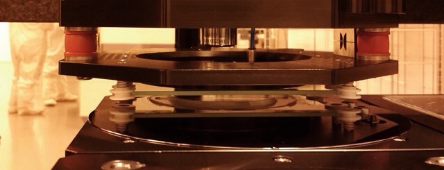 X-Celeprint's micro transfer printing technology. Source: X-Celeprint
- X-Celeprint has a printing process that places individual 'chiplets' of III-V material onto silicon
- The micro transfer printing technique can be used to make silicon photonics circuits
- X-Celeprint will work with silicon photonics companies interested in licensing its technology
A key challenge facing silicon photonics players is creating a light source. Silicon does not lase so a III-V material is needed to form the laser.
One approach is to attach a tiny module holding the laser to the silicon photonics design. This is what the likes of Cisco Systems, Luxtera, Mellanox Technologies and IBM are doing: adding an external laser to the otherwise monolithic silicon photonics circuit.
An alternative technique is to bond the III-V material to the silicon and using photolithography and etching to construct the silicon photonics device. The attraction of III-V bonding is that the technique can be used to also make the modulators and photo-detectors. Known as heterogeneous integration, this approach is being used by companies such as Aurrion, Intel and Skorpios Technologies.
"Bonding is an elegant solution," says Roel Baets, a professor at the Photonics Research Group at Ghent University. "You can make the light source at the wafer scale and have a single chip solution that looks like a monolithic chip, including the light source."
Think of printing as pick-and-place in a massively parallel fashion. Instead of ink, we are picking up and printing arrays of high-performance semiconductors.
Bonding III-V material to silicon is itself non-trivial. First, silicon wafers are either 200mm or 300mm (8 or 12 inch) while III-V indium phosphide wafers are typically 50mm (2 inch). Indium phosphide wafers are also expensive, simply etching away the majority of the wafer to leave small islands of wanted material is hugely wasteful.
"There is only going to be a laser here or there, with a fill factor - an area coverage - of some one percent," says Baets. "You are throwing away a lot of III-V."
Equally, cutting up the III-V wafer into small slivers for bonding is complicated as it requires precision placement; a process difficult to automate to achieve high-yield circuits. This is the challenge the heterogeneous integration companies have set themselves.
It is a market opportunity identified by start-up X-Celeprint. It has a process that places individual 'chiplets' of III-V material onto silicon by the thousands.
X-Celeprint uses a micro transfer printing to place the chiplets onto silicon. "Think of printing as pick-and-place in a massively parallel fashion," says Kyle Benkendorfer, CEO of X-Celeprint. "Instead of ink, we are picking up and printing arrays of high-performance semiconductors."
Micro transfer printing is already used commercially to make high concentration solar cells, and it is being evaluated to place thin lasers on read/ write heads in disc drives. "We can print live devices or a slab of material on any substrate as long as it is flat," says Benkendorfer.
One benefit of the technique is that the thin III-V material is removed from the indium phosphide wafer but the underlying substrate is retained and can be recycled. For wafer-to-wafer bonding, in contrast, the substrate must be ground back. "This is several hundred microns of [substrate] material," says Benkendorfer. "With our process you can reprocess the wafer and regrow it, saving some $3,000."
The printing process also lends itself to automation. "We can very efficiently place active die of highly expensive compound material at the point of use, where it can then be converted into a device," he says.
X-Celeprint wants to work with silicon photonics companies interested in licensing its printing technology. Developing the process with a particular silicon photonics vendor takes time. Each application requires tailoring and it can take up to two years to make, test and scale up production, says the start-up.
"We recognise that silicon photonics as a large market is out there, no question," says Benkendorfer. "But the development time to get any significant market is going to be a while."
Xtera demonstrates 40 Terabit using Raman amplification
- Xtera's Raman amplification boosts capacity and reach
- 40 Terabit optical transmission over 1,500km in Verizon trial
- 64 Terabit over 1,500km in 2015 using a Raman module operating over 100nm of spectrum
 Herve Fevrier
System vendor Xtera is using all these techniques as part of its Nu-Wave Optima system but also uses Raman amplification to extend capacity and reach.
"We offer capacity and reach using a technology - Raman amplification - that we have been pioneering and working on for 15 years," says Herve Fevrier, executive vice president and chief strategy officer at Xtera.
 The distributed amplification profile of Raman (blue) compared to an EDFA's point amplification. Source: Xtera
One way vendors are improving the amplification for 100 Gigabit and greater deployments is to use a hybrid EDFA/ Raman design. This benefits the amplifier's power efficiency and the overall transmission reach but the spectrum width is still dictated by Erbium to around 35nm. "And Raman only helps you have spans which are a bit longer," says Fevrier.
Meanwhile, Xtera is working on programable cards that will support the various transmission options. Xtera will offer a 100nm amplifier module this year that extends its system capacity to 24 Terabit (240, 100 Gig channels). Also planned this year is super-channel PM-QPSK implementation that will extend transmissions to 32 Terabit using the 100nm amplifier module. In 2015 Xtera will offer PM-16-QAM that will deliver the 48 Terabit over 2,000km and the 64 Terabit over 1,500km.
For Part 1, click here
MultiPhy eyeing 400 Gig after completing funding round
MultiPhy is developing a next-generation chip design to support 100 and 400 Gigabit direct-detection optical transmission. The start-up raised a new round of funding in 2013 but has neither disclosed the amount raised nor the backers except to say it includes venture capitalists and a 'strategic investor'.
The start-up is already selling its 100 Gig multiplexer and receiver chips to system vendors and module makers. The devices are being used for up to 80km point-to-point links and dense WDM metro/ regional networks spanning hundreds of kilometers. "In every engagement we have, the solutions are being sold in both data centre and telecom environments," says Avi Shabtai, CEO of MultiPhy.
The industry has settled on coherent technology for long-distance 100 Gig optical transmission but coherent is not necessarily a best fit for certain markets if such factors as power consumption, cost and compatibility with existing 10 Gig links are considered, says Shabtai.
The requirement to connect geographically-dispersed data centres has created a market for 100 Gig direct-detection technology. The types of data centre players include content service providers, financial institution such as banks, and large enterprises that may operate their own networks.
In every engagement we have, the solutions are being sold in both data centre and telecom environments
MultiPhy's two chips are the MP1101Q, a 4x25 Gig multiplexer device, and the MP1100Q four-channel receiver IC that includes a digital signal processor implementing the MLSE algorithm.
The chipset enables 10 Gig opto-electronics to be used to implement the 25 Gig transmitter and receiver channels. This results in a cost advantage compared to other 4x25 Gig designs. A design using the chipset can achieve 100 Gig transmissions over a 200GHz-wide channel or a more spectrally efficient 100GHz one. The latter achieves a transmission capacity of 4 Terabits over a fibre.
ADVA Optical Networking is one system vendor offering 100 Gig direct-detection technology while Finisar and Oplink Communications are making 100 Gigabit direct-detection optical modules. Oplink announced that it is using MultiPhy's chipset in 2013.
Overall, at least four system vendors are in advanced stages of developing 100 Gig direct-detection, and not all will necessarily announce their designs, says Shabtai. Whereas all the main optical transmission vendors have 100 Gig coherent technology, those backing 100 Gig direct detection may remain silent so as not to tip off their competitors, he says.
We assume we can do more using those [25 Gig] optical components with our technology
Meanwhile, the company is using the latest round of funding to develop its next-generation design. MultiPhy is focussed on high-speed direct-detection despite having coherent technology in-house. "Coherent is on our roadmap but direct detection is a very good opportunity over the next two years," says Shabtai. "You will see us come with solutions that also support 400 Gig."
A 400 Gigabit direct-detection design using its next generation chipset will likely come to market only in 2016 at the earliest by which time 25 Gig components will be more mature and cheaper. Using existing 25 Gig technology, a 400 Gig design requires 16, 25 Gig channels. However, the company will likely extend the performance of 25 Gig components to achieve even faster channel speeds, just like it does now with 10 Gig components to achieve 25 Gig speeds. The result will be a 400 Gig design with fewer than 16 channels. "We assume we can do more using those [25 Gig] optical components with our technology," says Shabtai.
Intel on silicon photonics and its role in the data centre

In the next couple of years, you will see a massive adoption of silicon photonics into the data centers and into high-performance computing
Mario Paniccia, Intel
Bringing new technology to market is at least a decade-long undertaking. So says Mario Paniccia, Intel Fellow and general manager of the company's silicon photonics operation. “The first transistor, the first chip; it has been 10 or 15 years from the first idea or research result to a commercial product,” he says. “Silicon photonics is just another example.”
Paniccia should know. He has been at Intel for nearly 20 years and started the company’s investigation of silicon photonics. Paniccia has overseen each of Intel’s various silicon photonics' building-block developments, beginning with a 1 Gigabit silicon modulator in 2004 through to its high gain-bandwidth avalanche photo-detector detailed in 2008.
Now Intel has unveiled its first 100 Gigabit silicon photonic product used as part of its Rack Scale Architecture (RSA) that implements a disaggregated system design that separates storage, computing and networking. The 100 Gigabit modules are used along with Terabit connectors and Corning's ClearCurve multi-mode fibre.
"Silicon photonics is the path to low-cost, high-volume optical connectivity in and around the server platform and in the data centre,” says Paniccia. “We can see it now coming.”
We are operating with a mindset of CMOS compatibility and we are putting our process and our photonics into fabs that also run high volume CMOS manufacturing
A key advantage of silicon photonics is its ability to benefit from high-volume manufacturing developed for the chip industry. But high-volume manufacturing raises its own challenges, such as determining where silicon photonics has value and picking the right applications.
Another merit, which at first does not sound like one, is that silicon photonics is 'good enough'. “But that 'good enough' is getting better and getting very close to performance levels of most of the modulation and detection devices people have shown in excess of 40 Gig," says Paniccia.
Such silicon-photonic building blocks can be integrated to deliver aggregate bandwidths of 100 Gig, 400 Gig, even a Terabit-per-second. “As demands increase in the data centre, cloud and high-performance computing, the ability to integrate photonics devices with CPUs or ASICs to deliver solutions at an architecture level, that is the really exciting part," says Paniccia.
At the end of the day, it is about building a technology that is cost effective for the application
Manufacturing process
Intel has not said what process it uses for its silicon photonic devices, although it does say it uses more than one. IBM uses 90nm lithography and STMicroelectronics has chosen 65nm for their silicon photonic designs.
Intel makes its photonics and associated drive electronics on separated devices due to the economics. Not using a leading manufacturing process for the photonics is cheaper since it avoids having to use expensive die and associated masks. “At the end of the day, it is about building a technology that is cost effective for the application," says Paniccia.
Intel uses a 22nm CMOS process and is moving to 14nm for its CPUs. For light, the feature sizes in silicon are far broader. “However, better lithography gets you better resolution, gets you better sidewalls roughness and better accuracy,” says Paniccia. “[A] 90nm [lithography] is plenty for most of the process nodes.”
Intel says it uses more advanced lithography for the early manufacturing steps of its silicon photonics devices, while the ’backend’ processing for its hybrid (silicon/ indium phosphide) laser involved broad metal lines and etch steps for which 130nm lithography is used.
The silicon photonics process is designed to be CMOS compatible so that the photonics can be made alongside Intel's volume chips. “That is critical,” says Paniccia. “We are operating with a mindset of CMOS compatibility and we are putting our process and our photonics into fabs that also run high volume CMOS manufacturing." The goal is to ensure that as production ramps, Intel can move its technology across plants.
The company has no plans to offer silicon photonics manufacturing as a foundry business.
Data centre trends
Intel is focussing its silicon photonics on the data centre. “We announced the RSA, a rack connected with switching, with silicon photonics and the new MXC cable,” says Paniccia. “Bringing optics up and down the racks and across racks, not only are the volumes quite big but the price points are aggressive.”
The company is using multi-mode fibre for its silicon photonics solution despite growing interest in single-mode fibre to meet the longer reach requirements emerging in the data centre.
Intel chose multi-mode as it results in a more economic solution in terms of packaging, assembly and cabling. "If you look at a single-mode fibre solution - coupling the fibre, packaging and assembling - it is very expensive," he says. That is because single-mode fibre requires precise fibre alignment at the module and at the connector, he says: "Even if the photonics were free, packaging, testing and assembly accounts for 40-60 percent of cost."
Silicon photonics is inherently single-mode and making it work with multi-mode fibre is a challenge. “At the transmitter side it is somewhat easy, a small hose - the transmitter - going into a big hose, a 50-micron [multi-mode] fibre, so the alignment is easy,“ says Paniccia. “At the receiver side, I now have a 50-micron multi-mode fibre and couple it down into a silicon photonic chip; that is the hard part.”
Corning's ClearCurve multi-mode fibre and the MXC connector working with Intel's 100 Gigabit modules achieve a 300m reach, while 820m has been demonstrated. “At the end of the day, the customer will decide how do we drive a new architecture into the next-generation of data centre,” says Paniccia.
Optics edge closer
Optics will edge up to chips as silicon photonics evolves. With electrical signals moving from 10 Gigabit to 25 Gigabit, it becomes harder to send the signals off chip. Embedding the optics onto the board, as Intel has done with its RSA, means that the electrical signal paths are only a couple of inches long. The signals are then carried optically via the MXC connector that supports up to 64 fibres. "Optical modules are limited in space and power," says Paniccia. "You have got to move to an embedded solution which enables greater faceplate density."
The next development after embedded modules will be to co-package the optics with the ASIC or CPU. "That is the RSA," says Paniccia. "That is the evolution that will have to happen when data rates run from 25 Gig to 32 Gig and 40 Gig line rates."
Moreover, once optics are co-packaged with an ASIC or a CPU, systems will be designed differently and optimised further, says Paniccia. "We have an Intel roadmap that takes it from a core technology for networking all the way to how we attach this stuff to CPUs," he says. "That is the end game."
Intel views silicon photonics not as a link technology but a connectivity approach for an architecture and platforms that will allow customers to evolve as their cloud computing and storage requirements grow.
"In the next couple of years, you will see a massive adoption of silicon photonics into the data centers and into high-performance computing, where the cost of I/O [input/output] has been limiting system development and system architecture," says Paniccia.
MACOM acquires Mindspeed to boost 100 Gig offerings
 Ray MoroneyThe Mindspeed acquisition increases the serviceable addressible market for MACOM, both geographical - the company will strengthen its presence in Asia Pacific - and by gaining new equipment vendor accounts. It also broadens MACOM's 100 Gigabit physical device portfolio.
"We are targeting the 100 Gig buildout and the growth coming from that," says Ray Moroney, product line manager, opto-device business unit at MACOM.
Mindpeed also makes a broad portfolio of crosspoint switches used in datacom equipment, and several families of communications processors.
With the acquisition of Mindspeed we have the full electronics bill-of-materials for CFP2 and CFP4 [module] client-side applications
MACOM entered opto-electronics with the acquisition of Optimai in 2011 that had long-haul and client-side modulator drivers and trans-impedance amplifiers (TIAs). Now with Mindspeed's products, MACOM can capture client-side designs with clock data recovery chips and quad-channel TIAs for 100 Gig modules. "With the acquisition of Mindspeed we have the full electronics bill-of-materials for CFP2 and CFP4 [module] client-side applications," says Moroney.
MACOM also gains silicon germanium technology alongside its indium phosphide and gallium arsenide technologies. Silicon germanium has a lower cost structure once a design is being made in volume production, says Moroney, but the R&D and mask costs are generally higher. Silicon germanium also allows significant integration. "It is BiCMOS in nature," says Moroney. "You can integrate full CMOS functionality into a design too." For example digital control can be added alongside analogue functions. Moroney says the company will use silicon germanium for high-performance analogue designs like TIAs as well as high-frequency millimeter wave and microwave applications.
The company is considering its options regarding the future of the communications processors arm of Mindspeed's business. "MACOM is very much an analogue/ RF company," says Moroney. "It [communications processors] is certainly not seen as a core area of investment for MACOM."
Books in 2013 - Part 2
Steve Alexander, CTO of Ciena
David and Goliath: Underdogs, Misfits, and the Art of Battling Giants by Malcolm Gladwell.
I’ve enjoyed some of Gladwell’s earlier works such as The Tipping Point and Outliers: The Story of Success. You often have to read his material with a bit of a skeptic's eye since he usually deals with people and events that are at least a standard deviation or two away from whatever is usually termed “normal.” In this case he makes the point that overcoming an adversity (and it can be in many forms) is helpful in achieving extraordinary results. It also reminded me of the many people who were skeptical about Ciena’s initial prospects back in the middle '90s when we first came to market as a “David” in a land of giant competitors. We clearly managed to prosper and have now outlived some of the giants of the day.
Overconnected: The Promise and Threat of the Internet by William Davidow.
I downloaded this to my iPad a while back and finally got to read it on a flight back from South America. On my trip what had I been discussing with customers? Improving network connections of course. I enjoyed it quite a bit because I see some of his observations within my own family. The desire to “connect” whenever something happens and the “positive feedback” that can result from an over-rich set of connections can be both quite amusing as well as a little scary! I don’t believe that all of the events that the author attributes to being overconnected are really as cause-and-effect driven as he may portray, but I found the possibilities for fads, market bubbles, and market collapses entertaining.
For another insight into such extremes see Extraordinary Popular Delusions and the Madness of Crowds by Charles Mackay, first published in the 1840s. We, as a species, have been a bit wacky for a long time.
Shadow Divers: The True Adventure of Two Americans Who Risked Everything to Solve One of the Last Mysteries of World War II by Robert Kurson.
Having grown up in the New York / New Jersey area and having listened to stories from my parents about the fear of sabotage in World War II (Google Operation Pastorius for some background) and grandparents, who had experienced the Black Tom Explosion during WW1, this book was a “don’t put it down till done” for me. I found it by accident when browsing a used book store. It’s available on Kindle and is apparently somewhat controversial because another diver has written a rebuttal to at least some of what was described. It is a great example of what it takes to both dive deep and solve a mystery.
David Welch, President, Infinera
Here is my cut. The first three books offer a perspective on how people think and I apply it to business.
- The Talent Code: Greatness Isn't Born. It's Grown. Here's How by Daniel Coyle.
- Mindset: The New Psychology of Success by Carol Dweck
- Moneyball: The Art of Winning an Unfair Game by Michael Lewis.
My non-work related book is Unbroken: A World War II Story of Survival, Resilience, and Redemption by Laura Hillenbrand.
Unfortunately, I rarely get time to read books, so the picking can be thin at times.
Marcus Weldon, President of Bell Labs and CTO, Alcatel-Lucent
I am currently re-reading Jon Gertner's history of Bell labs, called The Idea Factory: Bell Labs and the Great Age of American Innovation which should be no surprise as I have just inherited the leadership of this phenomenal place, and much of what he observes is still highly relevant today and will inform the future that I am planning.
I joined Bell Labs in 1995 as a post-doctoral researcher in the famous, Nobel-prize winning Physics Division (Div111, as it was known) and so experienced much of this first hand. In particular, I recall being surrounded by the most brilliant, opinionated, odd, inspired, collaborative, competitive, driven, relaxed, set of people I had ever met. And with the shared goal of solving the biggest problems in information and telecommunications.
Having recently returned back to the 'bosom of bell', I find that, remarkably, much of that environment and pool of talent still remains. And that is hugely exciting as it means that we still have the raw ingredients for the next great era of Bell Labs. My hope is that 10 years from now Gertner will write a second edition or updated version of the tale that includes the renewed success of Bell Labs, and not just the historical successes.
On the personal front, I am reading whatever my kids ask me to read them. Two of the current favourites are: Turkey Claus, about a turkey trying to avoid becoming the centrepiece of a Christmas feast by adapting and trying various guises, and Pete the Cat Saves Christmas, about a world of an ailing feline Claus, requiring average cat, Pete, to save the big day.
I am not sure there is a big message here, but perhaps it is that 'any one of us can be called to perform great acts, and can achieve them, and that adaptability is key to success'. And of course, there is some connection in this to the Bell Labs story above, so I will leave it there!
Books in 2013: Part 1, click here
First silicon photonics devices from STMicro in 2014
STMicroelectronics expects to have first silicon photonics products by mid-2014. The chip company announced the licensing of silicon photonics technology from Luxtera in March 2012. Since then STMicro has been developing its 300mm (12-inch) CMOS wafer manufacturing line for silicon photonics at its fab at Crolles, France.
 Flavio Benetti, STMicroelectronics
"We think we are the only ones doing the processing in a 12-inch line," says Flavio Benetti, general manager of mixed processes division at STMicroelectronics.
The company has a manufacturing agreement with Luxtera and the two continue to collaborate. "We have all the seeds to have a long-term collaboration," says Benetti.
"We also have the freedom to develop our own products." STMicro has long supplied CMOS and BiCMOS ICs to optical module makers, and will make the ICs and its photonic circuits separately.
The company's interest in silicon photonics is due to the growth in data rates and the need of its customers to have more advanced solutions at 100 Gig and 400 Gig in future.
"It is evident that traditional electronics circuits for that are showing their limits in terms of speed, reach and power consumption," says Benetti. "So we have been doing our due diligence in the market, and silicon photonics is one of the possible solutions."
It is evident that traditional electronics circuits for that are showing their limits in terms of speed, reach and power consumption
The chip company will need to fill its 300mm production line and is eyeing short-reach interconnect used in the data centre. STMicro is open to the idea of offering a foundry service to other companies in future but this is not its current strategy, says Benetti: "A foundry model is not excluded in the long term - business is business - but we are not going to release the technology to the open market as a wafer foundry."
The photonic circuits will be made using a 65nm lithography line, chosen as it offers a good tradeoff between manufacturing cost and device feature precision. Test wafers have already been run through the manufacturing line. "Being the first time we put an optical process in a CMOS line, we are very satisfied with the progress," says Benetti.
One challenge with silicon photonics is the ability to get the light in and out of the circuit. "There you have some elements like the gratings couplers - the shape of the grating couplers and the degree of precision are fundamental for the efficiency of the light coupling," says Benetti. "If you use a 90nm CMOS process, it may cost less but 65nm is a good compromise between cost and technical performance." The resulting photonic device and the electronics IC are bonded in a 3D structure and are interfaced using copper pillars.
A foundry model is not excluded in the long term - business is business - but we are not going to release the technology to the open market as a wafer foundry
Making the electronics and photonic chips separately has performance benefits and is more economical: the dedicated photonic circuit is optimised for photonics and there are fewer masks or extra processing layers compared to making an electro-optic, monolithic chip. The customer also has more freedom in the choice of the companion chip - whether to use a CMOS or BiCMOS process. Also some STMicro customers already have a electronic IC that they can reuse. Lastly, says Benetti, customers can upgrade the electronics IC without touching the photonic circuit.
Benetti is already seeing interest from equipment makers to use such silicon photonics designs directly, bypassing the optical module makers. Will such a development simplify the traditional optical supply chain? "There is truth in that; we see that," says Benetti. But he is wary of predicting disruptive change to the traditional supply chain. "System vendors understand the issue of the supply chain with the added margins [at each production stage] but to simplify that, I'm not so sure it is an easy job," he says.
Benetti also highlights the progress being made with silicon photonics circuit design tools.
STMicro's test circuits currently in the fab have been developed using electronic design automation (EDA) tools. "Already the first generation design kit is rather complete - not only the physical design tools for the optics and electronics but also the ability to simulate the system [the two together] with the EDA tools," says Benetti.
But challenges remain.
One is the ability to get light in and out of the chip in an industrial way. "Coupling the light in the fibre attachment - these are processes that still have a high degree of improvement," says Benetti. "The process of the fibre attachment and the packaging is something we are working a lot on. We have today at a very good stage of speed and precision in the placement of the fibres but there is still much we can do."
Compass-EOS raises $42M
Compass-EOS has raised $42 million in investment. The Israeli start-up launched its r10004 IP core router in March and has so far announced two customers: NTT Communications and the China Education and Research Network, CERNET. The company says it has a second, tier-one operator that has yet to be announced.
 Asaf Somekh with the icPhotonics chip
"Both global operators have purchased routers on several occasions for several types of deployments," says Asaf Somekh, vice president of marketing at Compass-EOS. “There are also a couple of smaller operators that we cannot disclose at this stage." The company is involved in several trials in the US, Japan and EMEA.
The r10004 core router uses the company's novel icPhotonics chip that has a Terabit-plus optical interface. The chip, which houses a merchant network processor, integrates 168, 8 Gigabit VCSELs and 168 photodetectors for a total bandwidth of 1.344Tbps in each direction.
Eight chips are connected in a full mesh, removing the need for a router's switch fabric and mid-plane that connect the router cards. The result is a 6U-sized compact router platform that saves on power and cost.
First router deployments have been operational for over a year. Somekh says customers have been positive about the router's ease of deployment, operation and robustness, and have not encountered significant issues with deployments. "This is very different from their past experiences of introducing a new vendor into their networks," he says.
The latest funding will be used to develop further the icPhotonics chip
Somekh also says that using the router delivers revenue benefits. Replacing a traditional three-chassis - 126U in total - core router with the 6U one has enabled the operator to deploy servers in the resulting reclaimed space. Deploying the router with servers in colocation data centres has turned them from cost centres into revenue-generating ones.
The company said the latest raised funding will be used to develop further the icPhotonics chip. Compass-EOS has talked about a future chip with channels operating at 32Gbps. “We're also investing in innovative software and on the marketing side, focussing on the US market and Japan with a stronger presence there,” says Somekh.
The company also announced it has cut staff. There are now 100 people working at the company compared to 150 employed in March. "Looking at the strategy moving forward we decided to make these adjustments to better fit the objectives and financial plan," says Somekh.
The latest round of investment takes the total amount of funding raised by the start-up to over $162 million. Investors in the latest round include Comcast Ventures and Cisco Systems.