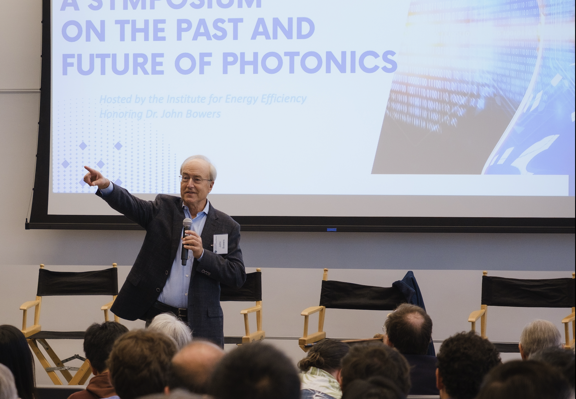
John Bowers: We are still at the dawn of photonics
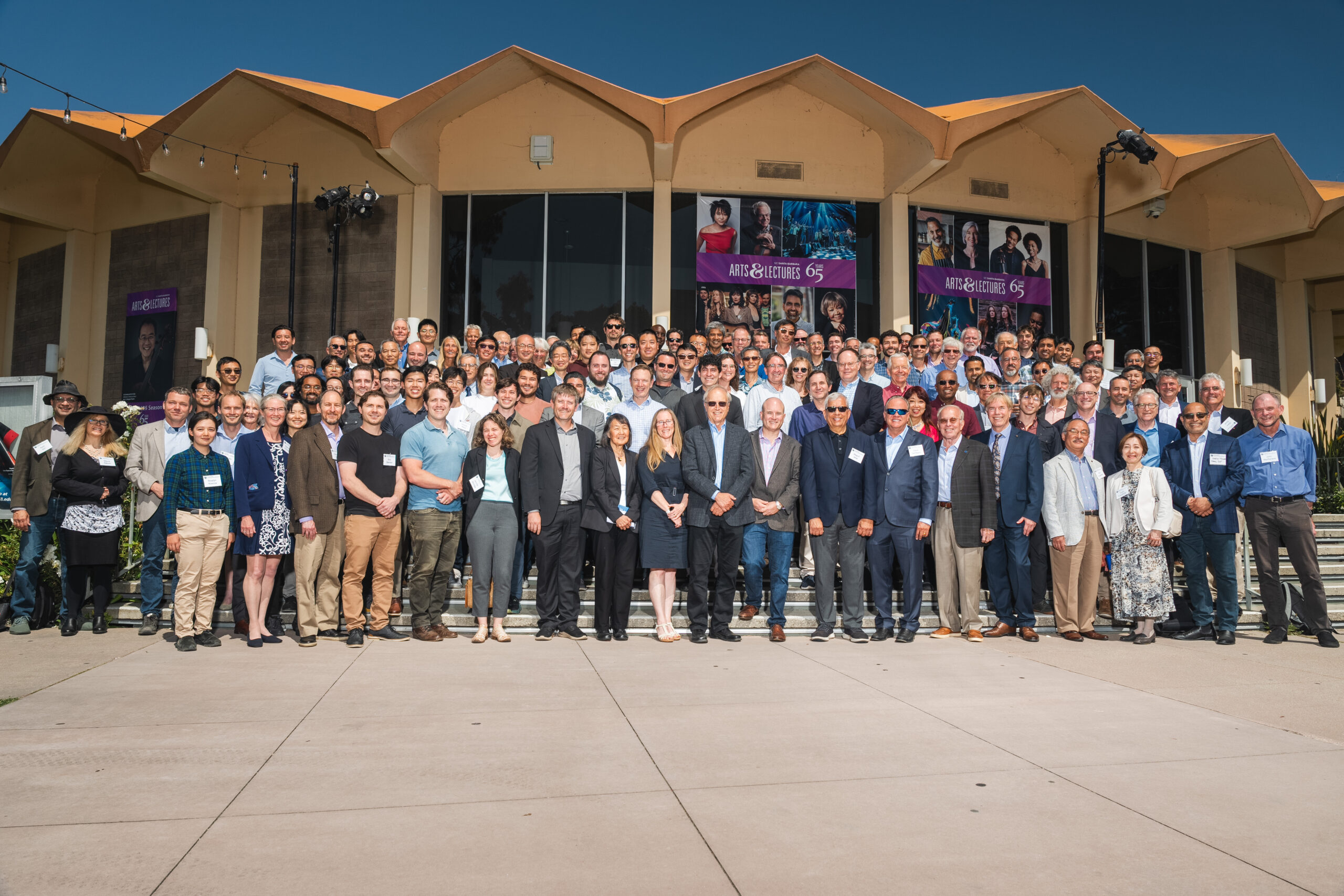
After 38 years at the University of California, Santa Barbara (UCSB), Professor John Bowers (pictured) is stepping away from teaching and administrative roles to focus on research.
He welcomes the time it will free for biking and golf. He will also be able to linger, not rush, when travelling. On a recent trip to Saudi Arabia, what would have centered around a day-event became a week-long visit.
Bowers’ career includes significant contributions to laser integration and silicon photonics, mentoring some 85 PhD students, and helping found six start-ups, two of which he was the CEO.
Early Influences
Bowers’ interest in science took root while at high school. He built oscilloscopes and power supplies using Heathkits, then popular educational assemblies for electronics enthusiasts. He was also inspired by his physics and chemistry teachers, subjects he majored in at the University of Minnesota.
A challenging experience led him to focus solely on physics: “I took organic chemistry and hated it,” says Bowers. “I went, ‘Okay, let’s stick to inorganic materials.’”
Bowers became drawn to high-energy physics and worked in a group conducting experiments at Fermilab and Argonne National Laboratories. Late-night shifts – 10 PM to 6 AM – offered hands-on learning, but a turning point came when his mentor was denied tenure. “My white knight fell off his horse,” he says.
He switched to applied physics at Stanford, where he explored gallium arsenide and silicon acoustic devices, working under the supervision of the late Gordon Kino, a leading figure in applied physics and electrical engineering.
Bowers then switched to fibre optics, working in a group that was an early leader in single-mode optical fibre. “It was a period when fibre optics was just taking off,” says Bowers. “In 1978, they did the first 50-megabit transmission system, and OFC [the premier optical fibre conference] was just starting.”
Bell Labs and fibre optics
After gaining his doctorate, Bowers joined Bell Labs, where his work focused on the devices—high-speed lasers and photodetectors—used for fibre transmission. He was part of a team that scaled fibre-optic systems from 2 to 16 gigabits per second. However, the 1984 AT&T breakup signalled funding challenges, with Bell Labs losing two-thirds of its financial support.
Seeking a more stable environment, Bowers joined UCSB in 1987. He was attracted by its expertise in semiconductors and lasers, including the presence of the late Herbert Kroemer, who went on to win the 2000 Nobel Prize in Physics. Kroemer developed the double heterostructure laser and played a big part in enticing Bowers to join. Bowers was tasked with continuing the laser work, something he has done for the last 40 years.
“Coming to Santa Barbara was brilliant, in retrospect,” says Bowers, citing its strong collaborative culture and a then newly formed materials department.
Integrated lasers
At UCSB, Bowers worked on integrated circuits using indium phosphide, including tunable lasers and 3D stacking of photonic devices.
At the same time, the field of silicon photonics was starting after Richard Soref wrote a seminal paper proposing silicon as an optical material for photonic integrated circuits (PIC).
“We all knew that silicon was a terrible light emitter because it is an indirect band-gap material,” says Bowers. “So when people started talking about silicon photonics, I kept thinking: ‘Well, that is fine, but you need a light source, and if you don’t have a light source, it’ll never become important.’”
Bowers tackled integrating lasers onto silicon to address the critical need for an on-chip light source. He partnered with Intel’s Mario Paniccia and his team, which had made tremendous progress developing a silicon Raman lasers with higher powers and narrower linewidths.
“It was very exciting, but you still needed a pump laser; a Raman laser is just a wavelength converter from one wavelength to another,” says Bowers. “So I focused on the pump laser end, and the collaboration benefitted us both.”
Intel commercialised the resulting integrated laser design and sold millions of silicon-photonics-based pluggable transceivers.
“Our original vision was verified: the idea that if you have CMOS processing, the yields will be better, the performance will be better, the cost will be lower, and it scales a lot better,” says Bowers. “All that has proven to be true.
Is Bowers surprised that integrated laser designs are not more widespread?
All the big silicon photonics companies, including foundry TSMC, will incorporate lasers into their products, he says, just as Intel has done and Infinera before that.
Infinera, an indium phosphide photonic integrated circuit (PIC) company now acquired by Nokia, claimed that integration would improve the reliability and lower the cost, says Bowers: “Infinera did prove that with indium phosphide and Intel did the same thing for silicon.”
The indium phosphide transceiver has a typical failure rate of 10 FIT (failures per ten billion hours), and if there are 10 laser devices, the FIT rises to 100, he says. By contrast, Intel’s design has a FIT of 0.1, and so with 10, the FIT becomes on the order of 1.
Silicon lasers are more reliable because there’s no III-V material exposed anywhere. Silicon or silicon dioxide facets eliminate the standard degradation mechanisms in III-V materials. This enables non-hermetic packaging, reducing costs and enabling rapid scaling.
According to Bowers, Intel scaled to a million transceivers in one year. Such rapid scaling to high volumes is important for many applications, and that is where silicon photonics has an advantage.
“Different things motivate different people. For me, it’s not about money, it’s more about your impact, particularly on students and research fields. To the extent that I’ve contributed to silicon photonics becoming important and dynamic, that is something I’m proud of.”
-Professor John Bowers
Optical device trends
Bowers notes how the rise of AI has surprised everyone, not just in terms of the number of accelerator chips needed but their input-output (I/O) requirements.
Copper has been the main transmission medium since the beginning of semiconductor chips, but that is now being displaced by optics – silicon photonics in particular – for the communications needs of very high bandwidth chips. He also cites companies like Broadcom and Nvidia shipping co-packaged optics (CPO) for their switching chips and platforms.
“Optics is the only economic way to proceed, you have to work on 3D stacking of chips coupled with modern packaging techniques,” he says, adding that the need for high yield and high reliability has been driving the work on III-V lasers on silicon.
One current research focus for Bowers is quantum dot lasers, which reduce the line width and minimise reflection sensitivity by 40dB. This eliminates the need for costly isolators in datacom transceivers.
Quantum dot devices also show exceptional durability, with lifetimes for epitaxial lasers on silicon a million times longer than quantum well devices on silicon and 10 times less sensitivity to radiation damage, as shown in a recent Sandia National Labs study for space applications.
Another area of interest is modulators for silicon photonics. Bowers says his group is working on sending data at 400 gigabits-per-wavelength using ‘slow light’ modulators. These optical devices modulate the intensity or phase, of light. Slowing down the light improves its interaction in the material, improving efficiency and reducing device size and capacitance. He sees such modulators is an important innovation.
“Those innovations will keep happening; we’re not limited in terms of speed by the modulator,” says Bowers, who also notes the progress in thin-film lithium niobate modulators, which he sees as benefiting silicon photonics, “We have written papers suggesting most of the devices may be III-V,” says Bowers, and the same applies to materials such as thin-film lithium niobate.
“I believe that as photonic systems become more complex, with more lasers and amplifiers, then everyone will be forced to integrate,” says Bowers.
Other applications
Beyond datacom, Bowers sees silicon photonics enabling LIDAR, medical sensors, and optical clocks. His work on low-noise lasers, coupled to silicon nitride waveguides, reduces phase noise by 60dB, enhancing sensor sensitivity. “If you can reduce the frequency noise by 60dB, then that makes it either 60dB more efficient, or you need 60dB less power,” he says.
Applications include frequency-based sensors for gas detection, rotation sensing, and navigation, where resonance frequency shifts detect environmental changes.
Other emerging applications include optical clocks for precise timing in navigation, replacing quartz oscillators. “You can now make very quiet clocks, and at some point we can integrate all the elements,” Bowers says, envisioning chip-scale solutions.
Mentorship and entrepreneurial contributions
Bowers’ impact extends to mentorship, guiding so many PhD students who have gone on to achieve great success.
“It’s very gratifying to see that progression from an incoming student who doesn’t know what an oscilloscope is to someone who’s running a group of 500 people,” he says.
Alan Liu, former student and now CEO of the quantum dot photonics start-up Quintessent, talks about how Bowers calls on his students to ‘change the world’.
Liu says it is not just about pushing the frontiers of science but also about having a tangible impact on society through technology and entrepreneurship.”
Bowers co-founded UCSB’s Technology Management Department and taught entrepreneurship for 30 years. Drawing on mentors like Milton Chang, he focused on common start-up pitfalls: “Most companies fail for the same set of reasons.”
His own CEO start-up experience informed his teaching, highlighting interdisciplinary skills and team dynamics.
Mario Paniccia, CEO of Anello Photonics, who collaborated with Bowers as part of the Intel integrated laser work, highlights Bowers’ entrepreneurial skills.
“John is one of the few professors who are not only brilliant and technically a world expert – in John’s case, in III-V materials – but also business savvy and entrepreneurial,” says Paniccia. “He is not afraid to take risks and can pick and hire the best.”
Photonics’ future roadmap
Bowers compares photonics’ trajectory to electronics in the 1970s, when competing CMOS technologies standardised, shifting designers’ focus from device development to complex circuits. “Just like in the 1970s, there were 10 competing transistor technologies; the same consolidation will happen in photonics,” he says.
Standardised photonic components will be integrated into process design kits (PDKs), redirecting research toward systems like sensors and optical clocks.
“We’re not at the end, we’re at the beginning of photonics,” emphasises Bowers.
Reflections
Looking back, would he have done anything differently?
A prolonged pause follows: “I’ve been very happy with the choices I have made,” says Bowers, grateful for his time at UCSB and his role in advancing silicon photonics.
Meanwhile, Bowers’ appetite for photonics remains unwavering: “The need for photonic communication, getting down to the chip level, is just going to keep exploding,” he says.

Mario Paniccia: We are just at the beginning
 During that time, his Intel team had six silicon photonics papers published in the science journals, Nature and Nature Photonics, and held several world records - for the fastest modulator, first at 1 gigabit, then 10 gigabit and finally 40 gigabit, the first pulsed and continuous-wave Raman silicon laser, the first hybrid silicon laser working with The University of California, Santa Barbara, and the fastest silicon germanium photo-detector operating at 40 gigabit.
It got to the stage where Intel’s press relations department would come and ask what the team would be announcing in the coming months. “ 'Hey guys,' I said, 'it doesn't work that way ' ”.
Since leaving Intel last year, Paniccia has been working as a consultant and strategic advisor. He is now exploring opportunities for silicon photonics but in segments other than telecom and datacom.
“I didn't want to go into developing transceivers for other big companies and compete with my team's decade-plus of development; I spent 20 years at Intel,” he says.
Decade of development
Intel’s silicon photonics work originated in the testing of its microprocessors using a technique known as laser voltage probing. Infra-red light is applied to the back side of the silicon to make real-time measurements of the chip’s switching transistors.
For Paniccia, it raised the question: if it is possible to read transistor switching using light, can communications between silicon devices also be done optically? And can it be done in parallel to the silicon rather than using the back side of silicon?
In early 2000 Intel started working with academic Graham Reed, then at the University of Surrey, and described by Paniccia as one of the world leaders in silicon photonics devices. “We started with simple waveguides and it just progressed from there,” he says.
The Intel team set the target of developing a silicon modulator working at 1 gigahertz (GHz); at the time, the fastest silicon modulator operated at 10 megahertz. “Sometimes leadership is about pushing things out and putting a stake in the ground,” he says.
It was Intel’s achievement of a working 1GHz silicon modulator that led to the first paper in Nature. And by the time the paper was published, Intel had the modulator working at 2GHz. The work then progressed to developing a 10 gigabit-per-second (Gbps) modulator and then broadened to include developing other silicon photonics building-block devices that would be needed alongside the modulator – the hybrid silicon laser, the photo-detector and other passive devices needed for an integrated transmitter.
There is a difference between proving the technology works and making a business out of it
Once 10Gbps was achieved, the next milestone was 20Gbps and then 40Gbps. Once the building block devices achieved operation in excess of 40Gbps, Intel’s work turned to using these optical building blocks in integrated designs. This was the focus of the work between 2010 to 2012. Intel chose to develop a four-channel 40Gbps (4x10 gigabit) transceiver using four-wavelength coarse WDM which ended up working at 50Gbps (4x12.5 gigabit) and then, most recently, a 100Gbps transceiver.
He says the same Intel team is no longer talking about 50Gbps or 100Gbps but how to get multiple terabits coming out of a chip.
Status
Paniccia points out that in little more than a decade, the industry has gone from not knowing whether silicon could be used to make basic optical functions such as modulators and photo-detectors, to getting them to work at speeds in excess of 40Gbps. “I’d argue that today the performance is close to what you can get in III-V [compound semiconductors],” he says.
He believes silicon photonics is the technology of the future, it is just a question of when and where it is going to be applied: “There is a difference between proving the technology works and making a business out of it”.
In his mind, these are the challenges facing the industry: proving silicon photonics can be a viable commercial technology and determining the right places to apply it.
For Paniccia, the 100-gigabit market is a key market for silicon photonics. “I do think that 100 gigabit is where the intercept starts, and then silicon photonics becomes more prevalent as you go to 200 gigabit, 400 gigabit and 1 terabit,” he says.
So has silicon photonics achieved its tipping point?
Paniccia defines the tipping point for silicon photonics as when people start believing the technology is viable and are willing to invest. He cites the American Institute for Manufacturing Integrated Photonics (AIM Photonics) venture, the $610 million public and private funded initiative set up in 2015 to advance silicon photonics-based manufacturing. Other examples include the silicon photonics prototyping service coordinated by nano-electronics research institute imec in Belgium, and global chip-maker STMicroelectronics becoming a silicon photonics player having developed a 12-inch wafer manufacturing line.
Instead of one autonomous LIDAR system in a car, you could have 20 or 50 or 100 sprinkled throughout your vehicle
“All these are places where people not only see silicon photonics as viable but are investing significant funds to commercialise the technology,” says Paniccia. “There are numerous companies now selling commercialised silicon photonics, so I think the tipping point has passed.”
Another indicator that the tipping point has happened, he argues, is that people are not spending their effort and their money solely on developing the technology but are using CMOS processes to develop integrated products.
“Now people can say, I can take this process and build integrated devices,” he says. “And when I put it next to a DSP, or an FPGA, or control electronics or a switching chip, I can do things that you couldn't do next to bulky electronics or bulky photonics.”
It is this combination of silicon photonics with electronics that promises greater computing power, performance and lower power consumption, he says, a view shared by another silicon photonics luminary, Rockley Photonics CEO, Andrew Rickman.
Moreover, the opportunities for integrated photonics are not confined to telecom and datacom. “Optical testing systems for spectroscopy today is a big table of stuff - lasers, detectors modulators and filters,” says Paniccia. Now all these functions can be integrated on a chip for such applications as gas sensing, and the integrated photonics device can then be coupled with a wireless chip for Internet of Things applications.
The story is similar with autonomous vehicle systems that use light detection and ranging (LIDAR) technology. “These systems are huge, complicated, have a high power consumption, and have lots of lasers that are spinning around,” he says. “Now you can integrate that on a chip with no moving parts, and instead of one autonomous LIDAR system in a car, you could have 20 or 50 or 100 sprinkled throughout your vehicle”
Disruptive technology
Paniccia is uncomfortable referring to silicon photonics as a disruptive technology. He believes disruption is a term that is used too often.
Silicon photonics is a technology that opens up a lot of new possibilities, he says, as well as a new cost structure and the ability to produce components in large volume. But it doesn’t solve every problem.
The focus of the optical vendors is very much on cost. For markets such as the large-scale data centre, it is all about achieving the required performance at the right cost for the right application. Packaging and testing still account for a significant part of the device's overall cost and that cannot be forgotten, he says.
Paniccia thus expects silicon photonics to co-exist with the established technologies of indium phosphide and VCSELs in the near term.
“It is all about practical decisions based on price, performance and good-enough solutions,” he says, adding that silicon photonics has the opportunity to be the mass market solution and change the way one thinks about where photonics can be applied.
“Remember we are just at the beginning and it will be very exciting to see what the future holds.”