
Avicena partners with TSMC to make its microLED links
TSMC, the leading semiconductor foundry, will make the photo-detectors used for Avicena Tech’s microLED optical interconnect technology.
Avicena is developing an optical interface that uses hundreds of parallel fibre links – each link comprising a tiny LED tranmitter and a silicon photo-detector receiver – to deliver terabit-per-second (Tbps) data transfers.
Avicena is targeting its microLED-based interconnect, dubbed LightBundle, for artifical intelligence (AI) and high-performance computing (HPC) applications.
The deal is a notable step for Avicena, aligning its technology with TSMC’s CMOS manufacturing prowess. The partnership will enable Avicena to transition its technology from in-house prototyping to high-volume production.
Visible-light technology
Avicena’s interconnects operate in the visible light spectrum at 425-430nm (blue light), differing from the near-infrared used by silicon photonics. The lower wavelength band enables simpler photo-detector designs where silicon efficiently absorbs blue light.
“Silicon is a very good detector material because the absorption length at that kind of wavelength is less than a micron,” says Christoph Pfistner, vice president of sales and marketing at Avicena. “You don’t need any complicated doping with germanium or other materials required for infrared detectors.”
Visible-light detectors can therefore be made using CMOS processes. For advanced CMOS nodes, however, such as used to make AI chips, hybrid bonding is required with a separate photo-detector wafer.
TSMC is adapting its CMOS Image Sensor (CIS) process used for digital cameras that operate in the megahertz range, to support Avicena’s photo-detectors that must work in the gigahertz range.
For the transmitter, Avicena uses gallium nitride-based microLEDs developed for the micro-display industry, paired with CMOS driver chips. Osram is Avicena’s volume LED supplier.
Osram has adapted its LED technology for high-speed communications and TSMC is now doing the same for the photo-detectors, enabling Avicena to mass produce its technology.
Specifications
The LED is used to transmit non-return-to-zero (NRZ) signalling at 3.5 to 4 gigabit-per-second (Gbps). Some 300 lanes are used to send the 800 gigabit data payload, clock, and associated overhead bits.
For the transmitter, a CMOS driver modulates the microLED while the receiver comprises a photo-detector, a trans-impedance amplifier (TIA) and a limiting amplifier.
By operating in this ‘slow and wide’ manner, the power consumption of less than 1 picojoule-per-bit (pJ/b) is achievable across 10m of the multi-mode fibre bundle. This compares to 3-5pJ/b using silicon photonics and up to 20pJ/b for optical pluggable transceivers though the latter support longer reaches.
The microLED links achieve a bandwidth density of over 1 terabit/mm and Avicena says this can be improved. Since the design is a 2D array, it is possible to extend the link density in area (in 2D) and not be confined to the ‘beachfront’ stretch. But this will be within certain limits, qualifies Pfistner
Applications
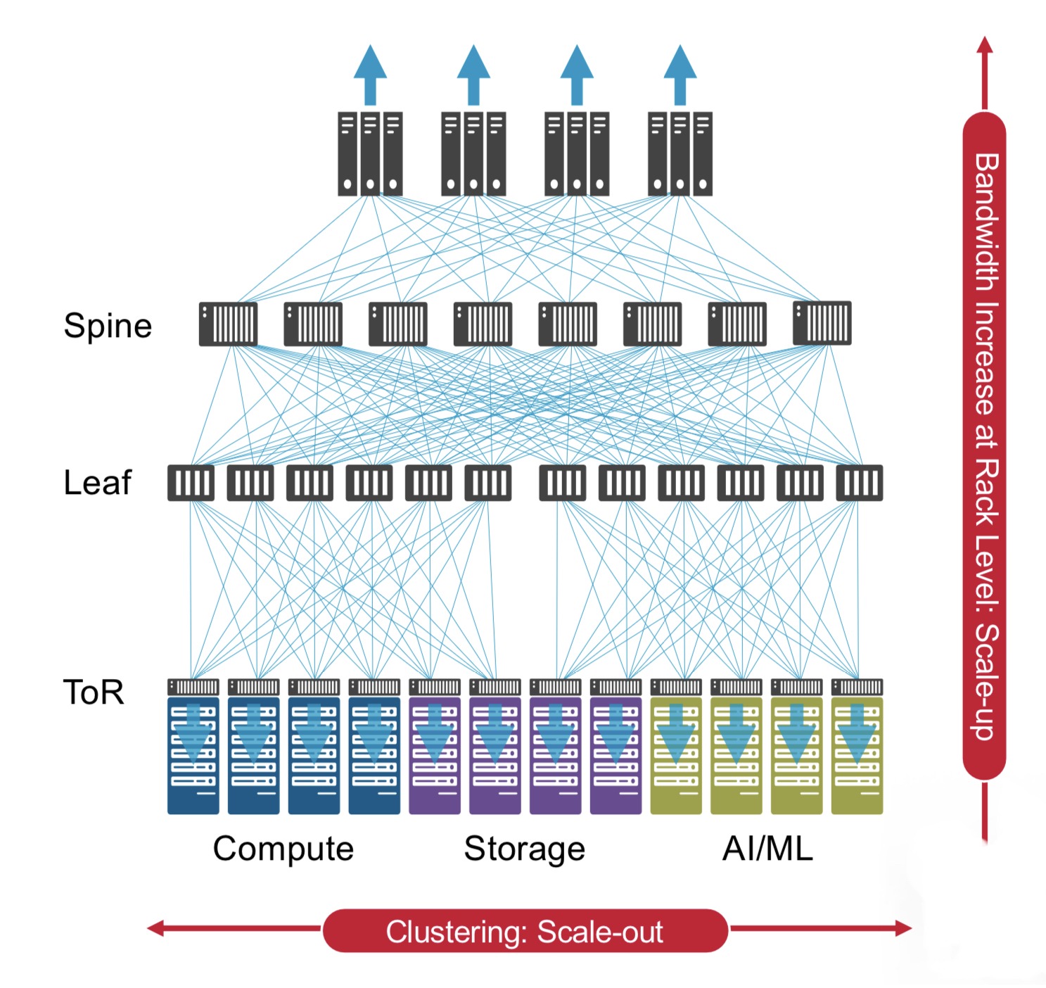
A key theme at the recent OFC 2025 show was optical interconnect options to linearly scale AI processing performance by adding more accelerator chips, referred to as the scale-up architecture.
At present copper links are used to scale up accelerators but the consensus is that, at some point, optics will be needed once the speed-distance performance of copper is exceeded. Nvidia’s roadmap suggests that copper can still support larger scale-up architectures for at least a couple of graphics processing unit (GPU) generations yet.
Avicena is first targeting its microLED technology in the form of an optical engine to address 1.6Tbps on-board optics modules. The same optical engine can also be used in active optical cables.
The company also plans to use its optical engine for co-packaged optics, and for in-package interconnect applications using a die-to-die (D2D) electrical interface such as the Universal Chiplet Interconnect Express (UCIe) or the OCP’s Bunch of Wires (BOW) interface. On-board optics, also known as co-packaged optics, refers to optics on a separate substrate close to the host ASIC, with both packaged together.
One such application for in-packaged optics is memory disaggregation involving high-bandwidth memory (HBM). “There’s definitely more and more interest in what some people refer to as optical HBM,” says Pfistner. He expects initial deployment of optical HBM in the 2029-2030 timeframe.
The foundry TSMC is also active in silicon photonics, developing the technology as part of its advanced system-in-package technology roadmap. While it is early days, Avicena’s microLED LightBundle technology could become part of TSMC’s optical offerings for applications such as die-to-die, xPU-to-memory, and in-packaged optics.
Nubis' bandwidth-packed tiny optical engine

- Nubis Communications has revealed its ambitions to be an optical input-output (I/O) solutions provider
- Its tiny 1.6-terabit optical engine measures 5mm x 7.5mm
- The optical engine has a power consumption of below 4 picojoule/bit (pJ/b) and a bandwidth density of 0.5 terabits per millimetre.
- “Future systems will be I/O with an ASIC dangling off it.”
Nubis Communications has ended its period of secrecy to unveil an optical engine targeted at systems with demanding data input-output requirements.
The start-up claims its optical engine delivers unmatched bandwidth density measured in terabits per millimetre (T/mm) and power consumption performance metrics.
“In the timeframe of founding the company [in 2020], it became obvious that the solution space [for our product] was machine learning-artificial intelligence,” says Dan Harding, the CEO of Nubis.
Company Background
Nubis has raised over $40 million, with the lead investor being Matrix Partners. Venture capital company Matrix Partners backed Acacia Communications, acquired by Cisco in 2021.
Other Nubis backers are Weili Dai, a co-founder of Marvell Technologies, and Belgium-based imec.xpand.

“We have raised enough money to get to production with our product,” says Harding, who joined Nubis in 2021 from Broadcom.
Peter Winzer is the CTO and founder of the company. Formerly at Nokia Bell Labs, Winzer was the 2018 winner of the Optica (then OSA) and IEEE Photonics Society’s John Tyndall Award for his work on coherent optical communications.
Nubis has 40 staff, mostly engineers.
“As a team, we are multidisciplinary,” says Winzer. The company’s expertise includes silicon photonics, analogue IC design including serialisers/ deserialisers (serdes), packaging – electrical and optical, and software including advanced simulation tools.
“It is all geared towards a systems solution,” says Winzer. “We are not just looking at the PIC [photonic integrated circuit] or the electronics; we have the system and the architecture in mind.”
The input-output challenge
Machine learning workloads continue to grow at a staggering pace, doubling more than twice each year. Not surprisingly, computing systems running such workloads are struggling to keep up.
Scaling such systems not only requires more processing – more graphics processing units (GPUs) – but also networking to connect clusters of GPUs.
What the compute vendors want is any-to-any connectivity between processors and between clusters. This is creating a tremendous input-output challenge in terms of bandwidth density while keeping the power consumption under control.
“Over half the power of that cluster can be taken up by traditional optics,” says Harding. “So it is clear that the industry wants new solutions.”
“Whatever cents-per-gigabit [figure] you use, if you multiply it by the I/O capacity, the number you’ll get is many times that of [the cost of] an ASIC,” adds Winzer. “We say that future systems will be I/O with an ASIC dangling off it.”

Design details
Nubis’ optical engine is a 16 x 112-gigabit design with a footprint of 5mm x 7.5mm.
“Because we have our electronics flip-chipped on top, that’s the entire footprint,” says Winzer. “We maintain that it is the highest density by far of any optical engine.”
Nubis says many parallel fibres can be interfaced to the optical engine despite its tiny size.
Supporting parallel fibres is essential for machine learning systems as the fibres are fanned out to enable any-to-any connectivity.
Nubis’ engine uses a 4 by DR4 fan-out architecture with 36 fibres arranged in a 3×12 array.
Surface coupling in a 2D array interfaces the 36 fibres to the PIC: 32 fibres are for data and four for the external laser light source.
There is only a physical limit to the number of fibres that can be connected if edge coupling is used, says Winzer. But surface coupling in a 2D array means the optical engine delivers 5-10x more density than its competitors.
The start-up also has designed the engine’s electronics: the optical modulator driver and the trans-impedance amplifier (TIA). The electronics use advanced equalisation to boost the electrical channel, given direct drive has demanding requirements, says Harding.
The XT1600 optical module
Nubis’ first product is the XT1600 optical module. Here, a substrate houses the company’s PIC and electronics onto which is packaged a lid containing the optical fibres.
Nubis has developed in-house the packaging and the fibre attach solution.
The substrate is 15x15mm, somewhat larger than the engine. Harding says this is deliberate to support products under development.
The 1.6 terabits – in fact, 16x112Gbps full duplex – module has a 2km reach. Its power consumption is below 4 pJ/b.
The fibres exit the module vertically and bend to the side. “[Going] vertical is good but the 2D is the much more important aspect here,” says Winzer.
A 2D approach is logical, says Nubis. An electrical ball grid array (BGA) all the bottom surface. It makes sense that the optics is similarly massively 2D, especially for designs where its a 100-gigabit electrical signal in and a 100-gigabit optical signal out.
Multiple rings of optical I/O engines can surround the ASIC because the fibres exit vertically. “Nobody else can do that because they are escaping from the [PIC] edge,” says Winzer.
Winzer highlights another benefit of the design.
The Universal Chiplet Interconnect Express (UCIe) specification calls for 2T/mm bandwidth escape density. An optical chiplet can only achieve this if wavelength-division multiplexing (WDM) is used due to the large fibre size. Nubis can achieve this density optically without having to use WDM because of 2D surface coupling.
Doing all-to-all at scale remains a big system challenge. “We’re just a part of that challenge,” says Harding. But for optical I/O to become pervasive in the data centre over the next five years, the optics must be significantly lower power, smaller, and efficient.
“If you crack that 2D nut, you can do many, many great things down the road,” says Winzer. “We’ve solved a huge technology problem that allows us to scale much better than anybody else.”
Status
Nubis has not named its foundry and contract manufacturing partners but says they are large, high-volume manufacturers.
Harding says there are now up to five credible silicon photonic foundries available.
“There was some early product definition which some foundries were better suited to support,“ says Harding. “And there was a robustness of the initial PDKs [process design kits] to get us an early product that was important to us.”
Choosing a contract manufacturer proved easier, given the maturity of the players.
Nubis’ first product has 16 optical channels each at 112 gigabit, but future designs will offer N by 224-gigabit channels.
Meanwhile, the XT1600 optical engine is available for sampling.

Tencent makes its co-packaged optics move

- Tencent is the first hyperscaler to announce it is deploying a co-packaged optics switch chip
- Tencent will use Broadcom’s Humboldt that combines its 25.6-terabit Tomahawk 4 switch chip with four optical engines, each 3.2 terabit-per-second (Tbps)
Part 2: Broadcom’s co-packaged optics
Tencent will use Broadcom’s Tomahawk 4 switch chip co-packaged with optics for its data centres.
“We are now partnered with the hyperscaler to deploy this in a network,” says Manish Mehta, vice president of marketing and operations optical systems division, Broadcom. “This is a huge step for co-packaged optics overall.”
Broadcom demonstrated a working version of a Humboldt switch at OFC earlier this year.
The Chinese hyperscaler will use Broadcom’s 25.6Tbps Tomahawk 4 Humboldt, a hybrid design where half of the chip’s input-output (I/O) is optical and half is the chip’s serialisers-deserialisers (serdes) that connect to pluggable modules on the switch’s front panel.
Four Broadcom 3.2-terabit silicon photonics-based optical engines are co-packaged alongside the Tomahawk 4 chip to implement 12.8Tbps of optical I/O.
Broadcom demonstrated a working version of a Humboldt switch at OFC earlier this year.
Co-packaged optics
Broadcom started its co-packaged optics development work in 2019.
“One of the reasons for our investment in co-packaged optics was that we did see firsthand the ongoing limits of copper interconnect being approached,” says Mehta.
The transmission reach of copper links continues to shrink as the signalling speed has increased from 25 gigabits-per-second (Gbps) non-return to zero (NRZ) to PAM-4 (4-level pulse amplitude modulation) based signalling at 56Gbps, 112Gbps and, in the coming years, 224Gbps. Power consumption is also rising with each speed hike.
Broadcom says data centres now use 1 million optical interconnects, but that much of the connectivity is still copper-based, linking adjacent racks and equipment within the rack.
“Hyperscalers spend ten times more on interconnects than switching silicon,” says Mehta. Given these trends, there needs to be a continual improvement in the power profile, cost and scaled manufacturing of optical interconnect, he says.
In the short term, what is driving interest in co-packaged optics is overcoming the limitations of copper, says Broadcom.
In early 2021, Broadcom detailed at a JP Morgan event its co-packaged optics roadmap. Outlined was the 25.6-terabit Humboldt to be followed by Bailly, a 51.2-terabit all co-packaged optics design using Broadcom’s Tomahawk 5 switch chip which is now sampling.
Humboldt uses DR4 (4×100-gigabit using 4 fibres) whereas the 51.2-terabit Bailly will add multiplexing-demultiplexing and use the FR4 specification (4×100-gigabit wavelengths per fibre).
Technology and partners
Broadcom’s in-house technology includes lasers (VCSELs and EMLs), mixed-signal expertise (trans-impedance amplifiers and drivers), and silicon photonics, as well as its switch chips.
Broadcom uses a remote laser source for its co-packaged optics design. Placing the laser away from the package (the switch chip and optics) means no cooling is needed.
Broadcom is working with 15 partners to enable its co-packaged optics, highlighting the breadth of expertise required and the design complexity.
There are two prominent use cases for the hybrid I/O Humboldt.
One is for top-of-rack switches, where the electrical interfaces support short-reach copper links connecting the servers in a rack, while the optical links connect the top-of-rack box to the next layer of aggregation switching.
The second use is at the aggregation layer, where the electrical I/O connects other switches in the rack while the optical links connect to switch layers above or below the aggregation layer.
“There is a use case for having pluggable ports where you can deploy low-cost direct-attached copper,” says Mehta.
Broadcom says each data centre operator will have their own experience with their manufacturing partners as they deploy co-packaged optics. Tencent has decided to enter the fray with 25.6-terabit switches.
“It is not just Broadcom developing the optical solution; it is also ensuring that our manufacturing partner is ready to scale,” says Mehta.
Ruijie Networks is making the two-rack-unit (2RU) switch platform for Tencent based on Broadcom’s co-packaged optics solution. The co-packaged optics interfaces are routed to 16 MPO connectors while the switch supports 32, 400-gigabit QSFP112 modules.
“It’s always important to have your lead partner [Tencent] for any deployment like this, someone you’re working closely with to get it to market,” says Mehta. “But there is interest from other customers as well.”
Cost and power benefits
Broadcom says co-packaged optics will lower the optical cost-per-bit by 40 per cent while the system (switch platform) power savings will be 30 per cent.
Humboldt more than halves the power compared to using pluggables. Broadcom’s co-packaged optics consumes 7W for each 800-gigabits of bandwidth, whereas an equivalent 800-gigabit optical module consumes 16-18W.
Its second-generation design will embrace 5nm CMOS rather than 7nm and still more than halve the power: an 800-gigabit pluggable will consume 14-15W, whereas it will be 5.5W for the same co-packaged optics bandwidth.
Broadcom will move to CMOS for its second-generation electrical IC; it uses silicon germanium at present.
Power and operational cost savings are a longer-term benefit for data centre operators, says Broadcom. A more immediate concern is the growing challenge of managing the thermal profile when designing switching systems. “The amount of localised heat generation of these components is making systems quite challenging,” says Mehta.
A co-packaged design eliminates pluggables, making system design easier by improving airflow via the front panel and reducing the power required for optical interconnect.
“They’ve been telling us this directly,” says Mehta. “It’s been a pretty good testimonial to the benefits they can see for system design and co-packaged optics.”
Roadmap
At OFC 2022, Broadcom also showed a mock-up of Bailly, a 51.2 terabit switch chip co-packaged with eight 6.4Tbps optical engines.
Broadcom will offer customers a fully co-packaged optics Tomahawk 5 design but has not given a date.
Since Broadcom has consistently delivered a doubling of switch silicon capacity every 24 months, a 102.4-terabit Tomahawk 6 is scheduled to sample in the second half of 2024.
That timescale suggests it will be too early to use 224Gbps serdes being specified by the OIF. Indeed, Mehta believes 112Gbps serdes will have “a very long life”.
That would require the next-generation 102.2Tbps to integrate 1024, 100Gbps serdes on a die. Or, if that proves too technically challenging, then, for the first time, Broadcom’s switching ASIC may no longer be a monolithic die.
Broadcom’s networking group is focused on high-speed serial electrical interfaces. But the company is encouraged by developments such as the open standard UCIe for package interconnect, which looks at slower, wider parallel electrical interfaces to support chiplets. UCIe promises to benefit co-packaged optics.
Broadcom’s view is that it is still early with many of these design challenges.
“Our goal is to understand when we need to be ready and when we need to be launching our silicon on the optical side,” says Mehta. “That’s something we are working towards; it’s still not clear yet.”