
Broadcoms taps AI to improve switch chip traffic analysis
Broadcom’s Trident 5-X12 networking chip is the company’s first to add an artificial intelligence (AI) inferencing engine.
Data centre operators can use their network traffic to train the chip’s neural network. The Trident 5’s inference engine, dubbed the Networking General-purpose Neural-network Traffic-analyzer or NetGNT, is loaded with the resulting trained model to classify traffic and detect security threats.
“It is the first time we have put a neural network focused on traffic analysis into a chip,” says Robin Grindley, principal product line manager with Broadcom’s Core Switching Group.
Adding an inference engine shows how AI can complement traditional computation, in this case, packet processing.
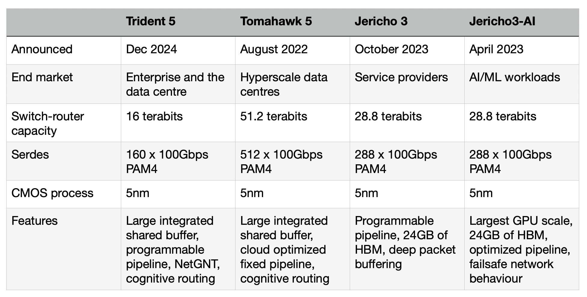
Trident family
Trident is one of Broadcom’s main three lines of networking and switch chips, the Jericho and Tomahawk being the other two.
Service providers favour the Jericho family for high-end IP routing applications. The Ethernet switch router chip’s features include a programmable pipeline and off-chip store for large traffic buffering and look-up tables.
The latest Jericho 3, the 28.8 terabits-per-sec (Tbps) Jericho 3, was announced in September. Broadcom launched the first family device, the Jericho3-AI, earlier this year; a chip tailored for AI networking requirements.
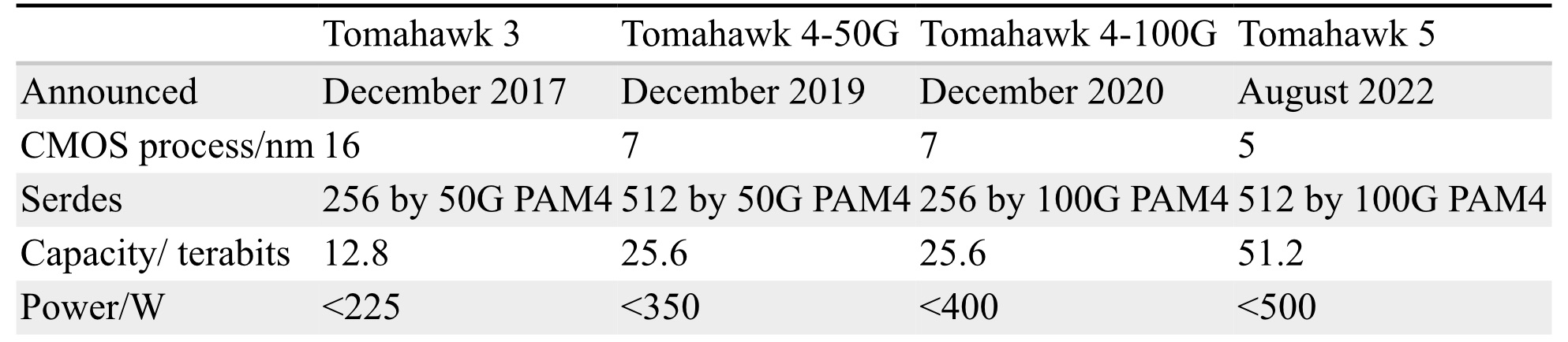
In contrast, Broadcom’s Tomahawk Ethernet network switch family addresses the data centre operators’ needs. The Tomahawk has a relatively simple fixed packet-processing pipeline to deliver the highest switching capacity. The Tomahawk 5 has a capacity of 51.2 terabits and includes 512, 100-gigabit PAM4 serialiser-deserializer (serdes).
“The big hyperscalers want maximum bandwidth and maximum radix [switches],” says Grindley. “The hyperscalers have a pretty simple fabric network and do everything else themselves.”
The third family, the Trident Ethernet switch chips, is popular for enterprise applications. Like the Jericho, the Trident has a programmable pipeline to address enterprise networking tasks such as Virtual Extensible LAN (VXLAN), tunnelling protocols, and segment routing (SRv6).
The speeds and timelines of the various Tomahawk and Trident chips are shown in the chart.

Trident 5-X12
The Trident 5-X12 is implemented using a 5nm CMOS process and has a capacity of 16 terabits. The chip’s input-output includes 160, 100-gigabit PAM4 serdes. These are the serdes that Broadcom introduced with the Tomahawk 5.
The first chip of each new generation of Trident usually has the highest capacity and is followed by lower-capacity devices tailored to particular markets.
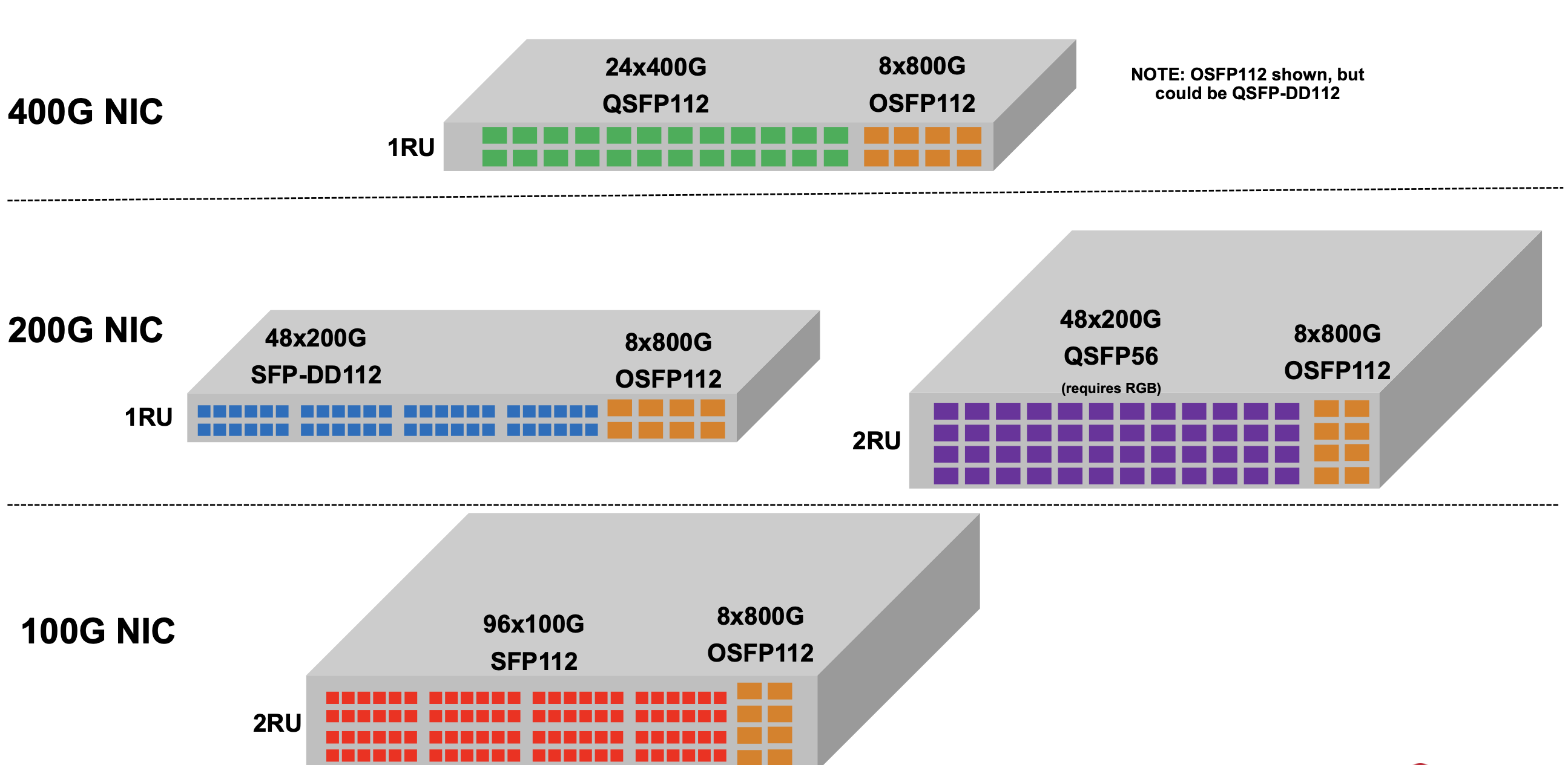
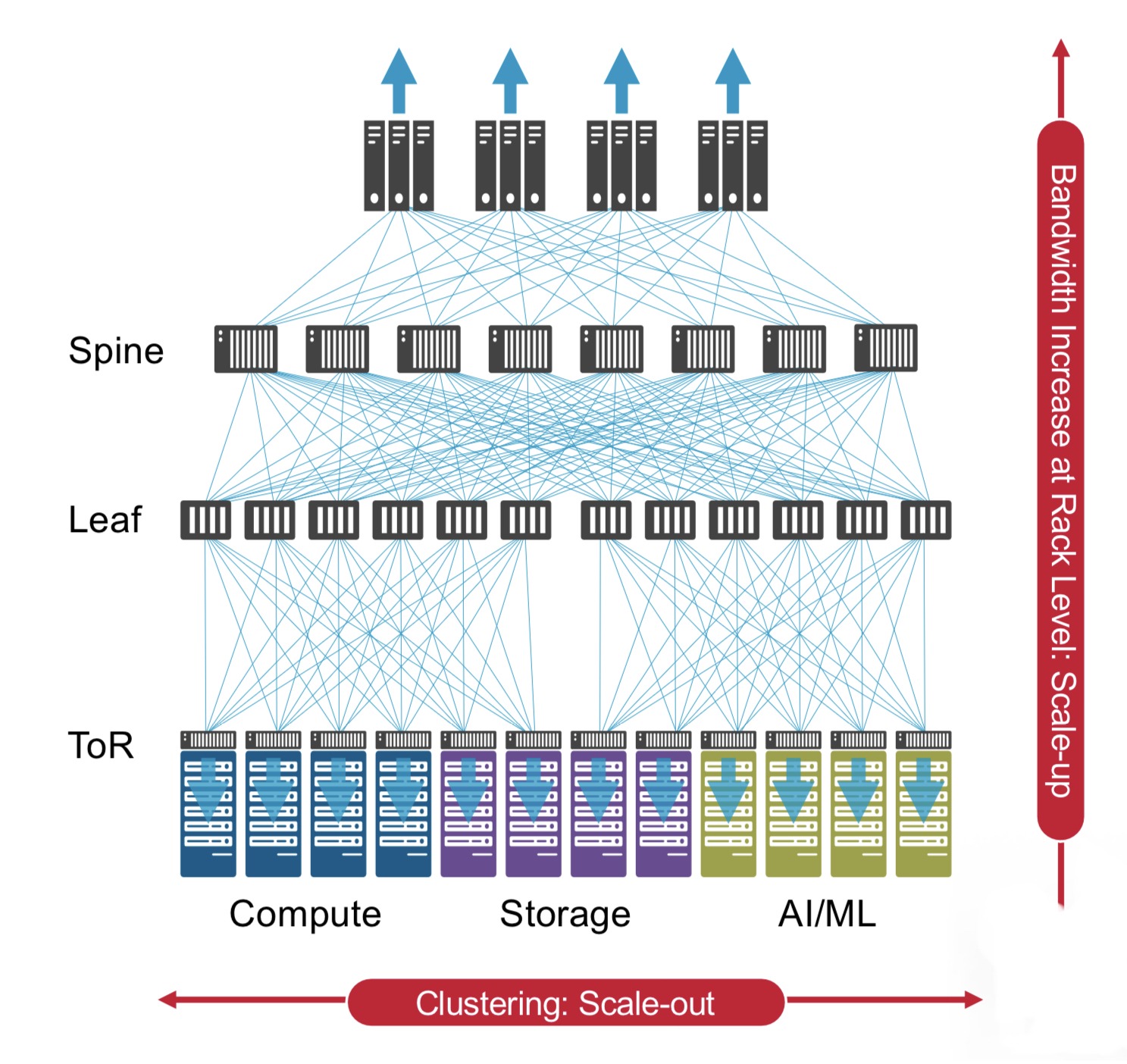
Trident 5 is aimed at top-of-rack switch applications. Typically, 24 or 48 ports of the top-of-rack switch are used for downlinks to connect to servers, while 4 or 8 are used for higher-capacity uplinks (see diagram).
The Trident 5 can support 48 ports of 200 gigabits for the downlinks and eight 800 gigabit for the uplinks. To support 800-gigabit interfaces, the chip uses eight 100-gigabit serdes and an one-chip 800-gigabit media access controller (MAC). Other top-of-rack switch configurations are shown in the diagram.
Currently, 400-gigabit network interface cards are used for demanding applications such as machine learning. Trident5 is also ready to transition to 800-gigabit network interface cards.
Another Tomahawk feature the Trident 5 has adopted is cognitive routing, a collection of congestion management techniques for demanding machine-learning workloads.
One of the techniques is global load balancing. Previous Trident devices supported dynamic load balancing, where the hardware could see the congested port and adapt in real-time. However, such a technique gives no insight into what happens further along the flow path. “If I knew that, downstream, somebody else was congested, then I could make a smarter decision,” says Grindley. Global load balancing does just this. It sends notification to the routing chips upstream that there is congestion so they can all work together.
Another cognitive routing feature is drop congestion notification. Here, packets dropped due to congestion are captured such that what is sent is only their header data and where the packet was dropped. This mechanism improves flow completion times compared to normal packet loss, which is costly for machine-learning workloads.
Trident 5, like its predecessor, Trident 4, has a heterogeneous pipeline of tile types. The tiles contain static random-access memory (SRAM), ternary content-addressable memory (TCAM) or arithmetic logic units. The tiles allow multiple look-ups or actions in parallel at each stage in the pipeline.

Broadcom has a compiler that maps high-level packet-processing functions to its pipeline in the NPL programming language. The latency through the device stays constant, however the packet processing is changed, says Grindley.
Trident 5’s NetGNT inference engine is a new pipeline resource for higher-level traffic patterns. “NexGNT looks at things not at a packet-by-packet level, but across time and the overall packet flow through the network,” says Grindley.
The NetGNT
Until now system architects and network operation centre staff have defined a set of static rules written in software to uncover and treat suspicious packet flows. “A pre-coded set of rules is limited in its ability to catch higher-level traffic patterns,” says Grindley.
When Broadcom started the Trident 5 design, its engineers thought a neural network approach could be used. “We knew it would be useful if you had something that looked at a higher level, and we knew neural networks could do this kind of task,” says Grindley.
The neural network sits alongside the existing traffic analysis logic. Information such as packet headers, or data already monitored and generated by the pipeline, can be fed to the neural network to assess the traffic patterns.
“It sits there and looks for high-level patterns such as the start of a denial of service attack” says Grindley.
Training
The neural network is trained using supervised learning. A human expert must create the required training data and train the model using supervised learning. The result is a set of weights loaded onto the Trident 5’s neural network.

When the neural network is triggered, i.e. when it identifies a pattern of interest, the Trident 5 must decide what it should do. The chip can drop the packets or change the quality of service (QoS). The device can also drop a packet while creating a mirror packet containing headers and metadata. This can then be sent to a central analyser at the network operations centre to perform higher-level management algorithms.
Performance
The Trident 5 chip is now sampling. Broadcom says there is no performance data as end customers are still to train and run live traffic through the Trident 5’s inference engine.
“What it can do for them depends on getting good data and then running the training,” says Grindley. “Nobody has done this yet.”
Will the inference engine be used in other Broadcom networking chips?
“It depends on the market,” says Grindley. “We can replicate it, just like taking IP from the Tomahawk where appropriate.”
Taking a unique angle to platform design

- A novel design based on a vertical line card shortens the trace length between an ASIC and pluggable modules.
- Reducing the trace length improves signal integrity while maintaining the merits of using pluggables.
- Using the vertical line card design will extend for at least two more generations the use of pluggables with Ethernet switches.
The travelling salesperson problem involves working out the shortest route on a round-trip to multiple cities. It’s a well-known complex optimisation problem.
Novel design that shortens the distance between an Ethernet switch chip and the front-panel optics
Systems engineers face their own complex optimisation problem just sending an electrical signal between two points, connecting an Ethernet switch chip to a pluggable optical module, for example.
Sending the high-speed signal over the link with sufficient fidelity for its recovery requires considerable electronic engineering design skills. And with each generation of electrical signalling, link distances are getting shorter.
In a paper presented at the recent ECOC show, held in Basel, consultant Chris Cole, working with Yamaichi Electronics, outlined a novel design that shortens the distance between an Ethernet switch chip and the front-panel optics.
The solution promises headroom for two more generations of high-speed pluggables. “It extends the pluggable paradigm very comfortably through the decade,” says Cole.
Since ECOC, there are plans to standardise the vertical line card technology in one or more multi-source agreements (MSAs), with multiple suppliers participating.
“This will include OSFP pluggable modules as well as QSFP and QSFP-DD modules,” says Cole.
Shortening links
Rather than the platform using stacked horizontal line cards as is common today, Cole and Yamaichi Electronics propose changing the cards’ orientation to the vertical plane.
Vertical line cards also enable the front-panel optical modules to be stacked on top of each other rather than side-by-side. As a result, the pluggables are closer to the switch ASIC; the furthest the high-speed electrical signalling must travel is three inches (7.6cm). The most distant span between the chip and the pluggable with current designs is typically nine inches (22.8cm).
“The reason nine inches is significant is that the loss is high as we reach 200 gigabits-per-second-per-lane and higher,” says Cole.
Current input-output proposals
The industry is pursuing several approaches to tackle such issues as the issues associated with high-speed electrical signalling and also input-output (I/O) bandwidth density.
One is to use twinaxial cabling instead of electrical traces on a printed circuit board (PCB). Such ‘Twinax’ cable has a lower loss, and its use avoids developing costly advanced-material PCBs.
Other approaches involve bringing the optics closer to the Ethernet switch chip, whether near-packaged optics or the optics and chip are co-packaged together. These approaches also promise higher bandwidth densities.
Cole’s talk focussed on a solution that continues using pluggable modules. Pluggable modules are a low-cost, mature technology that is easy to use and change.
However, besides the radio frequency (RF) challenges that arise from long electrical traces, the I/O density of pluggables is limited due to the size of the connector, while placing up to 36 pluggables on the 1 rack unit-high (1RU) front panel obstructs the airflow used for cooling.
Platform design
Ethernet switch chips double their capacity every two years. Their power consumption is also rising; Broadcom’s latest Tomahawk 5 consumes 500W.
The power supply a data centre can feed to each platform has an upper limit. It means fewer cards can be added to a platform if the power consumed per card continues to grow.
The average power dissipation per rack is 16kW, and the limit is around 32kW, says Cole. This refers to when air cooling is used, not liquid cooling.
He cites some examples.
A rack of Broadcom’s 12.8-terabit Tomahawk 3 switch chip – either with 32, 1RU or 16, 2RU cards with two chips per card – and associated pluggable optics consume over 30kW.
A 25.6-terabit Tomahawk 4-based chassis supports 16 line cards and consumes 28kW. However, using the recently announced Tomahawk 5, only eight cards can be supported, consuming 27KW.
“The takeaway is that rack densities are limited by power dissipation rather than the line card’s rack unit [measure],” says Cole.
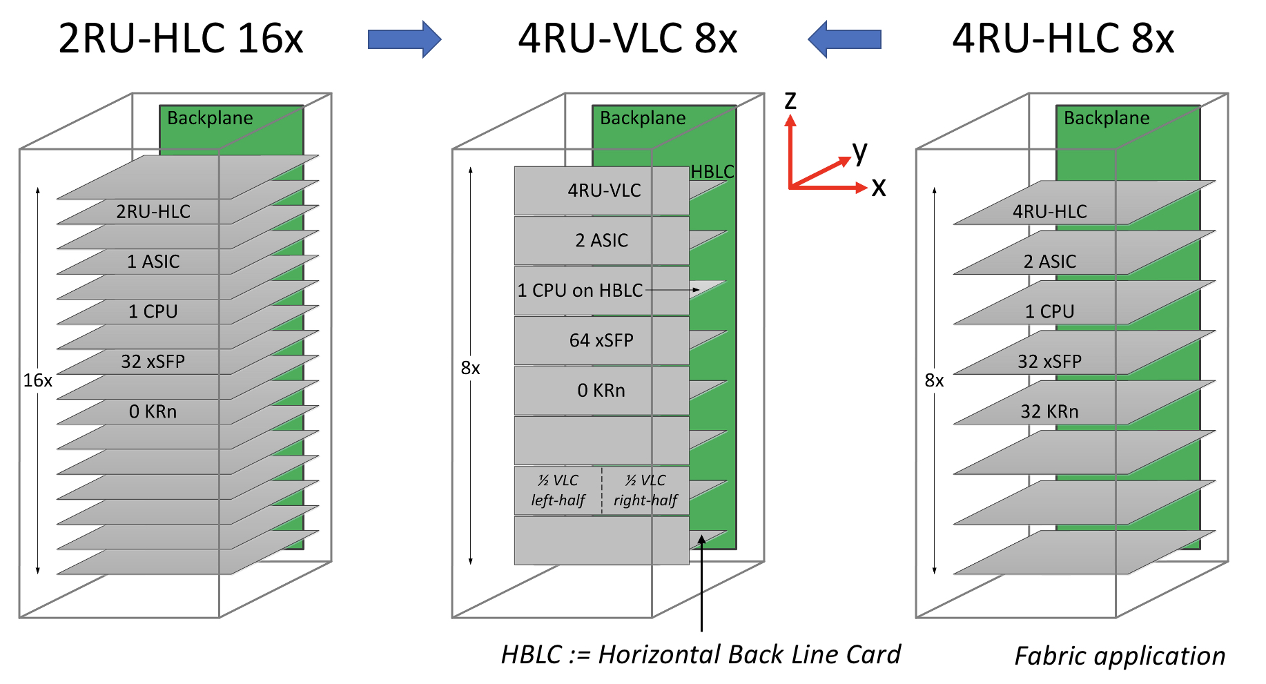
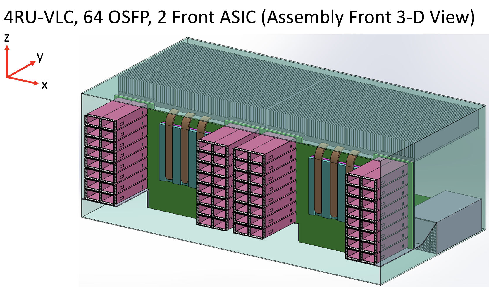
Vertical line card
The vertical line card design is 4RU high. Each card supports two ASICs on one side and 64 cages for the OSFP modules on the other.
A 32RU chassis can thus support eight vertical cards or 16 ASICs, equivalent to the chassis with 16 horizontal 2RU line cards.
The airflow for the ASICs is improved, enabling more moderate air fans to be used compared to 1RU or 2RU horizontal card chassis designs. There is also airflow across the modules.
“The key change in the architecture is the change from a horizontal card to a vertical card while maintaining the pluggable orientation,” says Cole.
As stated, the maximum distance between an ASIC and the pluggables is reduced to three inches, but Cole says the modules can be arranged around the ASIC to minimise the length to 2.5 inches.
Alternatively, if the height of the vertical card is an issue, a 3RU card can be used instead, which results in a maximum trace length of 3.5 inches. “[In this case], we don’t have dedicated air intakes for the CPU,” notes Cole.
Cole also mentioned the option of a 3RU vertical card that houses one ASIC and 64 OSFP modules. This would be suitable for the Tomahawk 5. However, here the maximum trace length is five inches.
Vertical connectors
Yamaichi Electronics has developed the vertical connectors needed to enable the design.
Cole points out that, unlike a horizontal connector, a vertical one uses equal-length contacts. This is not the case for a flat connector, resulting in performance degradation since a set of contacts has to turn and hence has a longer length.
Cole showed the simulated performance of an OSFP vertical connector with an insertion loss of over 70GHz.
“The loss up to 70GHz demonstrates the vertical connector advantage because it is low and flat for all the leads,” says Cole. “So this [design] is 200-gigabit ready.”
He also showed a vertical connector for the OSFP-XD with a similar insertion loss performance.
Also shown was a comparison with results published for Twinax cables. Cole says this indicates that the loss of a three-inch PCB trace is less than the loss of the cable.
“We’ve dramatically reduced the RF maximum length, so we had solved the RF roadblock problem, and we maintain the cost-benefit of horizontal line cards,” says Cole.
The I/O densities may be unchanged, but it preserves the mature technology’s benefits. “And then we get a dramatic improvement in cooling because there are no obstructions to airflow,” says Cole.
Vladimir Kozlov, CEO of the market research firm, LightCounting, wondered in a research note whether the vertical design is a distraction for the industry gearing up for co-packaged optics.
“Possibly, but all approaches for reducing power consumption on next-generation switches deserve to be tested now,” said Kozlov, adding that adopting co-packaged optics for Ethernet switches will take the rest of the decade.
“There is still time to look at the problem from all angles, literally,” said Kozlov

Tencent makes its co-packaged optics move

- Tencent is the first hyperscaler to announce it is deploying a co-packaged optics switch chip
- Tencent will use Broadcom’s Humboldt that combines its 25.6-terabit Tomahawk 4 switch chip with four optical engines, each 3.2 terabit-per-second (Tbps)
Part 2: Broadcom’s co-packaged optics
Tencent will use Broadcom’s Tomahawk 4 switch chip co-packaged with optics for its data centres.
“We are now partnered with the hyperscaler to deploy this in a network,” says Manish Mehta, vice president of marketing and operations optical systems division, Broadcom. “This is a huge step for co-packaged optics overall.”
Broadcom demonstrated a working version of a Humboldt switch at OFC earlier this year.
The Chinese hyperscaler will use Broadcom’s 25.6Tbps Tomahawk 4 Humboldt, a hybrid design where half of the chip’s input-output (I/O) is optical and half is the chip’s serialisers-deserialisers (serdes) that connect to pluggable modules on the switch’s front panel.
Four Broadcom 3.2-terabit silicon photonics-based optical engines are co-packaged alongside the Tomahawk 4 chip to implement 12.8Tbps of optical I/O.
Broadcom demonstrated a working version of a Humboldt switch at OFC earlier this year.
Co-packaged optics
Broadcom started its co-packaged optics development work in 2019.
“One of the reasons for our investment in co-packaged optics was that we did see firsthand the ongoing limits of copper interconnect being approached,” says Mehta.
The transmission reach of copper links continues to shrink as the signalling speed has increased from 25 gigabits-per-second (Gbps) non-return to zero (NRZ) to PAM-4 (4-level pulse amplitude modulation) based signalling at 56Gbps, 112Gbps and, in the coming years, 224Gbps. Power consumption is also rising with each speed hike.
Broadcom says data centres now use 1 million optical interconnects, but that much of the connectivity is still copper-based, linking adjacent racks and equipment within the rack.
“Hyperscalers spend ten times more on interconnects than switching silicon,” says Mehta. Given these trends, there needs to be a continual improvement in the power profile, cost and scaled manufacturing of optical interconnect, he says.
In the short term, what is driving interest in co-packaged optics is overcoming the limitations of copper, says Broadcom.
In early 2021, Broadcom detailed at a JP Morgan event its co-packaged optics roadmap. Outlined was the 25.6-terabit Humboldt to be followed by Bailly, a 51.2-terabit all co-packaged optics design using Broadcom’s Tomahawk 5 switch chip which is now sampling.
Humboldt uses DR4 (4×100-gigabit using 4 fibres) whereas the 51.2-terabit Bailly will add multiplexing-demultiplexing and use the FR4 specification (4×100-gigabit wavelengths per fibre).
Technology and partners
Broadcom’s in-house technology includes lasers (VCSELs and EMLs), mixed-signal expertise (trans-impedance amplifiers and drivers), and silicon photonics, as well as its switch chips.
Broadcom uses a remote laser source for its co-packaged optics design. Placing the laser away from the package (the switch chip and optics) means no cooling is needed.
Broadcom is working with 15 partners to enable its co-packaged optics, highlighting the breadth of expertise required and the design complexity.
There are two prominent use cases for the hybrid I/O Humboldt.
One is for top-of-rack switches, where the electrical interfaces support short-reach copper links connecting the servers in a rack, while the optical links connect the top-of-rack box to the next layer of aggregation switching.
The second use is at the aggregation layer, where the electrical I/O connects other switches in the rack while the optical links connect to switch layers above or below the aggregation layer.
“There is a use case for having pluggable ports where you can deploy low-cost direct-attached copper,” says Mehta.
Broadcom says each data centre operator will have their own experience with their manufacturing partners as they deploy co-packaged optics. Tencent has decided to enter the fray with 25.6-terabit switches.
“It is not just Broadcom developing the optical solution; it is also ensuring that our manufacturing partner is ready to scale,” says Mehta.
Ruijie Networks is making the two-rack-unit (2RU) switch platform for Tencent based on Broadcom’s co-packaged optics solution. The co-packaged optics interfaces are routed to 16 MPO connectors while the switch supports 32, 400-gigabit QSFP112 modules.
“It’s always important to have your lead partner [Tencent] for any deployment like this, someone you’re working closely with to get it to market,” says Mehta. “But there is interest from other customers as well.”
Cost and power benefits
Broadcom says co-packaged optics will lower the optical cost-per-bit by 40 per cent while the system (switch platform) power savings will be 30 per cent.
Humboldt more than halves the power compared to using pluggables. Broadcom’s co-packaged optics consumes 7W for each 800-gigabits of bandwidth, whereas an equivalent 800-gigabit optical module consumes 16-18W.
Its second-generation design will embrace 5nm CMOS rather than 7nm and still more than halve the power: an 800-gigabit pluggable will consume 14-15W, whereas it will be 5.5W for the same co-packaged optics bandwidth.
Broadcom will move to CMOS for its second-generation electrical IC; it uses silicon germanium at present.
Power and operational cost savings are a longer-term benefit for data centre operators, says Broadcom. A more immediate concern is the growing challenge of managing the thermal profile when designing switching systems. “The amount of localised heat generation of these components is making systems quite challenging,” says Mehta.
A co-packaged design eliminates pluggables, making system design easier by improving airflow via the front panel and reducing the power required for optical interconnect.
“They’ve been telling us this directly,” says Mehta. “It’s been a pretty good testimonial to the benefits they can see for system design and co-packaged optics.”
Roadmap
At OFC 2022, Broadcom also showed a mock-up of Bailly, a 51.2 terabit switch chip co-packaged with eight 6.4Tbps optical engines.
Broadcom will offer customers a fully co-packaged optics Tomahawk 5 design but has not given a date.
Since Broadcom has consistently delivered a doubling of switch silicon capacity every 24 months, a 102.4-terabit Tomahawk 6 is scheduled to sample in the second half of 2024.
That timescale suggests it will be too early to use 224Gbps serdes being specified by the OIF. Indeed, Mehta believes 112Gbps serdes will have “a very long life”.
That would require the next-generation 102.2Tbps to integrate 1024, 100Gbps serdes on a die. Or, if that proves too technically challenging, then, for the first time, Broadcom’s switching ASIC may no longer be a monolithic die.
Broadcom’s networking group is focused on high-speed serial electrical interfaces. But the company is encouraged by developments such as the open standard UCIe for package interconnect, which looks at slower, wider parallel electrical interfaces to support chiplets. UCIe promises to benefit co-packaged optics.
Broadcom’s view is that it is still early with many of these design challenges.
“Our goal is to understand when we need to be ready and when we need to be launching our silicon on the optical side,” says Mehta. “That’s something we are working towards; it’s still not clear yet.”

Broadcom samples the first 51.2-terabit switch chip

- Broadcom’s Tomahawk 5 marks the era of the 51.2-terabit switch chip
- The 5nm CMOS device consumes less than 500W
- The Tomahawk 5 uses 512, 100-gigabit PAM-4 (4-level pulse amplitude modulation) serdes (serialisers-deserialisers)
- Broadcom will offer a co-packaged version combining the chip with eight 6.4 terabit-per-second (Tbps) optical engines
Part 1: Broadcom’s Tomahawk 5
Broadcom is sampling the world’s first 51.2-terabit switch chip.
With the Tomahawk 5, Broadcom continues to double switch silicon capacity every 24 months; Broadcom launched the first 3.2-terabit Tomahawk was launched in September 2014.
“Broadcom is once again first to market at 51.2Tbps,” says Bob Wheeler, principal analyst at Wheeler’s Network. “It continues to execute, while competitors have struggled to deliver multiple generations in a timely manner.”
Tomahawk family
Hyperscalers use the Tomahawk switch chip family in their data centres.
Broadcom launched the 25.6-terabit Tomahawk 4 in December 2019. The chip uses 512 serdes, but these are 50-gigabit PAM-4. At the time, 50-gigabit PAM-4 matched the optical modules’ 8-channel input-output (I/O).
Certain hyperscalers wanted to wait for 400-gigabit optical modules using four 100-gigabit PAM-4 electrical channels, so, in late 2020, Broadcom launched the Tomahawk4-100G switch chip, which employs 256, 100-gigabit PAM-4 serdes.
Tomahawk 5 doubles the 100-gigabit PAM-4 serdes to 512. However, given that 200-gigabit electrical interfaces are several years off, Broadcom is unlikely to launch a second-generation Tomahawk 5 with 256, 200-gigabit PAM-4 serdes.
Switch ICs
Broadcom has three switch chip families: Trident, Jericho and the Tomahawk.
The three switch chip families are needed since no one switch chip architecture can meet all the markets’ requirements.
With its programable pipeline, Trident targets enterprises, while Jericho targets service providers.
According to Peter Del Vecchio, Broadcom’s product manager for the Tomahawk and Trident lines, there is some crossover. For example, certain hyperscalers favour the Trident’s programmable pipeline for their top-of-rack switches, which interface to the higher-capacity Tomahawk switches chips at the aggregation layer.
Monolithic design
The Tomahawk 5 continues Broadcom’s approach of using a monolithic die design.
“It [the Tomahawk5] is not reticule-limited, and going to [the smaller] 5nm [CMOS process] helps,” says Del Vecchio.
The alternative approach – a die and chiplets – adds overall latency and consumes more power, given the die and chiplets must be interfaced. Power consumption and signal delay also rise whether a high-speed serial or a slower, wider parallel bus is used to interface the two.
Equally, such a disaggregated design requires an interposer on which the two die types sit, adding cost.
Chip features
Broadcom says the capacity of its switch chips has increased 80x in the last 12 years; in 2010, Broadcom launched the 640-gigabit Trident.
Broadcom has also improved energy efficiency by 20x during the same period.
“Delivering less than 1W per 100Gbps is pretty astounding given the diminishing benefits of moving from a 7nm to a 5nm process technology,” says Wheeler.
“In general, we have achieved a 30 per cent plus power savings between Tomahawk generations in terms of Watts-per-gigabit,” says Del Vecchio.

These power savings are not just from advances in CMOS process technology but also architectural improvements, custom physical IP designed for switch silicon and physical design expertise.
“We create six to eight switch chips every year, so we’ve gotten very good at optimising for power,” says Del Vecchio
The latest switch IC also adds features to support artificial intelligence (AI)/ machine learning, an increasingly important hyperscaler workload.
AI/ machine learning traffic flows have a small number of massive ‘elephant’ flows alongside ‘mice’ flows. The switch chip adds elephant flow load balancing to tackle congestion that can arise when the two flow classes mix.
“The problem with AI workloads is that the flows are relatively static so that traditional hash-based load balancing will send them over the same links,” says Wheeler. “Broadcom has added dynamic balancing that accounts for link utilisation to distribute better these elephant flows.”
The Tomahawk 5 also provides more telemetry information so data centre operators can better see and tackle overall traffic congestion.
The chip has added virtualisation support, including improved security of workloads in a massively shared infrastructure.
Del Vecchio says that with emerging 800-gigabit optical modules and 1.6 terabit ones on the horizon, the Tomahawk 5 is designed to handle multiples of 400 Gigabit Ethernet (GbE) and will support 800-gigabit optical modules.
The chip’s 100-gigabit physical layer interfaces are combined to form 800 gigabit (8 by 100 gigabit), which is fed to the MAC, packet processing pipeline and the Memory Management Unit to create a logical 800-gigabit port. “After the MAC, it’s one flow, not at 400 gigabits but now at 800 gigabits,” says Del Vecchio.
Market research firm, Dell’Oro, says that 400GbE accounts for 15 per cent of port revenues and that by 2026 it will rise to 57 per cent.
Broadcom also cites independent lab test data showing that its support for RDMA over Converged Ethernet (RoCE) matches the performance of Infiniband.
“We’re attempting to correct the misconception promoted by competition that Infiniband is needed to provide good performance for AI/ machine learning workloads,” says Del Vecchio. The tests used previous generation silicon, not the Tomahawk 5.
“We’re saying this now since machine learning workloads are becoming increasingly common in hyperscale data centres,” says Del Vecchio.
As for the chip’s serdes, they can drive 4m of direct attached copper cabling, with sufficient reach to connect equipment within a rack or between two adjacent racks.
Software support
Broadcom offers a software development kit (SDK) to create applications. The same SDK is common to all three of its switch chip families.
Broadcom also supports the Switch Abstraction Interface (SAI). This standards-based programming interface sits on top of the SDK, allowing the programming of switches independent of the silicon provider.
Broadcom says some customers prefer to use its custom SDK. It can take time for changes to filter up, and a customer may want something undertaken that Broadcom can develop quickly using its SDK.
System benefits
Doubling the switch chip’s capacity every 24 months delivers system benefits.That is because implementing a 51.2-terabit switch using the current generation Tomahawk 4 requires six such devices.

Now a single 2-rack-unit (2RU) Tomahawk 5 switch chip can support 64 by 800-gigabit, 128 by 400-gigabit and 256 by 200-gigabit modules.
These switch boxes are air-cooled, says Broadcom.
Co-packaged optics
In early 2021 at a J.P Morgan analyst event, Broadcom revealed its co-packaged optics roadmap that highlighted Humboldt, a 25.6-terabit switch chip co-packaged with optics, and Bailly, a 51.2-terabit fully co-packaged optics design.
At OFC 2022, Broadcom demonstrated a 25.6Tbps switch that sent half of the traffic using optical engines.
Also shown was a mock-up of Bailly, a 51.2 terabit switch chip co-packaged with eight optical engines, each at 6.4Tbps.
Broadcom will offer customers a fully co-packaged optics Tomahawk 5 design but has not yet given a date.
Broadcom can also support a customer if they want tailored connectivity with, say, 3/4 of the Tomahawk 5 interfaces using optical engines and the remainder using electrical interfaces to front panel optics.