
Imec eyes silicon photonics to solve chip I/O bottleneck
In the second and final article, the issue of adding optical input-output (I/O) to ICs is discussed with a focus on the work of the Imec nanoelectronics R&D centre that is using silicon photonics for optical I/O.
Part 2: Optical I/O
Imec has demonstrated a compact low-power silicon-photonics transceiver operating at 40 gigabits per second (Gbps). The silicon photonics transceiver design also uses 14nm FinFET CMOS technology to implement the accompanying driver and receiver electronics.
 Joris Van Campenhout“We wanted to develop an optical I/O technology that can interface to advanced CMOS technology,” says Joris Van Campenhout, director of the optical I/O R&D programme at Imec. “We want to directly stick our photonics device to that mainstream CMOS technology being used for advanced computing applications.”
Traditionally, the Belgium nanoelectronics R&D centre has focussed on scaling logic and memory but in 2010 it started an optical I/O research programme. “It was driven by the fact that we saw that electrical I/O doesn’t scale that well,” says Van Campenhout. Electrical interfaces have power, space and reach issues that get worse with each hike in transmission speed.
Imec is working with partner companies to research optical I/O. The players are not named but include semiconductor foundries, tool vendors, fabless chip companies and electronic design automation tools firms. The aim is to increase link capacity, bandwidth density - a measure of the link capacity that can be crammed in a given space - and reach using optical I/O. The research’s target is to achieve between a 10x to 100x in scaling.
The number of silicon photonics optical I/O circuits manufactured each year remains small, says Imec, several thousand to ten thousand semiconductor wafers at most. But Imec expects volumes to grow dramatically over the next five years as optical interconnects are used for ever shorter reaches, a few meters and eventually below one meter.
“That is why we are participating in this research, to put together building blocks to help in the technology pathfinding,” says Van Campenhout.
We wanted to develop an optical I/O technology that can interface to advanced CMOS technology
Silicon photonics transceiver
Imec has demonstrated a 1330nm optical transceiver operating at 40Gbps using non-return-to-zero signalling. The design uses hybrid integration to combine silicon photonics with 14nm FinFET CMOS electronics. The resulting transceiver occupies 0.025 mm2, the area across the combined silicon photonics and CMOS stack for a single transceiver channel. This equates to a bandwidth density of 1.6 terabit-per-second/mm2.
The silicon photonics and FinFET test chips each contain circuitry for eight transmit and eight receive channels. Combined, the transmitter path comprises a silicon photonics ring modulator and a FinFET differential driver while the receiver uses a germanium-based photo-detector and a first-stage FinFET trans-impedance amplifier (TIA).
The transceiver has an on-chip power consumption of 230 femtojoules-per-bit, although Van Campenhout stresses that this is a subset of the functionality needed for the complete link. “This number doesn’t include the off-chip laser power,” he says. “We still need to couple 13dBm - 20mW - of optical power in the silicon photonics chip to close the link budget.” Given the laser has an efficiency of 10 to 20 percent, that means another 100mW to 200mW of power.
That said, an equivalent speed electrical interface has an on-chip power consumption of some 2 picojoules-per-bit so the optical interface still has some margin to better the power efficiency of the equivalent electrical I/O. In turn, the optical I/O’s reach using single-mode fibre is several hundred meters, far greater than any electrical interface.
Imec is confident it can increase the optical interface’s speed to 56Gbps. The layout of the CMOS circuits can be improved to reduce internal parasitic capacitances while Imec has already improved the ring modulator design compared to the one used for the demonstrator.
“We believe that with a few design tweaks we can get to 56Gbps comfortably,” says Van Campenhout. “After that, to go faster will require new technology like PAM-4 rather than non-return-to-zero signalling.”
Imec has also tested four transmit channels using cascaded ring modulators on a common waveguide as part of work to add a wavelength-division multiplexing capability.
Transceiver packaging
The two devices - the silicon photonics die and the associated electronics - are combined using chip-stacking technology.
Both devices use micro-bumps with a 50-micron pitch with the FinFET die flip-chipped onto the silicon photonics die. The combined CMOS and silicon photonics assembly is glued on a test board and wire-bonded, while the v-groove fibre arrays are attached using active alignment. The fibre-to-chip coupling loss, at 4.5dB in the demonstration, remains high but the researchers say this can be reduced, having achieved 2dB coupling losses in separate test chips.
 Source: Imec.
Imec is also investigating using through-silicon vias (TSV) technology and a silicon photonics interposer in order to replace the wire-bonding. TSVs deliver better power and ground signals to the two dies and enable high-speed electrical I/O between the transceiver and the ASIC such as a switch chip. The optics and ASIC could be co-packaged or the transceiver used in an on-board optics design next to the chip.
“We have already shown the co-integration of TSVs with our own silicon photonics platform but we are not yet showing the integration with the CMOS die,” says Van Campenhout. “Something we are working on.”
Co-packaging the optics with silicon will come at a premium cost
Applications
The first ICs to adopt optical I/O will be used in the data centre and for high-performance computing. The latest data centre switch ICs, with a capacity of 12.8 terabits, are implemented using 16nm CMOS. Moving to a 7nm CMOS process node will enable capacities of 51.2 terabits. “These are the systems where the bandwidth density challenge is the largest,” says Van Campenhout.
But significant challenges must be overcome before this happens, he says: “I think we all agree that bringing optics deeply integrated into such a product is not a trivial thing.”
Co-packaging the optics with silicon will come at a premium cost. There are also reliability issues to be resolved and greater standardisation across the industry will be needed as to how the packaging should be done.
Van Campenhout expects this will only happen in the next four to five years, once the traffic-handling capacity of switch chips doubles and doubles again.
Imec has seen growing industry interest in optical I/O in the last two years. “We have a lot of active interactions so interest is accelerating now,” says Van Campenhout.
Ciena goes stackable with 8180 'white box' and 6500 RLS
Ciena has unveiled two products - the 8180 coherent networking platform and the 6500 reconfigurable line system - that target cable and cellular operators that are deploying fibre deep in their networks, closer to subscribers.
The 6500 line system is also aimed at the data centre interconnect market given how the webscale players are experiencing a near-doubling of traffic each year.
 Source: Ciena
The cable industry is moving to a distributed access architecture (DAA) that brings fibre closer to the network’s edge and splits part of the functionality of the cable modem termination system (CMTS) - the remote PHY - closer to end users. The cable operators are deploying fibre to boost the data rates they can offer homes and businesses.
Both Ciena’s 8180 modular switch and the 6500 reconfigurable line system are suited to the cable network. The 8180 is used to link the master headend with primary and secondary hub sites where aggregated traffic is collected from the digital nodes (see network diagram). The 8180 platforms will use the modular 6500 line system to carry the dense wavelength-division multiplexed (DWDM) traffic.
 “The [cable] folks that are modernising the access network are not used to managing optical networking,” says Helen Xenos, senior director, portfolio marketing at Ciena (pictured). “They are looking for simple platforms, aggregating all the connections that are coming in from the access.”
The 8180 can play a similar role for wireless operators, using DWDM to carry aggregated traffic for 4G and 5G networks.
Ciena says the 6500 optical line system will also serve the data centre interconnect market, complementing the WaveServer Ai, Ciena’s second-generation 1RU modular platform that has 2.4 terabits of client-side interfaces and 2.4 terabits of coherent capacity.
With the 8180, you are only using the capacity on the fibre that you have traffic for
“They [the webscale players] are looking for as many efficiencies as they can get from the platforms they deploy,” says Xenos. “The 6500 reconfigurable line system gives them the flexibility they need - a colourless, directionless, contentionless [reconfigurable optical add-drop multiplexer] and a flexible grid that extends to the L-band.”
A research note from analyst house, Jefferies, published after the recent OFC show where Ciena announced the platforms, noted that in many cable networks, 6-strand fibre is used: two fibre pairs allocated for business services and one for residential. Adding the L-band to the existing C-band effectively doubles the capacity of each fibre pair, it noted.
The 8180
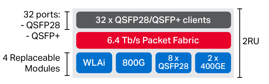
Ciena’s 8180 is a modular packet switch that includes coherent optics. The 8180 is similar in concept to the Voyager and Cassini white boxes developed by the Telecom Infra Project. However, the 8180 is a two-rack-unit (2RU) 6.4-terabit switch compared to the 1RU, 2-terabit Voyager and the 1.5RU 3.2-terabit Cassini. The 8180 also uses Ciena’s own 400-gigabit coherent DSP, the WaveLogic Ai, rather than merchant coherent DSP chips.
The platform comprises 32 QSFP+/ QSFP28 client-side ports, a 6.4-terabit switch chip and four replaceable modules or ‘sleds’, each capable of accommodating 800 gigabits of capacity. The options include an initial 400-gigabit line-side coherent interface (a sled with two coherent WaveLogic Ai DSPs will follow), an 8x100-gigabit QSFP28 sled, a 2x400-gigabit sled and also the option for an 800-gigabit module once they become available.
 Source: Ciena
Using all four sleds as client-side options, the 8180 becomes a 6.4-terabit Ethernet switch. Using only coherent sleds instead, the packet-optical platform has a 1.6-terabit line-side capacity. And because there is a powerful switch chip integrated, the input ports can be over-subscribed.“With the 8180, you are only using the capacity on the fibre that you have traffic for,” says Xenos.
6500 line system
The 6500 reconfigurable line system is also a modular design. Aimed at the cable, wireless, and data centre interconnect markets, only a subset of Ciena’s existing optical line systems features is used.
“The 6500 software has a lot of capabilities that the content providers are not using,” says Xenos. “They just want to use it as a photonic layer.”
There are three 6500 reconfigurable line system platform sizes: 1RU, 2RU and 4RU. The chassis can be stacked and managed as one unit. Card options that fit within the chassis include amplifiers and reconfigurable optical add-drop multiplexers (ROADMs).
The amplifier options area dual-line Erbium-doped fibre amplifiercard that includes an integrated bi-directional optical time-domain reflectometer (OTDR) used to characterise the fibre. There is also a half-line-width RAMAN amplifier card. The line system will support the C and L bands, as mentioned.
The reconfigurable line system also has ROADM cards: a 1x12 wavelength-selective switch (WSS) with integrated amplifier, a colourless 16-channel add-drop that support channels of any size (flexible grid), and a full-width card 1x32 WSS. “The 1x32 would be used for colourless, directionless and directionless [ROADM] configurations,” says Xenos.
The 6500 reconfigurable line system also supports open application porgramming interfaces (APIs) for telemetry, with a user able to program the platform to define the data streamed.“The platform can also be provisioned via REST APIs; something a content provider will do,” she says.
Ciena is a member of the OpenROADM multi-source agreement and was involved in last year’s AT&T OpenROADM trial with its 6500 Converged Packet Optical Transport (POTS) platform.
Will the 6500 reconfigurable line system be OpenROADM-compliant?
“This card [and chassis form factor] could be used for OpenROADM if AT&T preferred this platform to the other [6500 Converged POTS] one,” says Xenos. “You also have to design the hardware to meet the specifications for OpenROADM.”
Ciena expects both platforms to be available by year-end. The 6500 reconfigurable line system will be in customer trials at the end of this quarter while the 8180 will be trialed by the end of the third quarter.