Teramount brings pluggability to co-packaged optics
Hesham Taha, the CEO and co-founder of Teramount, describes the last two years for his company as eventful.
“Many things have happened on many fronts,” he says.
Teramount has developed a fibre assembly technology for designs integrating photonics and chips.
The start-up has raised $20 million in funding and has 30 staff. In addition, the company is recruiting staff experienced in manufacturing processes.
“The funding helps to support what we are working on today, which is manufacturing readiness,” says Taha.
Taha also notes marketplace changes as when the rising interest in co-packaged caused some companies that had stepped out of silicon photonics to return.
The marketplace moves reflect silicon photonics’ changing role. The technology is central for integrated designs such as co-packaged optics, whereas before, it had a more peripheral role when used for pluggable optics.
“This is a big change that requires optical integration with electronics, a change in packaging, and how you assemble fibres,” says Taha.
Plugs and bumps
Teramount’s technology coupling fibre to silicon photonics chips has two elements: a photonic bump and a photonic plug. The two combined avoid having to bond the fibre to the chip directly.
This is important for two reasons.
First, fibre bonding is an extra manufacturing step that impacts adversely the yield of an expensive chip.
Second, the plug, which is on a separate plane from the chip, working together with the photonic bump, enables the fibres to be detached and serviced, much like pluggable optics.
The photonic plug holds the fibres using a V-groove mechanism and couples them to the silicon photonics chip via the photonic bump, a component manufactured as part of the silicon photonics design.
It is the plug and bump combined that deliver large assembly tolerances. “The large tolerances is what enables the detachability,” says Taha.
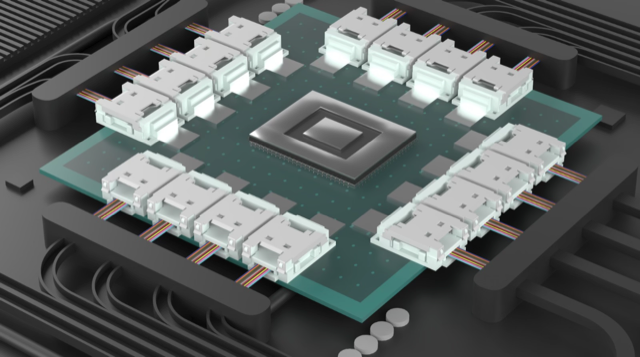
It means a semiconductor company can avoid dealing with fibres and focus on what it does best: designing chips. Foundries and outsourced semiconductor assembly and test (OSAT) companies can handle the wafer-level plug and connect the fibres.
“If the right foundations are set on the silicon photonics wafer, then silicon photonics packaging can become very easy with detachable optics,” says Taha.
Surface coupling and edge coupling
Silicon photonics uses two approaches to couple the optical signal from the fibre to a photonics chip.
One, known as surface coupling, uses a grating coupler, while the second uses side coupling.
Grating couplers are wavelength dependent and send the light beam out at a specific angle. Therefore, changing the wavelength affects the angle, complicating the interfacing.

As part of the silicon photonics chip design, the photonic bump – effectively a lens – is positioned accurately next to the grating coupler.
In contrast, side coupling collects the beam for the silicon photonic chip’s waveguide from the edge of the die. Here, there is no spectral dependency. “You can inject in and out multiple wavelengths,” says Taha.
Teramount says side coupling is not viable for the volume manufacturing of silicon photonic designs.
“You cannot connect a fibre from the edge of the die; you have to prepare for a photonic bump before wafer dicing for side coupling,” says Taha.
Teramount’s design enables light to go to the side of the die, but instead of collecting it from the edge, the photonic bump deflects the beam vertically.
“The photonic bump shifts side coupling into the wideband surface coupling,” says Taha.
The photonic bump has two components in the wideband surface coupling case: a wideband deflector and a lens mirror for beam expansion.
The photonic bump and plug combined forms what Teramount calls self-aligning optics. “You have added more complexity in wafer-level manufacturing, but you have relaxed the tolerances in the assembly domain,” he says.
The resulting design has assembly tolerances of +/- 30 microns. “Altogether, over 60 microns, you lose only half a dB in misalignment tolerances,” he says.
Teramount supports both solutions: surface coupling for a single wavelength and wideband surface coupling for multiple wavelengths. Most customers are working with the wideband solution, says Taha.
The assembly tolerances, wideband surface coupling, and planar separation of the fibres from the die, are what enable fibre detachability, says Taha.
“A technician can manually assemble hundreds of fibres on a co-packaged optics stack,” he says.
The fibre assembly process is compatible with semiconductor packaging techniques. No fibre reflow soldering is needed, improving co-packaged optics’ yield while enabling the servicing of the fibre assembly for co-packaged optics.
Status
Teramount announced in 2022 a collaboration with EV Group, an equipment and process solutions supplier, to tackle wafer-level optics.
Taha says Teramount is working with foundries, OSATs and wafer-level optics manufacturers, such as EV group, to create an ecosystem for its photonic bump and photonic plug technology.
“We want the customer to have the ability to use a foundry to include in their wafer a photonic bump,” says Taha. “Once there, a customer can enjoy the photonic plug connector, its relaxed assembly tolerances, and detachable fibre connectivity.”
Teramount is also working with vendors in networking and computing, developers of co-packaged optics and optical input-output for processor clusters used for machine learning, respectively.
“We’ve already sent samples to customers that we are working with, which includes 32 fibres,” says Taha.
Teramount intends to announce more collaborations with vendors and wafer-manufacturing suppliers.
OFC 2023 show preview
- Sunday, March 5 marks the start of the Optical Fiber Communication (OFC) conference in San Diego, California
- The three General Chairs – Ramon Casellas, Chris Cole, and Ming-Jun Li – discuss the upcoming conference
OFC 2023 will be a show of multiple themes. That, at least, is the view of the team overseeing and coordinating this year’s conference and exhibition.
General Chair Ming-Jun Li of Corning who is also the recipient of the 2023 John Tyndall Award (see profiles, bottom), begins by highlighting the 1,000 paper submissions, suggesting that OFC has returned to pre-pandemic levels.
Ramon Casellas, another General Chair, highlights this year’s emphasis on the social aspects of technology. “We are trying not to forget what we are doing and why we are doing it,” he says.
Casellas highlights the OFC’s Plenary Session speakers (see section, below), an invited talk by Professor Dimitra Simeonidou of the University of Bristol, entitled: Human-Centric Networking and the Road to 6G, and a special event on sustainability.
This year’s OFC has received more submissions on quantum communications totaling 66 papers.
In the past, papers on quantum communications were submitted across OFC’s tracks addressing networking, subsystems and systems, and devices. However, evaluating them was challenging given that only some reviewers are quantum experts, says Chris Cole, the third General Chair. Now, OFC has a subcommittee dedicated to quantum.
Another first is OFCnet, a production network that will run during the show.
Themes and topics
Machine learning is one notable topic this year. The subject is familiar at OFC, says Casellas, but people are discussing it more.
Casellas highlights one session at OFC 2021 that addressed machine learning for optics and optics for machine learning. “It showed the duality of how you can use photonic components to do machine learning and apply machine learning to optimise networking,” says Casellas.
This year there will be additional aspects of machine learning for networks, transmission, and operations, says Casellas.
Other General Chair highlighted subjects include point-to-multipoint coherent transmission, non-terrestrial and satellite networks, and optical switching and how its benefits networking in the data centre.
Google, for example, is presenting a paper detailing its use of optical switching in its data centres, something the hyperscaler disclosed at the ACM Sigcomm conference in August 2022.
There is also more interest in fibre sensors used in communications networks.
“We see an increasing trend because now if you want smart networks, you need sensors everywhere,” says Li.
“That is another theme that goes across all the tracks, which is a non-traditional optical fibre communication area that we’ve been embracing,” adds Cole.
As examples, Cole cites lidar, radio over fibre, free-space communications, microwave fibre sensing, and optical processing.
OFC has had contributions in these areas, he says, but now these topics have dedicated subcommittee titles.
Plenary session
This year’s three Plenary Session speakers are:
- Patricia Obo-Nai, CEO of Vodafone Ghana, who will discuss Harnessing Digitalization for Effective Social Change,
- Jayshree V. Ullal, president and CEO of Arista Networks, addressing The Road to Petascale Cloud Networking,
- and Wendell P. Weeks, chairman and CEO of Corning, whose talk is entitled Capacity to Transform.
“We thought that having someone who could explain how technology improves society would be very positive,” says Casellas. “I’m proud to have someone who can talk on the benefits of digitisation from the point of view of society, in addition to more technical topics.”
Li highlights how OFC celebrated the 50th anniversary of low-loss fibre two years ago and that last year, OFC celebrated the year of glass, displaying information on panels.
Corning has played an important role in both technologies. “Having a speaker [Wendell Weeks] from a glass company talking about both will be interesting to the OFC audience,” says Li.
Cole highlights the third speaker, Jayshree Ullal, the CEO of Arista. The successful networking player is one of the companies competing in what he describes as a very tough field.
Rump session
This year’s Rump Session tackles silicon photonics, a session moderated by Daniel Kuchta of IBM TJ Watson Research Center and Michael Hochberg of Luminous Computing.
Cole says silicon photonics has received tremendous attention, and the Rump Session is asking some tough questions: “Is silicon photonics for real now? Is it just one of the guys in the toolbox? Or is it being sunsetted or supplemented?”
Cole expects a lively session, not just challenging conventional thinking but having people representing exciting alternatives which are commercially successful alongside silicon photonics.
Show interests
The Chairs also highlight their interests and what they hope to learn from the show.
For Li, it is high-density fibre and cable trends.
Work on space division multiplexing (SDM) – multicore and multimode – fibre has been an OFC topic for over 15 years. One question Li has is whether systems will use SDM.
“It looks like multicore fibre is close, but we want to learn more from customers,” says Li.
Another interest is an alternative development of reduced coating diameter fibres that promise greater cable density. “I always think this is probably the short-term solution, but we’ll see what people think,” says Li.
AI drives interest in fibre density and latency issues in the data centre. Low latency is attracting interest in hollow-core fibre. Microsoft acquired Lumenisity, a UK hollow core fibre specialist, late last year.
Li is keen to learn more about quantum communications. “We want to understand, from a fibre component point of view, what to do in this area.”
Until now industry focus has been on quantum key distribution (QKD), but Li wants to learn about other applications of quantum in telecoms.
The bandwidth challenge facing datacom is Cole’s interest.
As the Rump Session shows, there has been an explosion of technologies to address data challenges, particularly in the data centre. “So I’m looking forward to continuing to see all the great ideas and all the different directions,” says Cole.
Another show interest for Cole is start-ups in components, subsystems and systems, and networking.
At Optica’s Executive Forum, held on Monday, March 6, a session is dedicated to start-ups. Casellas is looking forward to the talks on optical network automation.
Much work has applied machine learning to optical transmission and amplifier optimisation. Casellas wants to see how reinforcement learning is applied to optical network controllers. Telemetry and its use for network monitoring are another of his interests.
“Maybe because I’m an academic and idealistic, but I like everything related to disaggregation and the opening of interfaces,” says Casellas, who too wants to learn more about quantum.
“I have a basic understanding of this, but maybe it is hard to get into something new,” says Casellas. Non-terrestrial and satellite networks are other topics of interest.
Cole concludes with a big-picture view of photonics.
“It’s a great time to be in optics,” he says. “We’re seeing an explosion of creativity in different areas to solve problems.”
Ramon Casellas works at the Centre Tecnològic de Telecomunicacions de Catalunya (CTTC) research institution in Barcelona, Spain. His research focuses on networks – particularly the control plane, operations and management – rather than optical systems and devices.
Ming-Jun Li is a Corporate Fellow at Corning where he has that worked for 32 years.
Li is also this year’s winner of the John Tyndall Award, presented by Optica and the IEEE Photonics Society. The award is for Li’s ‘seminal contributions to advances in optical fibre technology.’
“It was a surprise to me and a great honour,” says Li. “The work is not only for myself but for many people working with me at Corning; I cannot achieve without working with meaningful colleagues.”
Chris Cole is a consultant whose background is in datacom optics. He will be representing the company, Coherent, at OFC.
Scintil Photonics looks to add light to silicon
It’s the second day of Christmastide and Sylvie Menezo is working: “I enjoyed the last two days and now I’m back at work.”
But then it should not be surprising given how Menezo is both the CEO and CTO of Scintil Photonics, the French start-up that secured €4.4 million in first-round funding last year.
Origins
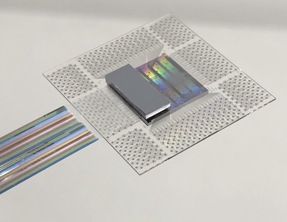
Scintil Photonics’ expertise is in the design of silicon photonics circuits and the addition of active III-V materials – for lasing, gain and modulation – to a silicon substrate.
The start-up is using its funding to move its technology from the lab to production, working with an unnamed commercial foundry. The firm is also growing its staff, from eight to a dozen by the year-end.
Menezo worked previously at CEA-Leti, a French technology research institute, where her roles included heading the silicon photonics lab and business development.
In her business role, there was interest from customers in Leti’s silicon photonics technology but, at the time, its III-V technology on silicon was not ready.
“There was an opportunity of putting III-V on silicon but quite a bit of investment was needed to make the technology more mature,” she says. “This is where you need quick money and a 100 per cent dedicated team.”
Menezo discussed the idea of a start-up with CEA-Leti and once the organisation was satisfied that the proposed venture could succeed, it enabled her to step down to focus solely on developing the technology.
In return, the organisation that oversees Leti, CEA Tech, took a share in the start-up before it sought funding. This is one of CEA Tech’s duties, says Menezo, to create jobs.
“Once the patent technology was strengthened, we went outside and looked for funding,” she says.
Technology
Scintil Photonics has both indium phosphide and silicon photonics expertise. The start-up’s plans to develop and sell fully photonic integrated circuits (PICs). The start-up’s optical component library includes lasers, modulators, waveguides, wavelength filters, and photodetectors.
“We have a fabrication process which is CMOS-friendly and which relies on existing silicon-photonics technology,” says Menezo. “We want to have silicon and III-V fabricated and we want to commercialise photonic ICs.”
Scintil’s work with a commercial foundry will take its technology to production using a standard silicon photonics process.
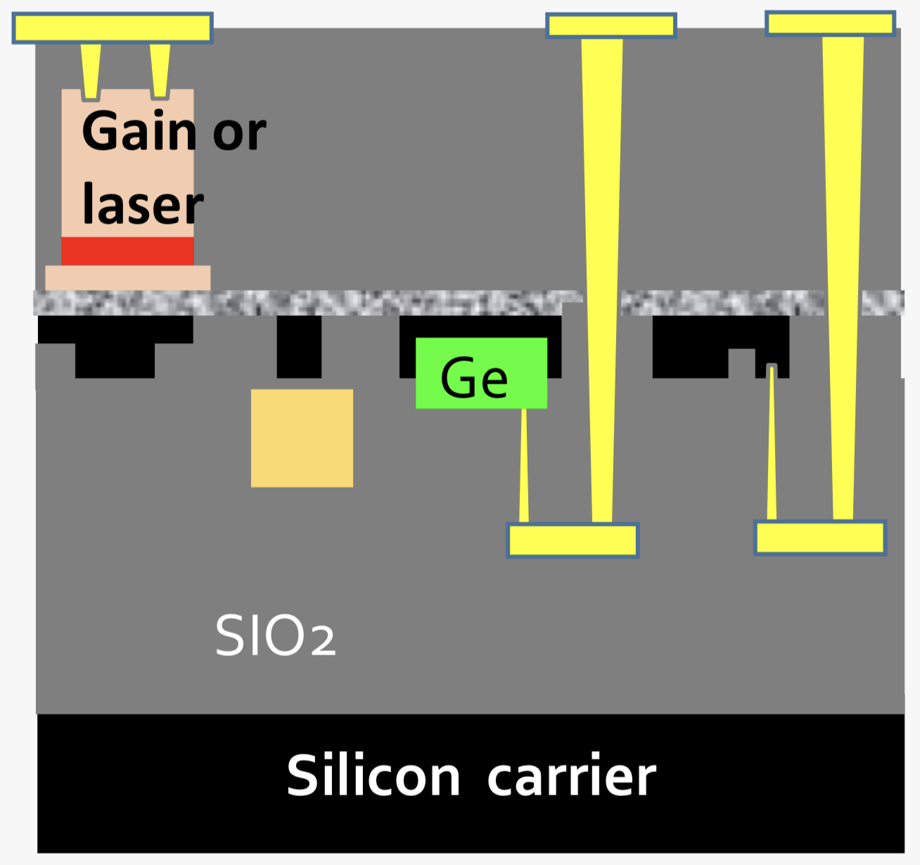
Once the silicon photonics chips are fabricated on a wafer, Scintil’s process bonds the wafer onto a silicon carrier, flips it and etches off the silicon-on-insulator (SOI) substrate.
Indium phosphide is bonded onto the exposed silicon layer before being processed to fabricate such active components as lasers, semiconductor optical amplifiers and hybrid modulators using CMOS fabrication techniques (see image).
Menezo describes the fabrication as CMOS-friendly: standard off-the-shelf processes are used while the processing of III-V is CMOS-compatible in terms of etching and electrical contacts.
Scintil’s process is also scalable, she says: new materials and functions will be added over time to the silicon photonics processes without impacting the integration of III-V materials onto the silicon.
“The more you design these devices and circuits, the more you see the design opportunities you have,” says Menezo. “This is the future if people manage to make it as a friendly as CMOS technology.”
Applications
Scintil Photonics is already working on circuit prototypes with the foundry.
The prototypes include coherent components for optical transmission and designs for 800-gigabit and 1.6-terabyte client-side interfaces. These are based on parallelising existing 400-gigabit DR4 and FR4 designs.
“For an 800-gigabit, the use of eight lanes [each lane being 100 gigabits] is indeed a good target because of [the need for] more integration,” says Menezo. “We can also scale to higher-speed lanes with our hybrid indium phosphide/ silicon photonics modulator.”
Eight-hundred gigabit modules are only needed from 2022 at the earliest.
Another application area for the technology is co-packaged optics, using optical interfaces to move data on- and off-chip.
Menezo says that the company is already thinking about the next round of funding but that it is at least two years away.