
DIMENSION tackles silicon photonics’ laser shortfall
Several companies and research institutes, part of a European project, are developing a silicon photonics process that combines on-chip electronics and lasers. Dubbed Dimension (Directly Modulated Lasers on Silicon), the silicon photonics project is part of the European Commission’s Horizon 2020 research and innovation programme.
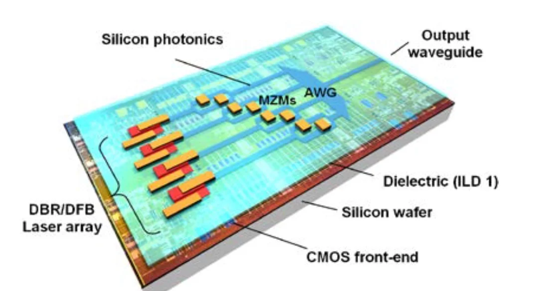 The Dimension process showing the passive photonics, dielectric material, BiCMOS circuitry, and the on-chip lasers and modulators. The indium phosphide material is shown in red. Source: Dimension.
Goal
Silicon photonics has long been seen as a technology having the potential to deliver optical devices at CMOS manufacturing costs. But silicon's key shortfall is that it does not lase. “What we see with today’s solutions is a very low-cost chip with a lot of functionality, which is a great thing, but in addition you need lasers,” says Bert Offrein, principal research staff member and manager of neuromorphic devices and systems at IBM Research, a participant in the Dimension project.
The laser accounts for a relatively large fraction of the total bill of materials of a silicon photonics chip. In turn, connecting the light source to the chip is not trivial and adds to the packaging costs. “In this project, we try to tackle this [laser] issue,” says Offrein.
The project's goal is to develop manufacturing processes that will enable the integration of photonics, including the laser, and electronics, all on one chip. “By fully integrating the laser on the chip, we massively reduce the cost and create additional functionality,” says Offrein.
“This is the true embodiment of what people first pictured as silicon photonics: the combination of optics and electronics on a single chip,” says Lars Zimmermann, team leader, silicon photonics at the Innovations for High Performance Microelectronics (IHP) research institute, another member of Dimension.
Proof-of-concept demonstrators
Dimension is a four-year project that will end in early 2020. Other project participants besides IBM Research and the IHP include ADVA Optical Networking, Opticap and the Athens Information Technology (AIT) research centre. The Dresden University of Technology is overseeing the project.
The project has set itself the goal of producing three proof-of-concept designs using the integrated silicon photonics technology.
One is a 400 Gigabit Ethernet (GbE) transmitter made up of eight 50 gigabit-per-second (Gbps) channels, each comprising a 25 gigabaud directly-modulated laser combined with 4-level pulse amplitude modulation (PAM4). Two variants are planned: a directly modulated version for the 400GbE 2km reach specification, and one with external modulation for the 400GbE 10km reach standard.
Another design is a coherent transmitter for such applications as data centre interconnect, compromising a monolithically integrated narrow-linewidth tunable laser, modulator and driver. The coherent transmitter will have a 10km target reach, will operate at 25Gbps and have a tunable narrow linewidth of under 1MHz.
The third, final demonstrator is a directly-modulated 25-gigabit non-return-to-zero laser using indium phosphide grown directly on the silicon.
By fully integrating the laser on the chip, we massively reduce the cost and create additional functionality
Process details
The silicon photonics manufacturing process involves using a silicon-on-insulator (SOI) wafer to implement the passive photonics functions and the electronics. The electronics supports high-speed analogue driver transistors and a 0.25-micron BiCMOS process used to implement the chip's control logic and control interfaces.
 Bert Offrein
The laser is constructed by first bonding a thin layer of indium phosphide. “It is structured in such a way that it [the III-V material] can be embedded completely in the whole CMOS processing,” says Offrein.
The indium phosphide layer, referred to as a III-V membrane, sits on a thin dielectric layer placed on the SOI wafer. The dielectric material is needed to protect the wafer from contamination by the III-V material and ensure that such a design could be manufactured in a BiCMOS foundry.
Once the thin indium phosphide layer is deposited, the laser can be constructed. The final stages, part of the chip-making back-end process, is the adding of metallisation layers that connect the laser and the electronics, and the circuits to the interface signals.
Growing lasers on silicon
Growing the indium phosphide layer directly on silicon, as will be done for the third demonstrator, is more exploratory. “We want to show there is a path forward on this III-V-on-silicon technology to reduce the cost further,” says Offrein.
 Lars Zimmermann
The challenge growing indium phosphide on silicon is the lattice mismatch that occurs between the two materials which leads to defects.
To tackle the issue, an approach known as confined growth is used. A small ‘seed’ is put on the silicon to act as a growth point for the indium phosphide. A small cavity is created using silica to confine the resulting growth. “The material grows in this glass cavity and the defects grow out and disappear at the edges,” says Offrein. “You then have a very high-quality III-V in this glass and this is the starting point to continue to build the quantum wells that we need.”
One challenge is enlarging the confined growth area. So far, such growth is limited to a micron whereas the length of a laser can be 500 microns typically. And once the laser is built, there remain the issues of laser reliability and temperature stability. “We will see challenges but we are not there yet,” says Offrein.
This is the true embodiment of what people first pictured as silicon photonics: the combination of optics and electronics on a single chip
Status
Dimension is tackling designs for communications but such on-chip lasers will also be useful for a range of applications such as optical sensing, says Offrein.
The project is coming to the end of its first year. Its members are creating the basic building blocks needed to realise the lasers on the silicon wafer. IBM has demonstrated the basic functionality by bonding indium phosphide to its own passive silicon photonics technology. “We have also realised the first lasers - not yet electrically pumped but optically pumped,” says Offrein. The performance of these lasers is now being characterised.
All the processes needed to pump the lasers electrically are now in place and the goal is to build complete laser structures by March 2017.
IBM is also working with IHP to see what is required to implement the technology using IHP’s own silicon photonics process. IHP is currently testing IBM’s wafers regarding any contamination issues before testing the integration process.
ADVA Optical Networking would not be on board if they were not expecting eventually to have such technology available for their products
Exploitation
The European Commission has a long history of programmes backing leading-edge research. However, Europe's track record of exploiting such research to achieve market-leading companies and products has been limited.
The European Commission staff involved in planning the Horizon 2020 projects have been far more active in ensuring that these projects are exploited, says Zimmermann. "ADVA Optical Networking would not be on board if they were not expecting eventually to have such technology available for their products," he adds.
If Dimension proves successful, IHP could make available the integrated silicon photonics process to companies to implement their opto-electronic integrated circuit designs.
IBM, while no longer a semiconductor manufacturer, would also be keen for the technology to be transferred to large foundries such as STMicroelectronics and GlobalFoundries. “That way we could purchase the technology and apply it in our own systems,” says Offrein.
Article amended on Nov 29th. Added details about the proof-of-concept demonstrators.
IBM demos a 100 Gigabit silicon photonics transceiver
“It is a demonstration vehicle illustrating the complex design capabilities of the technology and the functionality of the optical and electrical components,” says Will Green, manager of IBM’s silicon integrated nano-photonics group.
 Will Green
IBM has been developing silicon photonics technology for over a decade, starting with building-block optical functions based on silicon, to its current monolithic system-on-chip technology that includes design tools, testing and packaging technologies.
Now this technology is nearing commercialisation.
“We do plan to have the technology available for use within IBM’s systems but also within the larger market; large-volume applications such as the data centre and hyper-scale data centres in particular,” says Green.
IBM is already working with companies developing their own optical component designs using its technology and design tools. “These are tools that circuit designers are familiar with, such that they do not need to have an in-depth knowledge of photonics in order to build, for example, an optical transceiver,” says Green.
We do plan to have the technology available for use within IBM’s systems but also within the larger market
100 gig demonstrator
IBM refers to its silicon photonics technology as CMOS-integrated nano-photonics. CMOS-integrated refers to the technology’s monolithic nature that combines CMOS electronics with photonics on one substrate. Nano-photonics highlights the dimensions of the feature sizes used.
IBM is rare among the silicon photonics community in combining electronics and photonics on one chip; other players implement photonics and electronics on separate dies before combining the two. What is not included is the laser which is externally attached using fibre.
The platform supports 25 gigabit speeds as well as wavelength division multiplexing. Originally, IBM started with 90 nm CMOS using bulk silicon before transferring to a silicon-on-insulator (SOI) substrate. An SOI wafer is ideal for creating optical waveguides that confine light using the large refractive index difference between silicon and silicon dioxide. However, to make the electrical devices run at 25 gigabit, the resulting transistor gate length ended up being closer to a 65 nm CMOS process.
 Source: IBM Corporation.
IBM's optical waveguides are sub-micron, having dimensions of a few hundred nanometers. This is the middle ground, says Green, trading off the density of smaller-dimensioned waveguides with larger, micron-plus ones that deliver low propagation loss.
Also used are sub-wavelength optical 'metamaterial' structures that transition between the refractive index of the fibre and that of the optical waveguide to achieve a good match between the two. “These very tiny sub-wavelength structures are made using lithography near the limits of what is available,” says Green. “We are engineering the optical properties of the waveguide in order to achieve a low insertion loss when bringing the fibre onto the chip.” The single mode fibre to the chip is attached using passive alignment.
The 100 gigabit transceiver demonstrator uses four 25 gigabit coarse wavelengths around 1310 nm. The technology is suited to implement the CWDM4 MSA.
The whole technology is available to be commercialised by any chip manufacturer
“We are working with four wavelengths today but in the same way as telecom uses many wavelengths, we can follow a similar path,” says Green.
The chip design features transmitter electronics - a series of amplifiers that boost the voltage to drive the Mach-Zehnder Interferometer modulators - and a multiplexer to combine the four wavelengths onto the fibre while the receiver circuitry includes a demultiplexer, four photo-detectors and trans-impedance amplifiers and limiting amplifiers, says Green. What is lacking to make the 100 gigabit transceiver functional is a micro-controller, feedback loops to control the temperature of key circuits, and the circuitry to interface to standard electrical input/ output.
Green highlights how the bill of materials of a chip is only a fraction of the total cost since assembly and testing must also be included.
“We reduce the cost of assembly through automated passive optical alignment and the introduction of custom structures onto the wafer,” he says. “We believe we can make an impact on the cost structure of the optical transceiver and where this technology needs to be to access the data centre.” IBM has also developed a way to test the transceiver chips at the wafer level.
Green admits that its CMOS-integrated nanophotonics process will not scale beyond 25 gigabit as the 90-65 nm CMOS is not able to implement faster serial rates. But IBM has already shown an optical implementation of the PAM-4 modulation scheme that doubles a link's rate to 50 gigabit.
Meanwhile, IBM’s process design kit (PDK) is already with customers. A PDK includes documents and data files that describe the fabrication process and enable a user to complete a design. A PDK includes a fab’s process parameters, mask layout instructions, and the library of silicon photonics components; grating couplers, waveguides, modulators and the like [1].
“They [customers] have used the design kit provided by IBM but have built their own designs,” says Green. “And now they are testing hardware.”
IBM is keen that its silicon photonics technology will be licensed and used by circuit design houses. "Houses that bring their own IP [intellectual property], use the enablement tools and manufacture at a site that is licensing the technology from IBM,” says Green. "The whole technology is available to be commercialised by any chip manufacturer.”
Reference
[1] Silicon Photonics Design: From Devices to Systems, Lukas Chrostowski and Michael Hochberg, Cambridge University Press, 2015. Click here
Q&A with photonics pioneer, Richard Soref - Part 1
Richard Soref has spent over 50 years researching photonics, contributing groundbreaking work in the areas of liquid crystals, silicon photonics and the broader topic of mid-infrared wavelengths and Group IV photonics. For 27 years he was employed at the Air Force Research Laboratory. He has also worked at the Sperry Research Center, the MIT Lincoln Laboratory, and is now a research professor at the University of Massachusetts in Boston.
In part 1 of a two-part interview with Gazettabyte, he details his research interests, explains what is meant by Group IV photonics, and discusses why photonics has not matched the semiconductor industry in terms of integration, and how that could change.
Optics is a seemingly small subset of physics but really optics is a huge field with a deep, variegated nature waiting to be discovered
Richard Soref
Q: Having gained your Ph.D. in 1963, you have spent your career in what you call the science of light. What is it about photonics that you find so captivating?
RS: I’ve been drawn to its diversity and classical beauty. Photonics used to be called optics until it was re-labelled by the OSA. Optics is a seemingly small subset of physics but really optics is a huge field with a deep, variegated nature waiting to be discovered. To make progress, you need multiple disciplines, and I’ve always been captivated by the materials science aspect that opens the door to new physics and new devices.
Can you outline your career and how you ended up as a research professor at the University of Massachusetts at Boston?
RS: A general outline is that I chose employers who would encourage exploration of new avenues, would give me freedom to fly or fall – and both are built into research. Basic research is where my talents and passion align. And it helps to be obsessive.
In the early years, I worked mostly alone. Then the pleasures of collaboration became important, and for decades I have been fortunate to have outstanding research partners who did heavy lifting of things like quantum mechanics and electromagnetic modelling.
At Lincoln Lab, I continued the nonlinear optical studies that I began during my Stanford Ph.D. work. Sperry Research was an excellent environment until it fell victim to the corporate research shutdown contagion. Ironically or prophetically, impurity-doped silicon infrared sensors were an early focus at Sperry.
Lithium niobate sparked my 40-year interest in electro-optics: Pockels [effect], Kerr [electro-optic effect], Franz-Keldysh [effect] and more. My extensive work on liquid crystals gained a lot of traction, and at an Information Display show I met scientists from South Korea who told me that my early papers helped them with their commercial flat-panel TV products. It was fulfilling to hear that.
Apart from some governmental distractions, the Air Force Research Laboratory (AFRL) years were a happy time and I welcomed the support of the Air Force Office of Scientific Research (AFOSR); the AFOSR is a national treasure.
Fibre-optic telecom emerged in 1985 when I was at AFRL. The fibres needed semiconductor assistance, I felt. That’s when the new silicon insights came to me. I’m glad that I was able in 1989 to identify silicon-on-insulator (SOI) as the primary waveguided-network platform, and I’m gratified that brilliant and innovative research groups around the world entered this field early on. They strived successfully to perfect this technology. To do my part, I tried to surround the problem in a 1985-2015 series of papers, among them my 1991 silicon-germanium-tin (SiGeSn) direct-gap prediction and my 1992 opto-electronic integrated circuit (OEIC) proposal. My most-cited work is a 1987 paper on free-carrier electro-optics.
Summarising, I had two visions at AFRL: Group IV photonics and long-wave integrated optoelectronics, where long wave denotes anything from two to 200 microns, although the mid-infrared wavelengths are key because of their room temperature possibilities. Perhaps there is a third vision: the multi-technology 3D chip on which seven technologies including bio-chemical could be combined.
Sadly those creative years drew to a close when the Massachusetts laboratory was shut down by the Air Force and the party moved to Wright Patterson AFB in Ohio. At that point, I joined the University of Massachusetts in Boston to stay near family and to keep the technical flame alive in research. I’m still collaborating with wonderful people, most of them young.
Can you provide rigour regarding some definitions? Starting with silicon photonics, silicon mid-infrared optics and Group IV photonics, can you define each and do you have a preference for a particular term?
RS: The silicon-photonics term is strongly entrenched in the global community. The phrase includes on-chip germanium photo-detectors and presumably germanium lasers. Nevertheless, I think this term is a bit narrow or misleading about the silicon-germanium-tin materials (SiGeSn) that likely will be used in the monolithic silicon chip of the future.
I am in the minority when I say that I prefer the wider term Group IV photonics (GFP) which takes into account those three-part alloys as well as diamond and graphene. This GFP term was coined in 2003 in my office at Hanscom when Greg Sun and I were dreaming constructively about a new, dedicated IEEE conference, the international meeting I co-founded in 2004.
In the coming years, the purely photonic integrated circuit, the PIC chip, will evolve, after money is spent, into the opto-electronic chip, and the transistors will be CMOS or BiCMOS or heterojunction bipolar
What about the OEIC, how does it differ from silicon photonics? And lastly, nano-photonics, how does it compare to silicon photonics?
RS: The opto-electronic integrated circuit describes the synergistic marriage of nano-photonics and nano-electronics on the same silicon chip. Others have called this an electronic-photonic integrated circuit or EPIC. In essence, the OEIC is a transistorised photonic chip containing electronic intelligence, signal processing, computation, electrical control of active photonic devices, and perhaps RF wireless transceiving capability, which I strongly advocate.
In the coming years, the purely photonic integrated circuit, the PIC chip, will evolve, after money is spent, into the opto-electronic chip, and the transistors will be CMOS or BiCMOS or heterojunction bipolar. These possibilities illustrate the diversity of GFP.
As for nano-photonics, it is a subset of silicon photonics populated by wave-guided components whose smallest cross-section dimension is 15 to 30 percent of the free-space wavelength. Photonics, like electronics, started as micro and shrank to nano. The term nano means nanometer-scale and applies also to quantum-dot diameter, quantum-well layer thickness and photonic-crystal air hole diameter.
In over half a century, electronics has undergone an extraordinary transformation from simple integrated circuits to profoundly complex ones. Yet while integrated optics was spoken of as early as 1969 in the Bell Labs paper by Stuart Miller, integration has been far more modest. Why?
RS: The main roadblock has been the lack of compelling applications for medium scale and large scale photonic integration. Perhaps this was a lack of vision or a lack of market to drive the integration research.
Another inhibiting factor is the large expense, the cost-per-run of making a photonic integrated circuit, although the OPSIS user foundry [before it closed] and other user facilities have mitigated entry costs to some extent. Additional factors are the area-footprint and volume of the photonic building blocks. The photonic device size is generally larger, or much larger, than the size of the modern individual transistor.
Is this about to change?
RS: To some degree, yes. People are packing photonic components together in a circuit but there are limits on how closely this can be done. These constraints lead me to wonder whether photonic integration will follow the same historical path as micro- and nano-electronics, the same developmental story. Will there be a Moore’s law for photonics with PIC packing density doubling every 18 months? The billion-photonic circuit is not on the cards, so I doubt that the law will hold.
The diffraction limit of optics and the single-mode criteria set lower limits on photonic size, although plasmonic devices go below those dimensional limits and are compatible with photonics.
I see glimmers today of where LSI can make a difference. A near-term use is a 128x128 array of electro-optical phase shifters for optical beam steering. More speculatively, we have electro-optical logic arrays, spectrometers on-chip, optical neural networks, dense wavelength-division multiplexers and demultiplexers, quantum processors, and optical computers using dense nano-LED arrays.
The government has deeper pockets than industry for sustained R&D efforts
What are the major challenges today making optical devices using a CMOS fabrication process?
RS: A partially-met challenge is to actualise a stable and reliable process in a 130nm or 65nm CMOS node for manufacturing the active and passive photonic parts of the on-chip network. We need process procedures for principal components which are recipes defined with a new design library. Whether to standardise photonics is an open question. When and where to place transistor circuits on-chip is a challenge. Putting transistors on a separate chip is a near-term alternative.
It takes art as well as science to determine the opto-electronic layering and to decide whether the available processing temperatures necessitate fabrication at the front end or back end of the overall process.
I believe that a manufacturing initiative is an essential next step for GFP to convince friends and skeptics alike of the long-term commercial and military value of GFP offered in new generations of energy-efficient ultra-performance chipsets. The government has deeper pockets than industry for sustained R&D efforts, so I believe that the Department of Defense can be the force driving GFP expansion into higher realms at very low costs per chip.
That’s why I welcome the new 5-year Integrated Photonics Institute project as part of the National Network for Manufacturing Innovation, funded by the RAMI bill [Revitalize American Manufacturing and Innovation Act]. It is a bill that would train the workforce, while public-private partnerships will transform research into products and will deploy infrastructure that supports US-enterprise competitiveness.
For the second part, click here