
By invitation: Professor Roel Baets on Silicon Photonics 4.0

Roel Baets, Emeritus Professor at Ghent University and former Group Leader at imec gave a plenary talk on ‘Silicon Photonics 4.0’ at the recent ECOC conference. “It will be important for silicon photonics to make use of smart and agile manufacturing, a notion associated with Industry 4.0,” said Professor Baets, explaining the title.
In a guest piece, he explains his thoughts and discusses what he saw at ECOC. He also has a request.
One of the things I discussed in my ECOC plenary talk was the large gap between research and product development for new applications of photonic integrated circuits (PICs) on the one hand, and product sales and new industrial process flows on the other.
Among many reasons for this gap, one stands out: the major barriers that fabless start-ups face when developing a product based on a still immature industrial supply chain.
This often implies that part of the start-up’s non-recurring engineering (NRE) budget needs to be spent on co-investment in a new process flow by a technology provider, which can easily be too expensive for a start-up. The growing diversity in materials added to silicon photonics process flows to meet the needs of new applications is a major compounding factor in this context.
I showed a slide that listed the companies that I am aware of that sell non-transceiver products based on PICs (silicon or other). I try to keep this list up to date with my Ghent University colleague, Prof. Wim Bogaerts, chair of ePIXfab. The slide showed only seven companies, while there are probably between 100 and 200 companies around the world that develop such products.
These companies are Genalyte (biosensors for diagnostics), Anello (optical gyroscope), Sentea and PhotonFirst (fibre Bragg grating readout), Quix (quantum processor), Thorlabs (>100GHz opto-electronic converter) and iPronics (originally a programmable photonic processor company now focussing on optical switching). These companies will likely sell only in modest numbers, but at least they sell a product.
After my talk, I eagerly went to the ECOC exhibition in the hope of spotting additional companies. I found two that I could add to the list: Chilas (tunable low-linewidth lasers) and SuperLight Photonics (supercontinuum lasers).
A few weeks later, I discovered yet another fledgling company ready to sell: hQphotonics (ultra-low-noise microwave oscillators). So the list is double-digit now! Perhaps this is an important milestone towards Silicon Photonics 4.0.
Interestingly, four of those ten companies use Silicon-on-Insulator (SOI) technology, four use silicon nitride PICs, one uses InP, and one uses thin-film Lithium Niobate (TFLN).
Undoubtedly, the list is incomplete. There may be other companies with a product (not just a prototype or a demo kit or a technology service) that we do not know.
So let me make a call to contact me if you know of any company not on the list of ten that sells a non-transceiver product based on PICs.
roel.baets@ugent.be

Silicon photonics' second wave
Two concentric circles drawn in chalk are shown on-screen. So Professor Roel Baets open his plenary talk at the European Conference on Integrated Optics (ECIO) 2020, asking the online audience what is being shown.

Professor Roel Baets
Suggestions come flooding in: the cross-section of an optical fibre, a silicon wafer, a ring resonator optical component and - the correct answer - a doughnut.
The image is from the front cover of Doughnut Economics: Seven Ways to Think Like a 21st-Century Economist by Kate Raworth, a UK professor of economics.
The author discusses how continual economic growth is out of kilter with the planet’s well-being and details alternative approaches. The “doughnut” represents a sweet-spot region ensuring sustainable growth.
Baets applied the book’s thinking to his plenary talk on the topic of silicon photonics research.
Research perspective
Baets’ research work focusses on the use of silicon photonics for applications other than telecom and datacom.
High-speed transceivers for telecom and datacom continue to drive silicon photonics, creating mature platforms and funding the technology’s development.
The two industries will also continue to drive silicon photonics for the coming decade but the picture is set to change. “There is huge potential for other markets; sensing, life sciences and medical being some of them,” he says.
Baets is director of the multidisciplinary Centre for Nano- and Biophotonics at Ghent University in Belgium. His research group comprises 90 staff, split between Ghent University and imec, the renowned R&D centre. “We are sort of a hybrid unit, part university and part imec,” he says.
His focus on the next wave of silicon photonics is partly due to a long-standing interest in biomedical engineering and because high-speed transceiver research is now mainstream.
“I have a big appetite to do something less evolutionary and more groundbreaking,” he says.
Applying the technology to do something helpful appeals to him: “Diagnosing diseases or for therapy of diseases, I feel that is more relevant.”
Background
Baets received the 2020 John Tyndall Award from The Optical Society (OSA) and the IEEE Photonics Society. The award is for his “seminal research in silicon photonics and for driving the foundry model in this field.”
Baets read electrical engineering at Ghent University where he also earned a masters degree. He gained a second masters at Stanford University in California.
“It sounds redundant but I had the privilege of doing a lot of things in terms of subjects that I hadn’t been able to do at Ghent so it was wonderful,” says Baets.
It was at Stanford that Baets pursued his interest in biomedical engineering. He also ‘fell in love’ with photonics after he met and worked with Joseph Goodman, whom he describes as the father of Fourier optics and statistical optics.
That set the course of his photonics research, while his interest in biomedical engineering remained. “And it [biomedical engineering] has popped up in recent years in combination with photonics,” he says.
Foundry model
Baets compares the progress of silicon photonics with that of the chip industry several decades ago.
In the 1970s, universities undertaking integrated circuit research had clean rooms but the growing sophistication of chip-making meant it became too costly.
“Universities and research groups had to give up having their own fabrication facilities for research,” he says.
The same happened within the chip industry, with few chip firms able to afford clean rooms resulting in the advent of foundries.
Even the semiconductor titan Intel, which built its fortune by leading the chip industry in CMOS process technology, is now considering foundries to make its chips.
A similar model is now playing out with integrated photonics.
>
“I believe the field of silicon photonics is at a pivotal point of change and acceleration.”
“The microelectronics fab is an extremely expensive infrastructure,” says Baets. “Maintaining the process flow for certain platforms that enable you to combine [optical] functions on-chip takes quite a bit of diligence and therefore cost.”
This is why creating ‘open’ mechanisms whereby interested parties can gain access to such technology is so important.
“Even if you don’t have a fab in your backyard, there are places you can go to,” says Baets. “That was the essence behind starting ePIXfab.”
Baets helped found ePIXfab, the first global multi-project wafer service for silicon photonics, in 2006.
The idea of multi-project wafers is to aggregate photonic designs from many different users into one mask set before passing a wafer run through a fab. “Multi-project wafers is a cost-sharing process that is well established in electronics,” he says.
Platforms
The Kate Raworth book on sustainable growth was an eye-opener to many people, says Baets, given the topic was addressed by an economist rather than a climate-change scientist.
“Growth is important but there are other dimensions, and you need to find a sweet spot,” he says. “I couldn’t resist using this for my ECIO talk as a metaphor for the field of silicon photonics.”
Silicon photonics is at a turning point, he says, and it will be interesting to see how the field develops over the next five to ten years in terms of finding a way to create mature platforms serving different applications and markets.
The term platform refers to the entire chain of processes that happen in a microelectronics fab, starting with plain wafers and ending with diced chips.
When Baets talks about mature platforms he is referring to a standardised process flow where the basic components are well defined and where a user has some freedom in how the optical functions are connected. It should also be “open access”, similar to CMOS chip foundries.
The technology used for chip-making - the wafer-level processes and the infrastructure - is hugely expensive yet what it produces - the chips - are ‘insanely cheap’, says Baets
“Because of these special boundary conditions, you have to be careful in the research directions you choose,” he says. ”It doesn’t make sense to embark in a direction where it is hard to imagine how it would fit into a sustainable platform.“
This is the essence of his plenary talk.
For example, several places around the world have created a process flow that combines silicon nitride optical waveguides with standard silicon ones. This has only happened in the last couple of years.
“It is a beautiful example of how you can extend the richness of a platform to another level, thereby serving many new applications and customers,” he says.
Meanwhile, a current focus of academic research concerns ways to add III-V lasers to the silica substrate, what he describes as the Holy Grail of silicon photonics.
Baets stresses that there is huge potential for many different applications in the coming years but that it will only happen if real-world products can be made in places that have mature, open-access platforms.
“This is not entirely trivial as it is expensive to establish such platforms,” he says.
There is also this dream of creating a unified platform that can do everything. But Baets says such a generic platform is unrealistic given the overall range of wavelengths used, for datacom, telecom and the longer wavelengths of infra-red.
“You cannot expect one platform to serve all of these,” says Baets. ”But, equally, if there is too much fragmentation, things will not turn out well,” he says.
Baets is aware of at least 20-30 start-up companies developing silicon photonics products, not for datacom or telecom.
In his plenary talk he listed such applications as neuromorphic computing, quantum computing, virtual reality – augmented reality, environmental sensing such as for gas using mid-infrared, critical infrastructure monitoring, and a variery of medical applications such as biosensors, cardiovascular monitoring, glucose monitoring neurophotonics and optical coherence tomography.
Not all these players will be successful but he does expect silicon photonics chips to be made in volumes that will eclipse telecom and datacom in the next five years or so.
But that brings us back to the issue of platforms. “Can they [designers] do things with the existing platforms or do they need a platform that goes a step further - or three steps further?” he says. “And then that question of a unified platform comes up again.”
Training
Baets is dedicating part of his time to address the issue of training in silicon photonics.
“There is a shortage of people with the skills to do silicon photonics,” he says.
Silicon foundries are full of people that understand electronics devices and there is a need for people that understand photonic devices, which are different.
People are also needed with application skills.
“If you think of medical devices, there is a vast distance between expertise in medical-device companies and expertise in the field of silicon photonics,” says Baets. “So there is a need for a lot of bridging work to make people aware of the potential of photonics in general and silicon photonics in particular.”
This is a role ePIXfab has embraced with training activities to address this need.
Research goals
What would Baets like to witness given another decade of uninterrupted research work?
“It is all about impact,” he says. “You would want to see research work turned into something that, at the end of the day, helps people.”
He has great respect for curiosity-driven research. “Curiosity-driven research is like art,” he says. “It is something that is beautiful if done by people with the right skills and is something that society can afford.”
But he is less attracted to conceptual beauty and more to things that prove helpful: “This whole field is about things that help people, whether that is the internet or a medical device.”
Meanwhile, there is COVID-19 to contend with.
As we complete the interview, Baets has a follow-on online meeting with his students.
And the previous evening he attended his first live concert since the start of the COVID-19 lockdown, given by Belgium jazz pianist, Jef Neve. “It was a privilege and it was very enjoyable,” he says.
Classical music is a passion of Baets and in his youth, he played the piano.
“The number of times I now touch the piano is limited but I have some ambition to take it up again,” he says.
Further Information:
Kim Roberts, 2019 John Tyndall Award winner, click here

X-Celeprint brings printing technology to silicon photonics
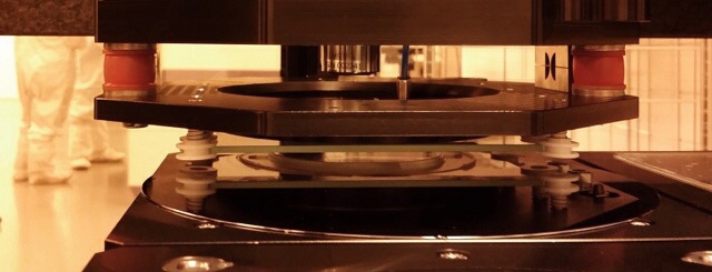 X-Celeprint's micro transfer printing technology. Source: X-Celeprint
- X-Celeprint has a printing process that places individual 'chiplets' of III-V material onto silicon
- The micro transfer printing technique can be used to make silicon photonics circuits
- X-Celeprint will work with silicon photonics companies interested in licensing its technology
A key challenge facing silicon photonics players is creating a light source. Silicon does not lase so a III-V material is needed to form the laser.
One approach is to attach a tiny module holding the laser to the silicon photonics design. This is what the likes of Cisco Systems, Luxtera, Mellanox Technologies and IBM are doing: adding an external laser to the otherwise monolithic silicon photonics circuit.
An alternative technique is to bond the III-V material to the silicon and using photolithography and etching to construct the silicon photonics device. The attraction of III-V bonding is that the technique can be used to also make the modulators and photo-detectors. Known as heterogeneous integration, this approach is being used by companies such as Aurrion, Intel and Skorpios Technologies.
"Bonding is an elegant solution," says Roel Baets, a professor at the Photonics Research Group at Ghent University. "You can make the light source at the wafer scale and have a single chip solution that looks like a monolithic chip, including the light source."
Think of printing as pick-and-place in a massively parallel fashion. Instead of ink, we are picking up and printing arrays of high-performance semiconductors.
Bonding III-V material to silicon is itself non-trivial. First, silicon wafers are either 200mm or 300mm (8 or 12 inch) while III-V indium phosphide wafers are typically 50mm (2 inch). Indium phosphide wafers are also expensive, simply etching away the majority of the wafer to leave small islands of wanted material is hugely wasteful.
"There is only going to be a laser here or there, with a fill factor - an area coverage - of some one percent," says Baets. "You are throwing away a lot of III-V."
Equally, cutting up the III-V wafer into small slivers for bonding is complicated as it requires precision placement; a process difficult to automate to achieve high-yield circuits. This is the challenge the heterogeneous integration companies have set themselves.
It is a market opportunity identified by start-up X-Celeprint. It has a process that places individual 'chiplets' of III-V material onto silicon by the thousands.
X-Celeprint uses a micro transfer printing to place the chiplets onto silicon. "Think of printing as pick-and-place in a massively parallel fashion," says Kyle Benkendorfer, CEO of X-Celeprint. "Instead of ink, we are picking up and printing arrays of high-performance semiconductors."
Micro transfer printing is already used commercially to make high concentration solar cells, and it is being evaluated to place thin lasers on read/ write heads in disc drives. "We can print live devices or a slab of material on any substrate as long as it is flat," says Benkendorfer.
One benefit of the technique is that the thin III-V material is removed from the indium phosphide wafer but the underlying substrate is retained and can be recycled. For wafer-to-wafer bonding, in contrast, the substrate must be ground back. "This is several hundred microns of [substrate] material," says Benkendorfer. "With our process you can reprocess the wafer and regrow it, saving some $3,000."
The printing process also lends itself to automation. "We can very efficiently place active die of highly expensive compound material at the point of use, where it can then be converted into a device," he says.
X-Celeprint wants to work with silicon photonics companies interested in licensing its printing technology. Developing the process with a particular silicon photonics vendor takes time. Each application requires tailoring and it can take up to two years to make, test and scale up production, says the start-up.
"We recognise that silicon photonics as a large market is out there, no question," says Benkendorfer. "But the development time to get any significant market is going to be a while."