
New MSA to enable four-lambda 400-gigabit modules
A new 100-gigabit single-wavelength multi-source agreement (MSA) has been created to provide the industry with 2km and 10km 100-gigabit and 400-gigabit four-wavelength interfaces.
 Mark NowellThe MSA is backed by 22 founding companies including Microsoft, Alibaba and Cisco Systems.
The initiative started work two months ago and a draft specification is expected before the year end.
“Twenty-two companies is a very large MSA at this stage, which shows the strong interest in this technology,” says Mark Nowell, distinguished engineer, data centre switching at Cisco Systems and co-chair of the 100G Lambda MSA. “It is clear this is going to be the workhorse technology for the industry for quite a while.”
Phased approach
The 100G Lambda MSA is a phased project. In the first phase, three single-mode fibre optical interfaces will be specified: a 100-gigabit 2km link (100G-FR), a 100-gigabit 10km link (100G-LR), and a 2km 400-gigabit coarse wavelength-division multiplexed (CWDM) design, known as the 400G-FR4. A 10km version of the 400-gigabit CWDM design (400G-LR4) will be developed in the second phase.
For the specifications, the MSA will use work already done by the IEEE that has defined two 100-gigabit-per-wavelength specifications. The IEEE 802.3bs 400 Gigabit Ethernet Task Force has defined a 400-gigabit parallel fibre interface over 500m, referred to as DR4 (400GBASE-DR4). The second, the work of the IEEE 802.3cd 50, 100 and 200 Gigabit Ethernet Task Force, defines the DR (100GBASE-DR), a 100-gigabit single lane specification for 500m.
Twenty-two companies is a very large MSA at this stage, which shows the strong interest in this technology
“The data rate is known, the type of forward-error correction is the same, and we have a starting point with the DR specs - we know what their transmit levels and receive levels are,” says Nowell. The new MSA will need to contend with the extra signal loss to extend the link distances to 2km and 10km.
With the 2km 400G-FR4 specification, not only does the design involve longer distances but also loss introduced using an optical multiplexer and demultiplexer to combine and separate the four wavelengths transmitted over the single-mode fibre.
“It is really a technical problem, one of partitioning the specifications to account for the extra loss of the link channel,” says Nowell.
One way to address the additional loss is to increase the transmitter’s laser power but that raises the design’s overall power consumption. And since the industry continually improves receiver performance - its sensitivity - over time, any decision to raise the transmitter power needs careful consideration. “There is always a trade off,” says Nowell. “You don't want to put too much power on the transmitter because you can’t change that specification.”
The MSA will need to decide whether the transmitter power is increased or is kept the same and then the focus will turn to the receiver technology. “This is where a lot of the hard work occurs,” he says.
Origins
The MSA came about after the IEEE 802.3bs 400 Gigabit Ethernet Task Force defined 2km (400GBASE-FR8) and 10km (400GBASE-LR8 interfaces based on eight 50 gigabit-per-second wavelengths. “There was concern or skepticism that some of the IEEE specification for 2km and 10km at 400 gigabits were going to be the lowest cost,” says Nowell. Issues include fitting eight wavelengths within the modules as well as the cost of eight lasers. Many of the large cloud players wanted a four-wavelength solution and they wanted it specified.
The debate then turned to whether to get the work done within the IEEE or to create an MSA. Given the urgency that the industry wanted such a specification, there was a concern that it might take too long to get the project started and completed using an IEEE framework, so the decision was made to create the MSA.
“The aim is to write these specifications as quickly as we can but with the assumption that the IEEE will pick up the challenge of taking on the same scope,” says Nowell. “So the specs are planned to be written following IEEE methodology.” That way, when the IEEE does address this, it will have work it can reference.
“We are not saying that the MSA spec will go into the IEEE,” says Nowell. “We are just making it so that the IEEE, if they chose, can quickly and easily have a very good starting point.”
Form factors
The MSA specification does not dictate the modules to be used when implementing the 100-gigabit-based wavelength designs. An obvious candidate for the single-wavelength 2km and 10km designs is the SFP-DD. And Nowell says the OSFP and the QSFP-DD pluggable optical modules as well as COBO, the embedded optics specification, will be used to implement 400G-FR4. “From Cisco’s point of view, we believe the QSFP-DD is where it is going to get most of its traction,” says Nowell, who is also co-chair of the QSFP-DD MSA.
Nowell points out that the industry knows how to build systems using the QSFP form factors: how the systems are cooled and how the high-speed tracks are laid down. The development of the QSFP-DD enables the industry to reuse this experience to build new high-density systems.
“And the backward compatibility of the QSFP-DD is massively important,” he says. A QSFP-DD port also supports the QSFP28 and QSFP modules. Nowell says there are customers that buy the latest 100-gigabit switches but use lower-speed 40-gigabit QSFP modules until their network needs 100 gigabits. “We have customers that say they want to do the same thing with 100 and 400 gigabits,” says Nowell. “That is what motivated us to solve that backward-compatibility problem.”
Roadmap
A draft specification of the phase one work will be published by the 22 founding companies this year. Once published, other companies - ‘contributors’ - will join and add their comments and requirements. Further refinement will then be needed before the final MSA specification, expected by mid-2018. Meanwhile, the development of the 10km 400G-LR4 interface will start during the first half of 2018.
The MSA work is focussed on developing the 100-gigabit and 400-gigabit specifications. But Nowell says the work will help set up what comes next after 400 gigabits, whether that is 800 gigabits, one terabit or whatever.
“Once a technology gets widely adopted, you get a lot of maturity around it,” he says. “A lot of knowledge about where and how it can be extended.”
There are now optical module makers building eight-wavelength optical solutions while in the IEEE there are developments to start 100-gigabit electrical interfaces, he says: “There are a lot of pieces out there that are lining up.”
The 22 founding members of the 100G Lambda MSA Group are: Alibaba, Arista Networks, Broadcom, Ciena, Cisco, Finisar, Foxconn Interconnect Technology, Inphi, Intel, Juniper Networks, Lumentum, Luxtera, MACOM, MaxLinear, Microsoft, Molex, NeoPhotonics, Nokia, Oclaro, Semtech, Source Photonics and Sumitomo Electric.
Inphi unveils a second 400G PAM-4 IC family
Inphi has announced the Vega family of 4-level, pulse-amplitude modulation (PAM-4) chips for 400-gigabit interfaces.
 The 16nm CMOS Vega IC family is designed for enterprise line cards and is Inphi’s second family of 400-gigabit chips that support eight lanes of 50-gigabit PAM-4.
Its first 8x50-gigabit family, dubbed Polaris, is used within 400-gigabit optical modules and was announced at the OFC show held in Los Angeles in March.
“Polaris is a stripped-down low-power DSP targeted at optical module applications,” says Siddharth Sheth, senior vice president, networking interconnect at Inphi (pictured). “Vega, also eight by 50-gigabits, is aimed at enterprise OEMs for their line-card retimer and gearbox applications.”
A third Inphi 400-gigabit chip family, supporting four channels of 100-gigabit PAM-4 within optical modules, will be announced later this year or early next year.
400G PAM-4 drivers
Inphi’s PAM-4 chips have been developed in anticipation of the emergence of next-generation 6.4-terabit and 12.8-terabit switch silicon and accompanying 400-gigabit optical modules such as the OSFP and QSFP-DD form factors.
Sheth highlights Broadcom’s Tomahawk-III, start-up Innovium’s Teralynx and Mellanox’s Spectrum-2 switch silicon. All have 50-gigabit PAM-4 interfaces implemented using 25-gigabaud signalling and PAM-4 modulation.
“What is required is that such switch silicon is available and mature in order for us to deploy our PAM-4 products,” says Sheth. “Everything we are seeing suggests that the switch silicon will be available by the end of this year and will probably go into production by the end of next year,” says Sheth.
Several optical module makers are starting to build 8x50-gigabit OSFP and QSFP-DD products
The other key product that needs to be available is the 400-gigabit optical modules. The industry is pursuing two main form factors: the OSFP and the QSFP-DD. Google and switch maker Arista Networks are proponents of the OSFP form factor while the likes of Amazon, Facebook and Cisco back the QSFP-DD. Google has said that it will initially use an 8x50-gigabit module implementation for 400 gigabit. Such a solution uses existing, mature 25-gigabit optics and will be available sooner than the more demanding 4x100-gigabit design that Amazon, Facebook and Cisco are waiting for. The 4x100 gigabit design requires 50Gbaud optics and a 50Gbaud PAM-4 chip.
Inphi says several optical module makers are starting to build 8x50-gigabit OSFP and QSFP-DD products and that its Polaris and Vega family of chips anticipate such deployments.
“We expect 100-gigabit optics to be available sometime around mid-2018 and our next-generation 100-gigabit PAM-4 will be available in the early part of next year,” says Sheth.
Accordingly, the combination of the switch silicon and optics means that the complete ecosystem will already exist next year, he says
Vega
The Polaris chip, used within an optical module, equalises the optical non-linearities of the incoming 50-gigabit PAM-4 signals. The optical signal is created using 25-gigabit lasers that are modulated using a PAM-4 signal that encodes two bits per signal. “When you run PAM-4 over fibre - whether multi-mode or single mode - the signal undergoes a lot of distortion,” says Sheth. “You need the DSP to clean up that distortion.”
The Vega chip, in contrast, sits on enterprise line cards and adds digital functionality that is not supported by the switch silicon. Most enterprise boxes support legacy data rates such as 10 gigabit and 1 gigabit. The Vega chip supports such legacy rates as well as 25, 50, 100, 200 and 400 gigabit, says Sheth.
The Vega chip can add forward-error correction to a data stream and decode it. As well as FEC, the chip also has physical coding sublayer (PCS) functionality. “Every time you need to encode a signal with FEC or decode it, you need to unravel the Ethernet data stream and then reassemble it,” says Sheth.
Also on-chip is a crossbar that can switch any lane to any other lane before feeding the data to the switch silicon.
Sheth stresses that not all switch chip applications need the Vega. For large-scale data centre applications that use stripped-down systems, the optical module would feed the PAM-4 signal directly into the switch silicon, requiring the use of the Polaris chip only.
A second role for Vega is driving PAM-4 signals across a system. “If you want to drive 50-gigabit PAM-4 signals electrically across a system line card and noisy backplane then you need a chip like Vega,” says Sheth.
A further application for the Vega chip is as a ‘gearbox’, converting between 50-gigabit and 25-gigabit line rates. Once high-capacity switch silicon with 50G PAM-4 signals are deployed, the Vega chip will enable the conversion between 50-gigabit PAM-4 and 25-gigabit non-return-to-zero (NRZ) signals.System vendors will then be able to interface 100-gigabit (4x25-gigabit) QSFP28 modules with these new switch chips.
One hundred gigabit modules will be deployed for at least another three to four years while the price of such modules has come down significantly. “For a lot of the cloud players it comes down to cost: are 128-ports at 100-gigabit cheaper that 32, 400-gigabit modules?” says Sheth. The company says it is seeing a lot of interest in this application.
We expect 100-gigabit optics to be available sometime around mid-2018 and our next-generation 100-gigabit PAM-4 will be available in the early part of next year
Availability
Inphi has announced two Vega chips: a 400-gigabit gearbox and a 400-gigabit retimer and gearbox IC. “We are sampling,” says Sheth. “We have got customers running traffic on their line cards.” General availability is expected in the first quarter of 2018.
As for the 4x100-gigabit PAM-4 chips, Sheth expects solutions to appear in the first half of next year: “We have to see how mature the optics are at that point and whether something can go into production in 2018.”
Inphi maintains that the 8x50-gigabit optical module solutions will go to market first and that the 4x100-gigabit variants will appear a year later. “If you look at our schedules, Polaris and the 4x100-gigabit PAM-4 chip are one year apart,” he says.
SFP-DD: Turning the SFP into a 100-gigabit module
An industry initiative has started to quadruple the data rate of the SFP, the smallest of the pluggable optical modules. The Small Form Factor Pluggable – Double Density (SFP-DD) is being designed to support 100 gigabits by doubling the SFP’s electrical lanes from one to two and doubling their speed.
 Scott SommersThe new multi-source agreement (MSA), to be completed during 2018, will be rated at 3.5W; the same power envelope as the current 100-gigabit QSFP module, even though the SFP-DD is expected to be 2.5x smaller in size.
The front panel of a 1-rack-unit box will be able to support up to 96 SFP-DD modules, a total capacity of 9.6 terabits.
The SFP-DD is adopting a similar philosophy as that being used for the 400-gigabit QSFP-DD MSA: an SFP-DD port will support legacy SFPs modules - the 25-gigabit SFP28 and 10-gigabit SFP - just as the QSFP-DD will be backward compatible with existing QSFP modules.
“Time and time again we have heard with the QSFP-DD that plugging in legacy modules is a key benefit of that technology,” says Scott Sommers, group product manager at Molex and the chair of the new SFP-DD MSA. Sommers is also a co-chair of the QSFP-DD MSA.
Interest in the SFP-DD started among several like-minded companies at the OFC show held in March. Companies such as Alibaba, Molex, Hewlett Packard Enterprise and Huawei agreed on the need to extend the speed and density of the SFP similar to how the QSFP-DD is extending the QSFP.
The main interest in the SFP-DD is for server to top-of-rack switch connections. The SFP-DD will support one or two lanes of 28 gigabit-per-second (Gbps) or of 56Gbps using 4-level pulse-amplitude modulation (PAM-4).
“We tried to find server companies and companies that could help with the mechanical form factor like connector companies, transceiver companies and systems companies,” says Sommers. Fourteen promoter companies supported the MSA at its launch in July.
Specification work
The SFP-DD MSA is developing a preliminary hardware release that will be published in the coming months. This will include the single-port surface mount connector, the cage surrounding it and the module’s dimensions.
The goal is that the module will be able to support 3.5W. “Once we pin down the form factor, we will be able to have a better idea whether 3.5W is achievable,” says Sommers. “But we are very confident with the goal.”
The publication of the mechanical hardware specification will lead to other companies - contributors - responding with their comments and suggestions. “This will make the specification better but it does slow down things,” says Sommers.
The MSA’s attention will turn to the module’s software management specification once the hardware release is published. The software must understand what type of SFP module is plugged into the SFP-DD port, for example.
Supporting two 56Gbps lanes using PAM-4 means that up to four SFP-DD modules can be interfaced to a 400-gigabit QSFP-DD. But the QSFP-DD is not the only 400-gigabit module the SFP-DD could be used with in such a ‘breakout’ mode.“I don’t want to discount the OSFP [MSA],” says Sommers. “That is a similar type of technology to the QSFP-DD where it is an 8-channel-enabling form factor.”
The SFP could eventually support a 200-gigabit capacity. “It is no secret that this industry is looking to double speeds every few years,” says Sommers. He stresses this isn't the goal at present but it is there: “This MSA, for now, is really focussed on 25-gigabit non-return-to-zero or 50-gigabit PAM-4.”
Challenges
One challenge Sommers highlights for the SFP-DD is achieving a mechanically robust design: achieving the 3.5W as well as the signal integrity given the two lanes of 56Gbps.
The signal integrity advances achieved with the QSFP-DD work will be adopted for the SFP-DD. “That is why we don’t think it is going to take as long as the QSFP-DD,” he says.
The electro-optic components need to be squeezed into a smaller space and with the SFP-DD’s two lanes, there is a doubling of the copper lines going into the same opening. “This is not insurmountable but it is challenging,” says Sommers.
Further reading
Mellanox blog on the SFP-DD, click here
Heavy Reading’s take on optical module trends
The industry knows what the next-generation 400-gigabit client-side interfaces will look like but uncertainty remains regarding what form factors to use. So says Simon Stanley who has just authored a report entitled: From 25/100G to 400/600G: A Competitive analysis of Optical Modules and Components.
Implementing the desired 400-gigabit module designs is also technically challenging, presenting 200-gigabit modules with a market opportunity should any slip occur at 400 gigabits.
 Simon StanleyStanley, analyst-at-large at Heavy Reading and principal consultant at Earlswood Marketing, points to several notable developments that have taken place in the last year. For 400 gigabits, the first CFP8 modules are now available. There are also numerous suppliers of 100-gigabit QSFP28 modules for the CWDM4 and PSM4 multi-source agreements (MSAs). He also highlights the latest 100-gigabit SFP-DD MSA, and how coherent technology for line-side transmission continues to mature.
Routes to 400 gigabit
The first 400-gigabit modules using the CFP8 form factor support the 2km-reach 400Gbase-FR8 and the 10km 400Gbase-LR8; standards defined by the IEEE 802.3bs 400 Gigabit Ethernet Task Force. The 400-gigabit FR8 and LR8 employ eight 50Gbps wavelengths (in each direction) over a single-mode fibre.
There is significant investment going into the QSFP-DD and OSFP modules
But while the CFP8 is the first main form factor to deliver 400-gigabit interfaces, it is not the form factor of choice for the data centre operators. Rather, interest is centred on two emerging modules: the QSFP-DD that supports double the electrical signal lanes and double the signal rates of the QSFP28, and the octal small form factor pluggable (OSFP) MSA.
“There is significant investment going into the QSFP-DD and OSFP modules,” says Stanley. The OSFP is a fresh design, has a larger power envelope - of the order of 15W compared to the 12W of the QSFP-DD - and has a roadmap that supports 800-gigabit data rates. In contrast, the QSFP-DD is backwards compatible with the QSFP and that has significant advantages.
“Developers of semiconductors and modules are hedging their bets which means they have got to develop for the QSFP-DD, so that is where the bulk of the development work is going,” says Stanley. “But you can put the same electronics and optics in an OSFP.”
Given there is no clear winner, both will likely be deployed for a while. “Will QSFP-DD win out in terms of high-volumes?” says Stanley. “Historically, that says that is what is going to happen.”
The technical challenges facing component and module makers are achieving 100-gigabit-per-wavelength for 400 gigabits and fitting them in a power- and volume-constrained optical module.
The IEEE 400 Gigabit Ethernet Task Force has also defined the 400GBase-DR4 which has an optical interface comprising four single-mode fibres, each carrying 100 gigabits, with a reach up to 500m.
“The big jump for 100 gigabits was getting 25-gigabit components cost-effectively,” says Stanley. “The big challenge for 400 gigabits is getting 100-gigabit-per-wavelength components cost effectively.” This requires optical components that will work at 50 gigabaud coupled with 4-level pulse-amplitude modulation (PAM-4) that encodes two bits per symbol.
That is what gives 200-gigabit modules an opportunity. Instead of 4x50 gigabaud and PAM-4 for 400 gigabits, a 200-gigabit module can use existing 25-gigabit optics and PAM-4. “You get the benefit of 25-gigabit components and a bit of a cost overhead for PAM-4,” says Stanley. “How big that opportunity is depends on how quickly people execute on 400-gigabit modules.”
The first 200-gigabit modules using the QSFP56 form factor are starting to sample now, he says.
100-Gigabit
A key industry challenge at 100 gigabit is meeting demand and this is likely to tax the module suppliers for the rest of this year and next. Manufacturing volumes are increasing, in part because the optical module leaders are installing more capacity and because of the entrance of many, smaller vendors into the marketplace.
End users buying a switch only populate part of the ports due to the up-front costs. More modules are then added as traffic grows. Now, internet content providers turn on entire data centres filled with equipment that is fully populated with modules. “The hyper-scale guys have completely changed the model,” says Stanley.
The 100-gigabit module market has been coming for several years and has finally reached relatively high volumes. Stanley attributes this not just to the volumes needed by the large-scale data centre operators but also the fact that 100-gigabit modules have reached the right price point. Another indicator of the competitive price of 100-gigabit is the speed at which 40-gigabit technology is starting to be phased out.
Developments such as silicon photonics and smart assembly techniques are helping to reduce the cost of 100-gigabit modules, says Stanley, and this will be helped further with the advent of the new SFP-DD MSA.
SFP-DD
The double-density SFP (SFP-DD) MSA was announced in July. It is the next step after the SFP28, similar to the QSFP-DD being an advance on the QSFP28. And just as the 100-gigabit QSFP28 can be used in breakout mode to interface to four 25-gigabit SFP28s, the 400-gigabit QSFP-DD promises to perform a similar breakout role interfacing to SFP-DD modules.
Stanley sees the SFP-DD as a significant development. “Another way to reduce cost apart from silicon photonics and smart assembly is to cut down the number of lasers,” he says. The number of lasers used for 100 gigabits can be halved from four using 28 gigabaud signalling and PAM-4). Existing examples of two-wavelength/ PAM-4 styled 100-gigabit designs are Inphi’s ColorZ module and Luxtera’s CWDM2.
The industry’s embrace of PAM-4 is another notable development of the last year. The debate about the merits of using 56-gigabit symbol rate and non-return-to-zero signalling versus PAM-4 with its need for forward-error correction and extra latency has largely disappeared, he says.
The first 400-gigabit QSFP-DD and OSFP client-side modules are expected in a year’s time with volumes starting at the end of 2018 and into 2019
Coming of age
Stanley describes the coherent technology used for line-side transmissions as coming of age. Systems vendors have put much store in owning the technology to enable differentiation but that is now changing. To the well-known merchant coherent digital signal processing (DSP) players, NTT Electronics (NEL) and Inphi, can now be added Ciena which has made its WaveLogic Ai coherent DSP available to three optical module partners, Lumentum, NeoPhotonics and Oclaro.
CFP2-DCO module designs, where the DSP is integrated within the CFP2 module, are starting to appear. These support 100-gigabit and 200-gigabit line rates for metro and data centre interconnect applications. Meanwhile, the DSP suppliers are working on coherent chips supporting 400 gigabits.
Stanley says the CFP8 and OSFP modules are the candidates for future pluggable coherent module designs.
Meanwhile, the first 400-gigabit QSFP-DD and OSFP client-side modules are expected in a year’s time with volumes starting at the end of 2018 and into 2019.
As for 800-gigabit modules, that is unlikely before 2022.
“At OFC in March, a big data centre player said it wanted 800 Gigabit Ethernet modules by 2020, but it is always a question of when you want it and when you are going to get it,” says Stanley.
The era of cloud-scale routeing
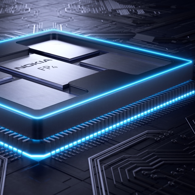 Nokia's FP4 p-chip. The multi-chip module shows five packages: the p-chip die surrounded by four memory stacks. Each stack has five memory die. The p-chip and memory stacks are interconnected using an interposer.
 - Nokia has unveiled the FP4, a 2.4 terabit-per-second network processor that has 6x the throughput of its existing FP3.
- The FP4 is a four-IC chipset implemented using 16nm CMOS FinFET technology. Two of the four devices in the chipset are multi-chip modules.
- The FP4 uses 56 gigabit-per-second serial-deserialiser (serdes) technology from Broadcom, implemented using PAM-4 modulation. It also supports terabit flows.
- Nokia announced IP edge and core router platforms that will use the FP4, the largest configuration being a 0.58 petabit switching capacity router.
Much can happen in an internet minute. In that time, 4.1 million YouTube videos are viewed, compared to 2.8 million views a minute only last year. Meanwhile, new internet uses continue to emerge. Take voice-activated devices, for example. Amazon ships 50 of its Echo devices every minute, almost one a second.
Given all that happens each minute, predicting where the internet will be in a decade’s time is challenging. But that is the task Alcatel-Lucent’s (now Nokia’s) chip designers set themselves in 2011 after the launch of its FP3 network processor chipset that powers its IP-router platforms.
Six years on and its successor - the FP4 - has just been announced. The FP4 is the industry’s first multi-terabit network processor that will be the mainstay of Nokia’s IP router platforms for years to come.
Cloud-scale routing
At the FP4’s launch, Nokia’s CEO, Rajeev Suri, discussed the ‘next chapter’ of the internet that includes smart cities, new higher-definition video formats and the growing number of connected devices.
IP traffic is growing at a compound annual growth rate (CAGR) of 25 percent through to 2022, according to Nokia Bell Labs, while peak data rates are growing at a 39 percent CAGR. Nokia Bell Labs also forecasts that the number of connected devices will grow from 12 billion this year to 100 billion by 2025.
Basil Alwan, Nokia’s president of IP and optical networks, said the internet has entered the era of cloud-scale routeing. When delivering a cloud service, rarely is the request fulfilled by one data centre. Rather, several data centres are involved in fulfilling the tasks. “One transaction to the cloud is multiplied,” said Alwan.
IP traffic is also becoming more dynamic, while the Internet of Things presents a massive security challenge.
Alwan also mentioned how internet content providers have much greater visibility into their traffic whereas the telcos’ view of what flows in their networks is limited. Hence their interest in analytics to understand and manage their networks better.
These are the trends that influenced the design of the FP4.
We put a big emphasis on making sure we had a high degree of telemetry coming out at the chip level
FP4 goals
Telemetry, the sending of measurement data for monitoring purposes, and network security were two key design goals for the FP4.
 Steve Vogelsang“We put a big emphasis on making sure we had a high degree of telemetry coming out at the chip level,” said Steve Vogelsang, CTO for Nokia's IP and optical business.
Tasks include counters, collecting statistics and packet copying. “This is to make sure we have the instrumentation coming off these systems that we can use to drive the [network] analytics platform,” said Vogelsang.
Being able to see the applications flowing in the network benefits security. Distributed Denial-of-Service (DDoS) attacks are handled by diverting traffic to a ‘scrubbing centre’ where sophisticated equipment separates legitimate IP packets from attack traffic that needs scrubbing.
The FP4 supports the deeper inspection of packets. “Once we identify a threat, we can scrub that traffic directly in the network,” said Vogelsang. Nokia claims that that the FP4 can deal with over 90 percent of the traffic that would normally go to a scrubbing centre.
Chipset architecture
Nokia’s current FP3 network processor chipset comprises three devices: the p-chip network processor, the q-chip traffic manager and the t-chip fabric interface device.
The p-chip network processor inspects packets and performs table look-ups using fast-access memory to determine where packets should be forwarded. The q-chip is the traffic manager that oversees the packet flows and decides how packets should be dealt with, especially when congestion occurs. The third FP3 chip is the t-chip that interfaces to the router fabric.
The FP4 retains the three chips and adds a fourth: the e-chip - a media access controller (MAC) that parcels data from the router’s client-side pluggable optical modules for the p-chip. However, while the FP4 retains the same nomenclature for the chips as the FP3, the CMOS process, chip architecture and packaging used to implement the FP4 are significantly more advanced.
The FP4 can deal with over 90 percent of the traffic that would normally go to a scrubbing centre
Nokia is not providing much detail regarding FP4 chipset's architecture, unlike the launch of the FP3. “We wanted to focus on the re-architecture we have gone through,” said Vogelsang. But looking at the FP3 design, insight can be gained as to how the FP4 has likely changed.
The FP3’s p-chip uses 288 programmable cores. Each programmable core can process two instructions each clock cycle and is clocked at 1GHz.
The 288 cores are arranged as a 32-row-by-9-column array. Each row of cores can be viewed as a packet-processing pipeline. A row pipeline can also be segmented to perform independent tasks. The array’s columns are associated with table look-ups. The resulting FP3 p-chip is a 400-gigabit network processor.
Vogelsang said there is limited scope to increase the clock speed of the FP4 p-chip beyond 1GHz. Accordingly, the bulk of the FP4’s sixfold throughput improvement is the result of a combination of programmable core enhancements, possible a larger core array and, most importantly, system improvements. In particular, the memory architecture is now packaged within the p-chip for fast look-ups, while the chipset’s input-output lanes have been boosted from 10 gigabits-per-second (Gbps) to 50Gbps.
Nokia has sought to reuse as much of the existing microcode to program the cores for the FP4 p-chip but has added new instructions to take advantage of changes in the pipeline.
Software compatibility already exists at the router operating system level. The same SROS router operating system runs on Nokia’s network processors, merchant hardware from the like of Broadcom and on x86 instruction-set microprocessors in servers using virtualisation technology.
Such compatibility is achieved using a hardware abstraction layer that sits between the operating system and the underlying hardware. “The majority of the software we write has no idea what the underlying hardware is,” said Vogelsang.
Nokia has a small team of software engineers focussed on the FP4’s microcode changes but, due to the hardware abstraction layer, such changes are transparent to the main software developers.
The FP3’s traffic manager, the q-chip, comprises four reduced instruction set computer (RISC) cores clocked at 900MHz. This too has been scaled up for the FP4 but Nokia has not given details.
The t-chip interfaces to the switch fabric that sits on a separate card. In previous generations of router products, a mid-plane is used, said Nokia. This has been scrapped with the new router products being announced. Instead, the switch cards are held horizontally in the chassis and the line cards are vertical. “A bunch of metal guides are used to guide the two cards and they directly connect to each other,” said Vogelsang. “The t-chips are what interface to these connectors inside the system.”
The MAC e-chip interfaces to the line card’s pluggable modules and support up to a terabit flow. Indeed, the MAC will support integer multiples of 100 Gigabit Ethernet from 100 gigabit to 1 terabit. Nokia has a pre-standard implementation of FlexMAC that allows it to combine lanes across multiple transceivers into a single interface.
Nokia will have line cards that support 24 or 36 QSFP-DD pluggable modules, with each module able to support 400 Gigabit Ethernet.
The FP4 is also twice as power efficient, consuming 4 gigabit/W.
We wanted to make sure we used a high-volume chip-packaging technology that was being driven by other industries and we found that in the gaming industry
Design choices
One significance difference between the two network processor generations is the CMOS process used. Nokia skipped 28nm and 22nm CMOS nodes to go from 40nm CMOS for the FP3 to 16nm FinFET for the FP4. “We looked at that and we did not see all the technologies we would need coming together to get the step-function in performance that we wanted,” said Vogelsang.
Nokia also designed its own memory for the FP4.
“A challenge we face with each generation of network processor is finding memories and memory suppliers that can offer the performance we need,” said Vogelsang. The memory Nokia designed is described as intelligent: instructions can effectively be implemented during memory access and the memory can be allocated to do different types of look-up and buffering, depending on requirements.
Another key area associated with maximising the performance of the memory is the packaging. Nokia has adopted multi-chip module technology for the p-chip and the q-chip.
“We wanted to make sure we used a high-volume chip-packaging technology that was being driven by other industries and we found that in the gaming industry,” said Vogelsang, pointing out that the graphics processing unit (GPU) has similar requirements to those of a network processor. GPUs are highly memory intensive while manipulating bits on a screen is similar to manipulating headers and packets.
The resulting 2.5D packaged p-chip comprises the packet processor die and stacks of memory. Each memory stack comprises 5 memory die. All sit on an interposer substrate - itself a die that is used for dense interconnect of devices. The resulting FP4 p-chip is thus a 22-die multi-chip module.
“Our memory stacks are connected at the die edges and do not use through-silicon vias,” said Vogelsang. “Hence it is technically a 2.5D package [rather than 3D].”
The q-chip is also implemented as a multi-chip module containing RISC processors and buffering memory, whereas the router fabric t-chip and MAC e-chip are single-die ICs.
The FP4’s more advanced CMOS process also enables significantly faster interfaces. The FP4 uses PAM-4 modulation to implement 56Gbps interfaces. “You really need to run those bit rates much much higher to get the traffic into and out of the chip,” said Vogelsang.
Nokia says it is using embedded serialiser-deserialiser interface technology from Broadcom.
Next-gen routers
Nokia has also detailed the IP edge and core routers that will use the FP4 network processor.
The 7750 Service Router (SR-s) edge router family will support up to 144 terabits in a single shelf. This highest capacity configuration is the 7750 SR-14. It is a 24-rack-unit-plus-the-power-supply high chassis and supports a dozen line cards, each 12Tbps when using 100-gigabit modules, or 24x400GbE when using QSFP-DD modules.
Another new platform is the huge 7950 Extensible Routing System (XRS-XC) IP core router which can be scaled to 576 terabits - over half a petabit - when used in a six-chassis configuration. Combining the six chassis does not make require the use of front-panel client-side interfaces. Instead, dedicated interfaces are used with active optical cables to interlink the chassis.
The first router products will be shipped to customers at the year end with general availability expected from the first quarter of 2018.