
Intel targets 5G fronthaul with a 100G CWDM4 module
- Intel announced at ECOC that it is sampling a 10km extended temperature range 100-gigabit CWDM4 optical module for 5G fronthaul.
- Another announced pluggable module pursued by Intel is the 400 Gigabit Ethernet (GbE) parallel fibre DR4 standard.
- Intel, a backer of the CWDM8 MSA, says the 8-wavelength 400-gigabit module will not be in production before 2020.
Intel has expanded its portfolio of silicon photonics-based optical modules to address 5G mobile fronthaul and 400GbE.
 Robert BlumAt the European Conference on Optical Communication (ECOC) being held in Rome this week, Intel announced it is sampling a 100-gigabit CWDM4 module in a QSFP form factor for wireless fronthaul applications.
The CWDM4 module has an extended temperature range, -20°C to +85°C, and a 10km reach.
“The final samples are available now and [the product] will go into production in the first quarter of 2019,” says Robert Blum, director of strategic marketing and business development at Intel’s silicon photonics product division.
Intel also announced it will support the 400GBASE-DR4, the IEEE’s 400 GbE standard that uses four parallel fibres for transmit and four for the receive path, each carrying a 100-gigabit 4-level pulse amplitude modulation (PAM-4) signal.
5G wireless
5G wireless will be used for a variety of applications. Already this year the first 5G fixed and mobile wireless services are expected to be launched. 5G will also support massive Internet of Things (IoT) deployments as well as ultra-low latency applications.
The next-generation wireless standard uses new spectrum that includes millimetre wave spectrum in the 24GHz to 40GHz region. Such higher frequency bands will drive small-cell deployments.
5G’s use of new spectrum, small cells and advanced air interface techniques such as multiple input, multiple output (MIMO) antenna technology is what will enable its greater data speeds and vastly expanded capacity compared to the current LTE cellular standard.
 Source: Intel.
The 5G wireless standard will also drive greater fibre deployment at the network edge. And it is here where mobile fronthaul plays a role, linking the remote radio heads at the antennas with the centralised baseband controllers at the central office (see diagram). Such fronthaul links will use 25-gigabit and 100-gigabit links. “We have multiple customers that are excited about the 100-gigabit CWDM4 for these applications,” says Blum
Intel expects demand for 25-gigabit and 100-gigabit transceivers for mobile fronthaul to begin in 2019.
Intel is now producing over one million PSM4 and CWDM4 modules a year
Client-side modules
Intel entered the optical module market with its silicon photonics technology in 2016 with a 100-gigabit PSM4 module, quickly followed by a 100-gigabit CWDM4 module. Intel is now producing over one million PSM4 and CWDM4 modules a year.
Intel will provide customers with 400-gigabit DR4 samples in the final quarter of 2018 with production starting in the second half of 2019. This is when Intel says large-scale data centre operators will require 400 gigabits.
“The initial demand in hyperscale data centres for 400 gigabits will not be for duplex [fibre] but parallel fibre,” says Blum. “So we expect the DR4 to go to volume first and that is why we are announcing the product at ECOC.”
Intel says the advantages of its silicon photonics approach have already been demonstrated with its 100-gigabit PSM4 module. One is the optical performance resulting from the company’s heterogeneous integration technique combining indium-phosphide lasers with silicon photonics modulators on the one chip. Another advantage is scale using Intel’s 300mm wafer-scale manufacturing.
Intel says demand for the 500m-reach DR4 module to go hand-in-hand with that for the 100-gigabit single- wavelength DR1, given how the DR4 will also be used in breakout mode to interface with four DR1 modules.
“We don’t see the DR1 standard competing or replacing 100-gigabit CWDM4,” says Blum. “The 100-gigabit CWDM4 is now mature and at a very attractive price point.”
Intel is a leading proponent of the CWDM8 MSA, an optical module design based on eight wavelengths, each a 50 gigabit-per-second (Gbps) non-return-to-zero (NRZ) signal. The CWDM8 MSA was created to fast-track 400 gigabit interfaces by avoiding the wait for 100-gigabit PAM-4 silicon.
When the CWDM8 MSA was launched in 2017, the initial schedule was to deploy the module by the end of this year. Intel also demonstrated the module working at the OFC show held in March.
Now, Intel expects production of the CWDM8 in 2020 and, by then, other four-wavelength solutions using 100-gigabit PAM-4 silicon such as the 400G-FR4 MSA will be available.
“We just have to see what the use case will be and what the timing will be for the CWDM8’s deployment,” says Blum.
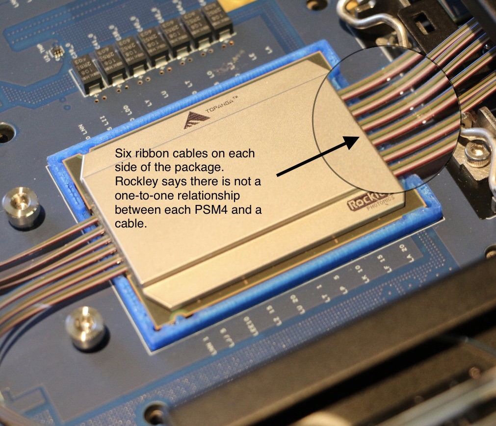
Rockley Photonics showcases its in-packaged design at OFC
The packaged design includes Rockley's own 2 billion transistor layer 3 router chip, and its silicon photonics-based optical transceivers. The layer 3 router chip, described as a terabit device, also includes mixed-signal circuits needed for the optical transceevers' transmit and receive paths.
 Source: Rockley Photonics (annotated by Gazettabyte).
Rockley says it is using 500m-reach PSM4 transceivers for the design and that while a dozen ribbon cables are shown, this does not mean there are 12 100-gigabit PSM4 transceivers. The company is not saying what the total optical input-output is.
 Source: Rockley Photonics (annotated by Gazettabyte).
The company has said it is not looking to enter the marketplace as a switch chip player competing with the likes of Broadcom, Intel, Cavium, Barefoot Networks and Innovium. To develop such a device and remain competitive requires considerable investment and that is not Rockley's focus. Instead, it is using its router chip as a demonstrator to show the marketplace what can be done and that the technology works.
When asked what progress Rockley is making showcasing its technology, its CEO Andrew Rickman said: “It is going very well but nothing we can say publicly."
The switch chip makers continue to use electrical interfaces for their state-of-the-art switches which have a capacity of 12.8 terabits. It still remains to be seen which generation of switch chip will finally adopt in-packaged optics and whether on-board optics designs such as COBO will be adopted first.
For the full interview with CEO Andrew Rickman, click here.
Talking markets: Oclaro on 100 gigabits and beyond
Oclaro’s chief commercial officer, Adam Carter, discusses the 100-gigabit market, optical module trends, silicon photonics, and why this is a good time to be an optical component maker.
Oclaro has started its first quarter 2017 fiscal results as it ended fiscal year 2016 with another record quarter. The company reported revenues of $136 million in the quarter ending in September, 8 percent sequential growth and the company's fifth consecutive quarter of 7 percent or greater revenue growth.
 Adam CarterA large part of Oclaro’s growth was due to strong demand for 100 gigabits across the company’s optical module and component portfolio.
The company has been supplying 100-gigabit client-side optics using the CFP, CFP2 and CFP4 pluggable form factors for a while. “What we saw in June was the first real production ramp of our CFP2-ACO [coherent] module,” says Adam Carter, chief commercial officer at Oclaro. “We have transferred all that manufacturing over to Asia now.”
The CFP2-ACO is being used predominantly for data centre interconnect applications. But Oclaro has also seen first orders from system vendors that are supplying US communications service provider Verizon for its metro buildout.
The company is also seeing strong demand for components from China. “The China market for 100 gigabits has really grown in the last year and we expect it to be pretty stable going forward,” says Carter. LightCounting Market Research in its latest optical market forecast report highlights the importance of China’s 100-gigabit market. China’s massive deployments of FTTx and wireless front haul optics fuelled growth in 2011 to 2015, says LightCounting, but this year it is demand for 100-gigabit dense wavelength-division multiplexing and 100 Gigabit Ethernet optics that is increasing China’s share of the global market.
The China market for 100 gigabits has really grown in the last year and we expect it to be pretty stable going forward
QSFP28 modules
Oclaro is also providing 100-gigabit QSFP28 pluggables for the data centre, in particular, the 100-gigabit PSM4 parallel single-mode module and the 100-gigabit CWDM4 based on wavelength-division multiplexing technology.
2016 was expected to be the year these 100-gigabit optical modules for the data centre would take off. “It has not contributed a huge amount to date but it will start kicking in now,” says Carter. “We always signalled that it would pick up around June.”
One reason why it has taken time for the market for the 100-gigabit QSFP28 modules to take off is the investment needed to ramp manufacturing capacity to meet the demand. “The sheer volume of these modules that will be needed for one of these new big data centres is vast,” says Carter. “Everyone uses similar [manufacturing] equipment and goes to the same suppliers, so bringing in extra capacity has long lead times as well.”
Once a large-scale data centre is fully equipped and powered, it generates instant profit for an Internet content provider. “This is very rapid adoption; the instant monetisation of capital expenditure,” says Carter. “This is a very different scenario from where we were five to ten years ago with the telecom service providers."
Data centre servers and their increasing interface speed to leaf switches are what will drive module rates beyond 100 gigabits, says Carter. Ten Gigabit Ethernet links will be followed by 25 and 50 Gigabit Ethernet. “The lifecycle you have seen at the lower speeds [1 Gigabit and 10 Gigabit] is definitely being shrunk,” says Carter.
Such new speeds will spur 400-gigabit links between the data centre's leaf and spine switches, and between the spine switches. “Two hundred Gigabit Ethernet may be an intermediate step but I’m not sure if that is going to be a big volume or a niche for first movers,” says Carter.
400 gigabit CFP8
Oclaro showed a prototype 400-gigabit module in a CFP8 module at the recent ECOC show in September. The demonstrator is an 8-by-50 gigabit design using 25 gigabaud optics and PAM-4 modulation. The module implements the 400Gbase-LR8 10km standard using eight 1310nm distributed feedback lasers, each with an integrated electro-absorption modulator. The design also uses two 4-wide photo-detector arrays.
“We are using the four lasers we use for the CWDM4 100-gigabit design and we can show we have the other four [wavelength] lasers as well,” says Carter.
Carter says IP core routers will be the main application for the 400Gbase-LR8 module. The company is not yet saying when the 400-gigabit CFP8 module will be generally available.
We can definitely see the CFP2-ACO could support 400 gigabits and above
Coherent
Oclaro is already working with equipment customers to increase the line-side interface density on the front panel of their equipment.
The Optical Internetworking Forum (OIF) has already started work on the CFP8-ACO that will be able to support up to four wavelengths, each supporting up to 400 gigabits. But Carter says Oclaro is working with customers to see how the line-side capacity of the CFP2-ACO can be advanced. “We can definitely see the CFP2-ACO could support 400 gigabits and above,” says Carter. “We are working with customers as to what that looks like and what the schedule will be.”
And there are two other pluggable form factors smaller than the CFP2: the CFP4 and the QSFP28. “Will you get 400 gigabits in a QSFP28? Time will tell, although there is still more work to be done around the technology building blocks,” says Carter.
Vendors are seeking the highest aggregate front panel density, he says: “The higher aggregate bandwidth we are hearing about is 2 terabits but there is a need to potentially going to 3.2 and 4.8 terabits.”
Silicon photonics
Oclaro says it continues to watch closely silicon photonics and to question whether it is a technology that can be brought in-house. But issues remain. “This industry has always used different technologies and everything still needs light to work which means the basic III-V [compound semiconductor] lasers,” says Carter.
“Producing silicon photonics chips versus producing packaged products that meet various industry standards and specifications are still pretty challenging to do in high volume,” says Carter. And integration can be done using either silicon photonics or indium phosphide. “My feeling is that the technologies will co-exist,” says Carter.
Intel's 100-gigabit silicon photonics move
Intel has unveiled two 100-gigabit optical modules for the data centre made using silicon photonics technology.
 Alexis Bjorlin
The PSM4 and CWDM4/CLR4 100-gigabit modules mark the first commercial application of a hybrid integration technique for silicon photonics, dubbed heterogeneous integration, that Intel has been developing for years.
Intel's 100-gigabit module announcement follows the news that Juniper Networks has entered into an agreement to acquire start-up, Aurrion, for $165 million. Aurrion is another silicon photonics player developing this hybrid integration technology for its products.
Hybrid integration
With heterogeneous integration, materials such as indium phosphide and gallium arsenide can be bonded to the silicon substrate before the 300mm wafer is processed to produce the optical circuit. Not only can lasers be added to silicon but other active devices such as modulators and photo-detectors as well as passive functions such as isolators and circulators.
There is no alignment needed; we align the laser with lithography
Intel is using the technique to integrate the laser as part of the 100-gigabit transceiver designs.
"Once we apply the light-emitting material down to the silicon base wafer, we define the laser in silicon," says Alexis Bjorlin, vice president and general manager, Intel Connectivity Group. “There is no alignment needed; we align the laser with lithography.”
Intel claims it gets the highest coupling efficiency between the laser and the optical waveguide and modulator because it is lithographically defined and requires no further alignment.
100-gigabit modules
Intel is already delivering the 100-gigabit PSM4 module. “First volume shipments are happening now,” says Bjorlin. Microsoft is one Internet content provider that is using Intel’s PSM4.
The chip company is also sampling a 100-gigabit CWDM4 module that also meets the more demanding CLR4 Alliance’s optical specification. The 100-gigabit CLR4 module can be used without forward-error correction hardware and is favoured for applications where latency is an issue such as high-performance computing.
Intel is not the first vendor to offer PSM4 modules, nor is it the first to use silicon photonics for such modules. Luxtera and Lumentum are shipping silicon photonics-based PSM4 modules, while STMicroelectronics is already supplying its PSM4 optical engine chip.
We are right on the cusp of the real 100-gigabit connectivity deployments
“Other vendors have been shipping PSM4 modules for years, including large quantities at 40 gigabit,” says Dale Murray, principal analyst at LightCounting Market Research. “Luxtera has the clear lead in silicon photonics-based PSM4 modules but a number of others are shipping them based on conventional optics.”
The PSM4 is implemented using four independent 25-gigabit channels sent over a single-mode ribbon fibre. Four fibres are used for transmission and four fibres for receive.
“The PSM4 configuration is an interesting design that allows one laser to be shared among four separate output fibres,” says Murray. “As Luxtera has shown, it is an effective and efficient way to make use of silicon photonics technology.”
The CWDM4 is also a 4x25-gigabit design but uses wavelength-division multiplexing and hence a single-mode fibre pair. The CWDM4 is a more complex design in that an optical multiplexer and demultiplexer are required and the four lasers operate at different wavelengths.
“While the PSM4 module does not break new ground, Intel’s implementation of WDM via silicon photonics in a CWDM4/CLR4 module could be more interesting in a low-cost QSFP28 module,” says Murray. WDM-based QSFP28 modules are shipping from a number of suppliers that are using conventional optics, he says.
Intel is yet to detail when it will start shipping the CWDM4/CLR4 module.
Market demand
Bjorlin says the PSM4 and the CWDM4/CLR4 will play a role in the data centre. There are applications where being able to break out 100-gigabit into 25-gigabit signals as offered by the PSM4 is useful, while other data centre operators prefer a duplex design due to the efficient use of fibre.
“We are right on the cusp of the real 100-gigabit connectivity deployments,” she says.
As for demand, Bjorlin expects equal demand for the two module types in the early phases: “Longer term, we will probably see more demand for the duplex solution”.
LightCounting says that 100-gigabit PSM4 modules took an early lead in the rollout of 100 Gigabit Ethernet, with VCSEL-based modules not far behind.
“Some are shipping CWDM4/CLR4 and we expect that market to ramp,” says Murray. “Microsoft and Amazon Web Services seem to like PSM4 modules while others want to stick with modules that can use duplex fibre.
 Source: Intel
Data centre switching
“One of the most compelling reasons to drive silicon photonics in the future is that it is an integratable platform,” says Bjorlin.
Switch silicon from the likes of Broadcom support 3.2 terabits of capacity but this will increase to 6.4 terabits by next year and 12.8 terabits using 4-level pulse amplitude modulation (PAM-4) signalling by 2018 (see chart). And by 2020, 25.6-terabit capacity switch chips are expected.
The demand for 100 gigabit is for pluggable modules that fit into the front panels of data center switches. But the market is evolving to 400-gigabit embedded optics that sit on the line card, she says, to enable these emerging higher-capacity switches. Intel is a member of the Consortium of On-Board Optics (COBO) initiative that is being led by Microsoft.
“When you get to 25.6-terabit switches, you start to have a real problem getting the electrical signals in and out of the switch chip,” says Bjorlin. This is where silicon photonics can play a role in the future by co-packaging the optics alongside the switch silicon.
“There will be a need for an integrated solution that affords the best power consumption, the best bandwidth-density that we can get and effectively position silicon photonics for optical I/O [input/output],” says Bjorlin. “Ultimately, that co-packaging is inevitable.”
ST makes its first PSM4 optical engine deliveries
What gives Benetti confidence is the demand he is seeing for 100-gigabit transceivers in the data centre. “From my visibility today, the tipping point is 2016,” says Benetti, group vice president and general manager, digital and mixed processes ASIC division at STMicroelectronics.
 Flavio Benetti
Benetti and colleagues at ST have spent the last four years working to bring to market the silicon photonics technology that the chip company licensed from Luxtera.
The company has developed a 300mm-wafer silicon photonics production line at its fabrication plant in Crolles that is now up and running. ST also has its first silicon photonics product - a mid-reach PSM4 100-gigabit optical engine - and has just started its very first deliveries.
At the OFC show in March, ST said it had already delivered samples to one unnamed 'customer partner', possibly Luxtera, and Benetti showed a slide of the PSM4 chips as part of a Lumentum transceiver.
Another ST achievement Benetti highlights is the development of a complete supply chain for the technology. In addition to wafer production, ST has developed electro-optic wafer testing. This allows devices to be probed electrically and optically to select working designs before the wafer is diced. ST has also developed a process to 3D-bond chips.
“We have focussed on building an industrial environment, with a supply chain that can deliver hundreds of thousands and millions of devices,” says Benetti.
PSM4 and CWDM4
ST’s first product, the components for a 4x25 gigabit PSM4 transceiver, is a two-chip design.
One chip is the silicon photonics optical engine which integrates the PSM4’s four modulators, four detectors and the grating couplers used to interface the chip to the fibres. The second chip, fabricated using ST’s 55nm BiCMOS process, houses the transceiver’s associated electronics such as the drivers, and trans-impedance amplifiers.
The two chips are combined using 3D packaging. “The 3D packaging consists of the two dies, one copper-pillar bonded to the other,” says Benetti. “It is a dramatic simplification of the mounting process of an optical module.”
The company is also developing a 100-gigabit CWDM4 transceiver which unlike the PSM4 uses four 25-gigabit wavelengths on a single fibre.
The CWDM4 product will be developed using two designs. The first is an interim, hybrid solution that uses an external planar lightwave circuit-based multiplexer and demultiplexer, followed by an integrated silicon photonics design. The hybrid design is being developed and is expected in late 2017; the integrated silicon photonics design is due in 2018.
With the hybrid design, it is not just a question of adding a mux-demux to the PSM4 design. “The four channels are each carrying a different wavelength so there are some changes that need to be done to the PSM4,” says Benetti, adding that ST is working with partners that will provide the mux-demux and do the integration.
We need to have a 100-gigabit solution in high volume for the market, and the pricing pressure that is coming has convinced us that silicon photonics is the right thing to do
Opportunities
Despite the growing demand for 100-gigabit transceivers that ST is seeing, Benetti stresses that these are not 'mobile-phone wafer volumes'. “We are much more limited in terms of wafers,” he says. Accordingly, there is probably only room for one or two large fabs for silicon photonics globally, in his opinion.
So why is ST investing in a large production line? For Benetti, this is an obvious development for the company which has been a provider of electrical ICs for the optical module industry for years.
“ST has entered silicon photonics to provide our customers with a roadmap,” says Benetti. “We need to have a 100-gigabit solution in high volume for the market, and the pricing pressure that is coming has convinced us that silicon photonics is the right thing to do.”
It also offers chip players the possibility of increasing its revenues. “The optical engine integrates all the components that were in the old-fashioned modules so we can increase our revenues there,” he says.
ST is tracking developments for 200-gigabit and 400-gigabit links and is assessing whether there is enough of an opportunity to justify pursuing 200-gigabit interconnects.
For now though, it is seeing strong pricing pressure for 100-gigabit links for reaches of several hundred meters. “We do not think we can compete for very short reach distances,” says Benetti. “We will leave that to VCSELs until the technology can no longer follow.” As link speeds increase, the reach of VCSEL links diminishes. “We will see more room for silicon photonics but this is not the case in the short term,” says Benetti.
Market promise
People have been waiting for years for silicon photonics to become a reality, says Benetti. “My target is to demonstrate it [silicon photonics] is possible, that we are serious in delivering parts to the market in an industrial way and in volumes that have not been delivered before.”
To convince the market, it is not just showing the technological advantages of silicon photonics but the fact that there is a great simplification in constructing the optical module along with the ability to deliver devices in volume. “This is the point,” he says.
Benetti’s other role at ST is overseeing advanced networking ASICs. He argues that over the mid- to long-term, there needs to be a convergence between ASIC and optical connectivity.
“Look at a switch board, for example, you have a big ASIC or two in the middle and a bunch of optical modes on the side,” says Benetti. For him, the two technologies - photonics and ICs - are complementary and the industry’s challenge is to make the two live together in an efficient way.
ECOC 2015 Review - Final Part
Part 2 - Client-side component and module developments
- The first SWDM Alliance module shown
- More companies detail CWDM4, CLR4 and PSM4 mid-reach modules
- 400 Gig datacom technologies showcased
- The CFP8 MSA for 400 Gigabit Ethernet unveiled
 The CFP MSA modules including the newest CFP8. Source: Finisar
- Lumentum and Kaiam use silicon photonics for mid-reach modules
- Finisar demonstrates a 10 km 25 Gig SFP28, and low-latency 25 Gig and 100 Gig SR4 interfaces
Shortwave wavelength-division multiplexing
Finisar demonstrated the first 100 gigabit shortwave wavelength-division multiplexing (SWDM) module at ECOC. Dubbed the SWDM4, the 100 gigabit interface supports WDM over multi-mode fibre. Finisar showed a 40 version at OFC earlier this year. “This product [the SWDM4] provides the next step in that upgrade path,” says Rafik Ward, vice president of marketing at Finisar.
The SWDM Alliance was formed in September to exploit the large amount of multi-mode fibre used by enterprises. The goal of the SWDM Alliance is to extend the use of multi-mode fibre by enabling link speeds beyond 10 gigabit.
“We believe if you can do something with multi-mode fibre, you can achieve cost points that are not achievable with single-mode fibre,” says Ward. “SWDM4 allows us to have not only low-cost optics on either end, but allows customers to reuse their installed fibre.”
The SWDM4 interface uses four 25 gigabit VCSELs operating at wavelengths sufficiently apart that cooling is not required. “By having this [wavelength] gap, you can keep to relatively low-cost components like for multiplexing and de-multiplexing,” says Ward.
The 100 Gig SWDM4 achieves 70 meters over OM3 fibre and 100 meters over OM4 fibre. SWDM can scale beyond 100 gigabit, says Ward, but the challenge with multi-mode fibre remains the tradeoff between speed and distance.
Finisar is already shipping SWDM4 alpha samples to customers.
The SWDM Alliance founding members include CommScope, Corning, Dell, Finisar, H3C, Huawei, Juniper Networks, Lumentum, and OFS.
CWDM4, CLR4 and PSM4
Oclaro detailed a 100 gigabit mid-reach QSFP28 module that supports both the CWDM4 multi-source agreement (MSA) and the CLR4 MSA. “We can support either depending on whether, on the host card, there is forward-error correction or not,” says Robert Blum, director of strategic marketing at Oclaro.
Both MSAs have a 2 km reach and use four 25 gigabit channels. However, the CWDM4 uses a more relaxed optical specification as its overall performance is complemented with forward-error correction (FEC) on the host card. The CLR4, in contrast, does not use FEC and therefore requires a more demanding optical specification.
“The requirements are significantly harder to meet for the CLR4 specification,” says Blum. By avoiding FEC, the CLR4 module benefits low-latency applications such as financial trading.
Oclaro showed its dual-MSA module achieving a 10 km reach at ECOC even though the two specifications call for 2 km only. “We have very large margins for the module compared to the specification,” says Blum, adding that customers now need to only qualify one module to meet their CWDM4 or CLR4 line card needs.
Other optical module vendors that announced support for CWDM4 in a QSFP28 module include Source Photonics, whose module is also CLR4-compliant. Kaiam is making CWDM4 and CLR4 modules using silicon photonics as part of its designs.
Lumentum also detailed its CWDM4 and the PSM4, a QSFP28 that uses a single-mode ribbon cable to deliver 100 Gig over 500 meters. Lumentum says its CWDM4 and PSM4 QSFP28 products will be available this quarter. “These 100 gigabit modules are what the hyper-scale data centre operators are clamouring for,” says Brandon Collings, CTO of Lumentum.
The question is who can ramp and support the 100 Gig deployments that are going to happen next year
Lumentum says it is using silicon photonics technology for one of its designs but has not said which. “We have both technologies [indium phosphide and silicon photonics], we use both technologies, and silicon photonics is involved with one of these [modules],” says Collings.
There is demand for both the PSM4 and CWDM4, says Lumentum. Which type a particular data centre operator chooses depends on such factors as what fibre they have or plan to deploy, whether they favour single-mode fibre pairs or ribbon cable, and if their reach requirements are beyond 500 meters.
Quite a few module companies have already sampled [100 Gig] products, says Oclaro’s Blum: “The question is who can ramp and support the 100 Gig deployments that are going to happen next year.”
Technologies for 400 gigabit
Several companies demonstrated technologies that will be needed for 400 gigabit client-side interfaces.
NeoPhotonics and chip company InPhi partnered to demonstrate the use of PAM-4 modulation to achieve 100 gigabit. “To do PAM-4, you need not only the optics but a special PAM-4 DSP,” says Ferris Lipscomb, vice president of marketing at NeoPhotonics.
The 400 Gigabit Ethernet standard under development by the IEEE 802.3bs supports several configurations using PAM-4 including a four-channel parallel single-mode fibre configuration, each at 100 gigabit that will have a 500m reach, and two 8 x 50 gigabit, for 2 km and 10 km links.
The company showcased its 4x28 Gig transmitter optical sub-assembly (TOSA) that uses a photonic integrated circuit comprising electro-absorptive modulated lasers (EMLs). Combined with InPhi’s PAM-4 chip, two channels were combined to achieve 100 gigabit. NeoPhotonics says its EMLs are also capable of supporting 56 gigabaud rates which, coupled with PAM-4, would achieve 100 gigabit single channels.
Lipscomb points out that not only are there several interfaces under development but also various optical form factors. “For 100 Gig and 400 Gig client-side data centre links, there are several competing MSA groups,” says Lipscomb. “The final winning approach has not yet emerged and NeoPhotonics wants its solution to be generic enough so that it supports this winning approach once it emerges.”
Meanwhile, Teraxion announced its silicon photonics-based modulator technology for 100 gigabit (4 x 25 Gig) and 400 gigabit datacom interfaces. “People we talk to are interested in WDM applications for short-reach links,” says Martin Guy, Teraxion’s CTO and strategic marketing.
Teraxion says a challenge using silicon photonics for WDM is supporting a broad band of wavelengths. “People use surface gratings to couple light into the silicon photonics,” says Guy. “But surface gratings have a strong wavelength-dependency over the C-band.”
Teraxion has developed an edge coupler instead which is on the same plane as the propagating light. This compares to a surface grating where light is coupled vertical to the plane.
You hear a lot about the cost of silicon photonics but one of the key advantages is the density you can achieve on the chip itself. Having many modulators in a very small footprint has value for the platform; you can make smaller and smaller transceivers.
“We can couple light efficiently with large-tolerance alignment and our approach can be used for WDM applications,” says Guy. Teraxion’s modulator array can be used for CWDM4 and CLR4 MSAs as well as optical engines for future 400 gigabit datacom systems.
“You hear a lot about the cost of silicon photonics but one of the key advantages is the density you can achieve on the chip itself,” says Guy. “Having many modulators in a very small footprint has value for the platform; you can make smaller and smaller transceivers.”
CFP8 MSA
Finisar demonstrated a 400 gigabit link that included a mock-up of the CFP8 form factor, the latest CFP MSA member being developed to support emerging standards such as 400 Gigabit Ethernet.
The 400 gigabit demonstration implemented the 400GE-SR16 multi-mode standard. A Xilinx FPGA was used to implement an Ethernet MAC and generated 16, 25 Gig channels that were fed to four CFP4 modules, each implementing a 100GBASE-SR4 but collectively acting as the equivalent of the 400GE-SR16. The 16 fibre outputs were then fed to the CFP8 prototype which performed an optical loop-back function, sending the signals back to the CFP4s and FPGA.

The CFP8 will be able to support 6.4 terabit of switching on a 1U card when used in a 2 row by 8 module configuration. The CFP8 has a similar size and power consumption profile of the CFP2. “There is still a lot of work putting an MSA together for 400 gigabit,” says Ward, adding that there is still no timeframe as to when the CFP8 MSA will be completed.
25 Gig SFP28
Finisar also announced at ECOC a 1310nm SFP28 supporting 25 gigabit Ethernet over 10 km, complementing the 850nm SFP28 short reach module it announced at OFC 2015.
Ethernet vendors are designing their next-generation series of switches that use the SFP28, says Finisar, while the IEEE is completing standardising 25 Gigabit Rthernet over copper and multi-mode fibre options.
“There hasn’t yet been a motion to standardise a long-wave interface,” says Ward. “With the demo at ECOC, we have come out with a 25 Gig long-wave interface in advance of a standard.”
Ward points out that the large-scale data centres several years ago only had 40 gigabit as a higher speed option beyond 10 gigabit. Now enterprises will also have a 25 gigabit option.
Ward points out that 25 gigabit compared to 40 Gig delivers an attractive cost-performance. Forty gigabit short-reach and long-reach interfaces are based on four channels at 10 gigabit, whereas 25 gigabit uses one laser and one photo-detector that fit in an SFP28. This compares to a QSFP for 40 Gig.
“25 Gigabit Ethernet is a very interesting interface for the next set of customers after the Web 2.0 players that are looking to migrate beyond 10 gigabit,” said Ward.
Low-latency 25 Gig SR and 100 Gig Ethernet SR4 modules
Also announced by Finisar are 25 Gigabit Ethernet SFP28 SR and 100GE QSFP28 SR4 transceivers that can operate without accompanying FEC on the host board. The transceivers achieve a 30 meter reach on OM3 fibre and 40 meters using OM4 fibre.
“Using FEC simplifies the optical link,” says Ward. “It can take the cost out of the optics by having FEC which gives you additional gain.” But some customers have requested the parts for use without FEC to reduce link latency, similar to those that choose the CLR4 MSA for mid-reach 100 Gig.
Finisar has not redesigned its modules but offering modules that have its higher performing VCSELs and photo-detectors. “Think of it as a simple screen,” says Ward.
Click here for the ECOC 2015 Review - Part 1.
Silicon photonics: "The excitement has gone"
The opinion of industry analysts regarding silicon photonics is mixed at best. More silicon photonics products are shipping but challenges remain.
Part 1: An analyst perspective
"The excitement has gone,” says Vladimir Kozlov, CEO of LightCounting Market Research. “Now it is the long hard work to deliver products.”
 Dale Murray, LightCounting
However, he is less concerned about recent setbacks and slippages for companies such as Intel that are developing silicon photonics products. This is to be expected, he says, as happens with all emerging technologies.
Mark Lutkowitz, principal at consultancy fibeReality, is more circumspect. “As a general rule, the more that reality sets in, the less impressive silicon photonics gets to be,” he says. “The physics is just hard; light is not naturally inclined to work on the silicon the way electronics does.”
LightCounting, which tracks optical component and modules, says silicon photonics product shipments in volume are happening. The market research firm cites Cisco’s CPAK transceivers, and 40 gigabit PSM4 modules shipping in excess of 100,000 units as examples. Six companies now offer 40 gigabit PSM4 products with Luxtera, a silicon photonics player, having a healthy start on the other five.
Indium phosphide and other technologies will not step back and give silicon photonics a free ride
LightCounting also cites Acacia with its silicon photonics-based low-power 100 and 400 gigabit coherent modules. “At OFC, Acacia made a fairly compelling case, but how much of its modules’ optical performance is down to silicon photonics and how much is down to its advanced coherent DSP chip is unclear,” says Dale Murray, principal analyst at LightCounting. Silicon photonics has not shown itself to be the overwhelming solution for metro/ regional and long-haul networks to date but that could change, he says.
Another trend LightCounting notes is how PAM-4 modulation is becoming adopted within standards. PAM-4 modulates two bits of data per symbol and has been adopted for the emerging 400 Gigabit Ethernet standard. Silicon photonics modulators work really well with PAM-4 and getting it into standards benefits the technology, says LightCounting. “All standards were developed around indium phosphide and gallium arsenide technologies until now,” says Kozlov.
You would be hard pressed to find a lot of OEMs or systems integrators that talk about silicon photonics and what impact it is going to have
Silicon photonics has been tainted due to the amount of hype it has received in recent years, says Murray. Especially the claim that optical products made in a CMOS fabrication plant will be significantly cheaper compared to traditional III-V-based optical components.
First, Murray highlights that no CMOS production line can make photonic devices without adaptation. “And how many wafers starts are there for the whole industry? How much does a [CMOS] wafer cost?” he says.
“You would be hard pressed to find a lot of OEMs or systems integrators that talk about silicon photonics and what impact it is going to have,” says Lutkowitz. “To me, that has always said everything.”
![]() Mark Lutkowitz, fibeReality LightCounting highlights heterogeneous integration as one promising avenue for silicon photonics. Heterogeneous integration involves bonding III-V and silicon wafers before processing the two.
Mark Lutkowitz, fibeReality LightCounting highlights heterogeneous integration as one promising avenue for silicon photonics. Heterogeneous integration involves bonding III-V and silicon wafers before processing the two.
This hybrid approach uses the III-V materials for the active components while benefitting from silicon’s larger (300 mm) wafer sizes and advanced manufacturing techniques.
Such an approach avoids the need to attach and align an external discrete laser. “If that can be integrated into a WDM design, then you have got the potential to realise the dream of silicon photonics,” says Murray. “But it’s not quite there yet.”
This poses a real challenge for silicon photonics: it will only achieve low cost if there are sufficient volumes, but without such volumes it will not achieve a cost differential
Murray says over 30 vendors now make modules at 40 gigabit and above: “There are numerous module types and more are being added all the time.” Then there is silicon photonics which has its own product pie split. This poses a real challenge for silicon photonics: it will only achieve low cost if there are sufficient volumes, but without such volumes it will not achieve a cost differential.
“Indium phosphide and other technologies will not step back and give silicon photonics a free ride, and are going to fight it,” says Kozlov. Nor is it just VCSELs that are made in high volumes.
LightCounting expects over 100 million indium phosphide transceivers to ship this year. Many of these transceivers use distributed feedback (DFB) lasers and many are at 10 gigabit and are inexpensive, says Kozlov.
For FTTx and GPON, bi-directional optical subassemblies (BOSAs) now cost $9, he says: “How much lower cost can you get?”
STMicro chooses PSM4 for first silicon photonics product
- Lowers the manufacturing cost of optical modules
- Improves link speeds
- Reduces power consumption
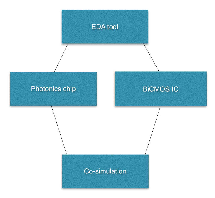 STMicro's in-house silicon photonics EDA. "We will develop the EDA tools to the level needed for the next generation products," says Flavio Benetti.
Module makers rush to fill the 100 Gig mid-reach void
You may give little thought as to how your Facebook page is constructed each time you log in, or the data centre ramifications when you access Gmail. But for the internet giants, what is clear is that they need cheaper, higher-speed optical links to connect their equipment that match the growing size of their hyper-scale data centres.
The challenge for the web players is that existing 100 Gig links are either too short or too expensive. Ten and 40 Gig multimode interfaces span 300m, but at 100 Gig the reach plummets; the existing IEEE 802.3 Ethernet 100GBASE-SR10 and 100GBASE-SR4 multi-mode standards are 100m only. Meanwhile, the 10km reach of the next IEEE interface option, the 100 Gig single-mode 100GBASE-LR4, is overkill and expensive; the LR4 being sevenfold the cost of the 100GBASE-SR10, according to market research firm, LightCounting.
"The largest data centre operators will tell you less than 1km, less than 500m, is their sweet spot," says Martin Hull, director of product management at switch vendor, Arista Networks. Hyperscale data centres use a flatter switching architecture known as leaf and spine. "The flatter switching architectures require larger quantities of economical links between the leaf and spine switches," says Dale Murray, principal analyst at LightCounting.
A 'leaf' can be a top-of-rack switch connecting the servers to the larger-capacity 'spine' of the switch architecture. Operators want 100GbE interfaces with sufficient optical link budget to span 500m and greater distances, to interconnect the leaf and spine, or the spine to the data centre's edge router.
The optical industry has been heeding the web companies' request.
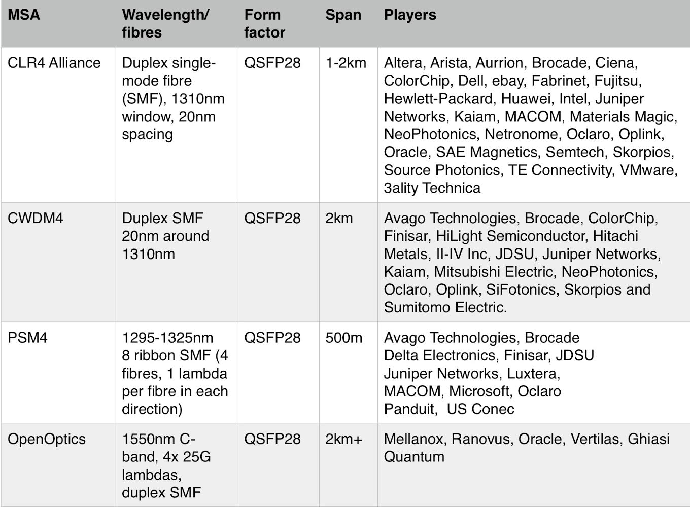
One reason the IEEE 802.3 Ethernet Working Group created the 802.3bm Task Force is to address mid-reach demand by creating a specification for a cheaper 500m interface. Four proposals emerged: parallel single mode (PSM4), coarse WDM (CWDM), pulse amplitude modulation, and discrete multi-tone. But none of the proposals passed the 75% voting threshold to become a standard.
The optical industry has since pursued a multi-source agreement (MSA) strategy to bring the much-needed solutions to market. In the last year, no fewer than four single-mode interfaces have emerged: the CLR4 Alliance, and the CWDM4, PSM4 and OpenOptics MSAs.
"The MSA-based solutions will have two important advantages," says Murray. "All will be much less expensive than a 10km 100Gig LR4 module and all can be accommodated by a QSFP28 form factor."
The 100 GbE PSM4, backed by the leading optical module makers (see table above), differs from the other three designs in using parallel ribbon fibre and having a 500m rather than a 2km reach. The PSM4 uses four 25 Gig channels, each sent over a fibre, such that four fibres are used in each direction. The PSM4 is technically straightforward and is likely to be the most economical for links up to 500m. In contrast, the CLR4, CWDM4 and OpenOptical all use 4x25 Gig WDM over duplex fibre. Thus, while the PSM4 will likely be the cheapest of the four modules, the link's cost advantage is eroded with distance due to the ribbon fibre cost.
The PSM4 is also attractive for secondary applications; the 25 Gig channels could be used as individual 'breakout' links. Already there is industry interest in 25GbE, while the module could be used in future for 32 Gig Fibre Channel and high-density 128 Gig Fibre Channel.
The OpenOptics MSA, backed by Mellanox and start-up Ranovus, operates in the 1550nm C-band and uses dense WDM, whereas the CLR4 Alliance and CWDM4 operate around 1310nm and use CWDM. The 100 GbE OpenOptics is also 4x25 Gig, such that the wavelengths can be spaced far apart but DWDM promises a roadmap for even higher speed interfaces.
The CLR4 Alliance is an Intel-Arista initiative that has garnered wide industry backing, but it is not an MSA. The specification is very similar to the CWDM4. Both the CLR4 and the CWDM4 include forward error correction (FEC) but whereas FEC is fundamental to the CWDM4, it is an option with the CLR4.
"We have focussed on the FEC-enabled [CWDM4] version so that optical manufacturers can develop the lowest possible cost components to support the interface," says Mitchell Fields, senior director, product marketing and strategy, fiber-optics product division at Avago. FEC adds flexibility, he says, not just in relaxing the components' specification but also simplifying module testing.
The backers of CWDM4 and CLR4 are working to align their specifications and while it is likely the two will interoperate, it remains unclear whether the two will merge.
The CWDM4 specification is likely to be completed in September with first products appearing as early as one or two quarters later. Arista points out that it already has a switch that could use CWDM4/ CLR4 modules now if they were available.
John D'Ambrosia, chairman of the Ethernet Alliance, regrets that four specifications have emerged. "My own personal belief is that it would be better for the industry overall if we didn't have so many choices," he says. "But the reality is there are a lot of different applications out there."
LightCounting expects the PSM4 and a merged CWDM offering will find strong market traction. "Avago, Finisar, JDSU and Oclaro are participating in both categories, demonstrating that each has its own value proposition," says Murray.
This article first appeared in the Optical Connections ECOC '14 magazine issue.
For a more detailed article on mid-reach optics, see p28 of the Autumn issue of Fibre Systems, click here
Article Revision: 30/10/2014: Updated members list of the OpenOptics MSA
OFC 2014 product round-up - Final part

The industry is moving at a clip to fill the void in 100 Gig IEEE standards for 100m to 2km links. Until now, the IEEE 10km 100GBASE-LR4 and the 10x10 MSA have been the interfaces used to address such spans.
But responding to data centre operators, optical players are busy developing less costly, mid-reach MSAs, as was evident at the OFC exhibition and conference, held in San Francisco in March.
Meanwhile, existing IEEE 100 Gigabit standards are skipping to the most compact CFP4 and QSFP28 form factors. The -LR4 standard was first announced in a CFP in 2010, and moved to the CFP2, half the size of the CFP, in 2013. Now, several companies have detailed CFP4 -LR4 products, while Source Photonics has gone one better, announcing the standard in a QSFP28.
The CFP4 is half the size of the CFP2, while the QSFP28 is marginally smaller than the CFP4 but has a lower power consumption: 3.5W compared to the CFP4's 6W.
 Timeline of some pluggable announcements at recent OFCs. Source: Gazettabyte
The mid-reach landscape
Several interfaces for mid-reach interconnect were detailed at OFC. And since the show, two MSAs have been detailed: the CWDM4 and the CLR4 Alliance.
At OFC, the OpenOptics MSA backed by Mellanox Technologies and Ranovus, was announced. Skorpios Technologies demoed its CLR4 module that has since become the CLR4 Alliance. And vendors discussed the Parallel Single Mode (PSM4) initiative that was first detailed in January.
Switch vendor Mellanox Technologies and module start-up Ranovus announced the OpenOptics MSA at OFC. The QSFP-based MSA uses a single-mode fibre and WDM transmission around 1550nm to address data centre links up to 2km.
Saeid Aramideh of Ranovus says that the MSA using its laser and silicon photonics technologies will deliver significant cost, power and size advantages {add link}. "But the 1550nm WDM connection is open to any technology," says Aramideh, chief marketing and sales officer at Ranovus. "It does not have to be silicon photonics."
The first MSA product, a 100 Gig QSFP28, uses 4x25 Gig channels. "The channel spacing for the MSA is flexible to be 50GHz or more," says Aramideh. The MSA is scalable to 400 Gig and greater rates. The 100 Gig QSFP28 technology is several months away from sampling.
Skorpios Technologies demonstrated its QSFP28-CLR4 transceiver although the details of the MSA have yet to be detailed. Skorpios is a silicon photonics player and uses heterogenous integration where the lasers, modulators, detectors and optical multiplexer and de-multiplexer are monolithically integrated on one chip.
The PSM4 MSA is another initiative designed to tackle the gap between IEEE short and long reach standards. Backed by players such as Avago Technologies, Brocade, JDSU, Luxtera, Oclaro, and Panduit, the 100 Gig standard is defined to operate in the 1295-1325nm spectral window and will have a reach of at least 500m.
ColorChip demonstrated a 100 Gig (4x25 Gig) QSFP28 with a 2km reach at the show. The design uses uncooled directly modulated lasers to achieve the 3.5W power consumption. Since the show Colorchip is one of the member companies backing the CLR4 Alliance and the demoed QSFP matches the first details of the new MSA's spec.
100GBASE-LR4 moves to CFP4 and QSFP28
The IEEE 100GBASE-LR4 standard is transitioning to the smallest modules. At OFC, vendors detailed the first CFP4s while Source Photonics announced the -LR4 in a QSFP28.
Source Photonics says its transceiver consumes 3.5W. The QSFP28 form factor achieves up to a fourfold increase in face plate density compared to the CFP2: up to 48 modules compared to a dozen CFP2 modules, says the company, which expects first QSFP28 -LR4 samples in mid-2014.
Meanwhile, Avago Technologies, Finisar, Fujitsu Optical Components and JDSU all detailed their first CFP4 -LR4 modules.
JDSU says that when it developed the optics for its CFP2 -LR4, it was already eyeing the transition to the CFP4 and QSFP28 form factors. To achieve the -LR4 spec in the 6W CFP4, a key focus are the clock data recover (CDR), driver and trans-impedance amplifier chips. "A decent amount of the power consumption is wrapped up in the ICs that do the CDR and a variety of the digital functions behind the photonics," says Brandon Collings, JDSU's CTO for communications and commercial optical products. JDSU expects general availability of its CFP4 -LR4 later this year.
Finisar's -LR4 is its second CFP4 product; at ECOC 2013 it showcased a 100m, 100GBASE-SR4 CFP4. Finisar says its -LR4 uses distributed feedback (DFB) lasers and consumes 4.5W, well within the CFP4's 6W power profile. At OFC, the CFP4 was demonstrated working with CFP2 and CFP -LR4 modules. Finisar's CFP4 will sample later this year.
Avago announced availability of its -LR4 transmit optical subassembly (TOSA) and receive optical subassembly (ROSA) products for the CFP4, along with its CFP4 module which it says will be available next year. Fujitsu Optical Components also used OFC to demo its CFP4 -LR4.
40km Extended Reach Lite
Oclaro and Finisar detailed a tweak to the 100 Gig Extended Reach standard: the 40km, 100GBASE-ER4.
The IEEE standard uses a power-hungry semiconductor optical amplifier (SOA) prior to the PIN photodetector to achieve 40km. The module vendors have proposed replacing the SOA and PIN with an avalanche photo diode (APD) and external forward error correction to reduce the power consumption while maintaining the optical link budget. The changed spec is dubbed 100GBASE-ER4 Lite.
"Trying to achieve the power envelopes required for the CFP4 and QSFP28 using SOAs is going to be too hard," says Kevin Granucci, vice president of strategy and marketing at Oclaro.
Oclaro demonstrated a ER4-Lite in a CFP2. The module supports 100 Gigabit Ethernet and the Optical Transport Network (OTN) OTU-4 rates, and consumes less than 9W. "We are using the CFP2 as the first proof-of-concept," says Granucci. "For the 6W CFP4 and the 3.5W QSFP28, we think this is the only solution available."
At OFC Finisar demonstrated the link's feasibility, which it refers to as ER4f, using four 28 Gig lasers and four 28 Gig APDs.
Oclaro says it is seeing customer interest in the ER4 Lite, and points out that there are many 10 Gig 40km links deployed, especially in China. "The ER4 Lite will provide an update path to 100 Gig," says Granucci.
VCSELs: serial 40 Gig and the 400 Gig CDFP
Finisar showcased a VCSEL operating at 40 Gig at OFC. State-of-the-art VCSEL interfaces run up to 28 Gig. Finisar's VCSEL demonstration was to show the commercial viability of higher-speed VCSELs for single channel or parallel-array applications. "We believe that VCSELs have not run out of steam," says Rafik Ward, vice president of marketing at Finisar. The 40 Gig VCSEL demonstration used non-return-to-zero (NRZ) signalling, "no higher-order modulation is being used", says Ward.
IBM T.J.Watson Research Center has published an IEEE paper with Finisar involving a 56Gbps optical link based on an 850nm VCSEL.
Finisar also demonstrated an CDFP-based active optical cable. The CDFP is a 400 Gig MSA that uses 16 x 25 Gig VCSEL channels in each direction. Such an interface will address routing, high-performance computing and proprietary interface requirements, says Finisar. The demonstration showcased the technology; Finisar has yet to announce interface products or reaches.
Short reach 100G and 4x16 Gig Fibre QSFPs
Avago Technologies announced a 100GBASE-SR4 implemented using the QSFP28. Avago's I Hsing Tan, segment marketing manager for Ethernet and storage optical transceivers, says there has been a significant ramp in data centre demand for the 40GBASE-SR4 QSFP+ in the last year. "Moving to the next generation, the data centre operator would like to keep the same [switch] density as the QSFP+, and the QSFP28 MSA offers the same form factor," he says.
The QSFP28 differs from the QSFP+ is that its electrical connector is upgraded to handle 28 Gigabit-per-lane data rates. Avago says the -SR4 module will be generally available next year.
Avago also announced a 4x16 Gigabit Fibre Channel QSFP+ transceiver. The industry is transitioning from 8 to 16 Gig Fibre Channel, says Avago, and this will be followed by 32 Gig serial and 4x32 Gig Fibre Channel modules.
The company has announced a 4x16 Gig QSFP+ to continue the increase in platform channel density while the industry transitions from 16 to 32 Gig Fibre Channel. "This solution is going to provide the switch vendor a 3x increase in density at half the power dissipation per channel for 16 Gig Fibre Channel, before the 32 bit Fibre Channel come to maturity in three to five years," says Tan.
Avago has just announced that it has shipped over half a million QSFP+ modules.
Optical engines
TE Connectivity announced its 25 Gig-per-channel optical engine technology. The Coolbit optical engine will be included in four TE Connectivity products planned for this year: 100 Gig QSFP28 active optical cables (AOCs), 100 Gig QSFP28 transceivers, 300 Gig mid-board optical modules, and 400 Gig CDFP AOCs.
Meanwhile, Avago's MiniPod and MicroPod optical engine products now have a reach of 550m when coupled with Corning's ClearCurve OM4 fibre.
"This allows customers in the data centre to go a little bit further and not have to go to single-mode fibre," says Sharon Hall, product line manager for embedded optics at Avago.
For Part 1, click here
Further reading:-
TE Connectivity White Paper: End-to-end Communications with Fiber Optic Technologies, click here
LightCounting: Reflections on OFC 2014: The industry is approaching a critical junction, click here
Ovum at OFC 2014, click here
LightWave OFC 2014 Podcast, click here
Ethernet Alliance Blog: OFC 2014 show and best in class, click here