Inphi unveils first 800-gigabit PAM-4 signal processing chip
Inphi has detailed what it claims is the industry’s first digital signal processor (DSP) chip family for 800-gigabit client-side pluggable modules.
Dubbed Spica, the 4-level pulse-amplitude modulation (PAM-4) DSP family is sampling and is in the hands of customers.
The physical-layer company has also announced its third-generation Porrima family of PAM-4 DSPs for 400-gigabit pluggables.
The Porrima DSP with integrated laser driver has being made using a 7nm CMOS process; until now a 16nm CMOS has been used. Fabricating the chip using the more advanced process will reduce the power consumption of 400-gigabit module designs.
Applications
Eight-hundred-gigabit multi-source agreements (MSAs) will enable a new generation of high-speed optical transceivers to come to market.
The 800G Pluggable MSA developing optical specifications for 800-gigabit pluggable modules, is one that Inphi is promoting, while the QSFP-DD800 MSA is extending the double density form factor for 800 gigabits.

The main two markets driving a need for 800-gigabit modules are artificial intelligence (AI) and data centre switching, says Eric Hayes, senior vice president, networking interconnect at Inphi.
“AI, while still in its infancy, has all these applications and workloads that it can drive,” he says. “But one thing they have in common when we look at the data centres building large AI clusters is that they have very large data sets and lots of data flow.”
The speed of the input-output (I/O) of the AI processors used in the clusters is rising to cope with the data flows.
The second application that requires 800-gigabit modules is the advent of 25.6-terabit Ethernet switches used to network equipment within the data centre.
Inphi says there are two types of 25.6-terabit switch chips emerging: one uses 50-gigabit PAM-4 while the second uses 100-gigabit PAM-4 electrical interfaces.
“The 25.6-terabyte switch with 100-gigabit I/O is wanted for one-rack-unit (1RU) platforms,” says Hayes. “To do that, you need an 800-gigabit module.” Such switches have yet to reach the marketplace.
The first-generation AI processors used 25-gigabit non-return-to-zero (NRZ) signalling for the I/O while many of the devices shipping today use 50-gigabit PAM-4. “The latest designs that are coming to market have 100-gigabit I/O and we have the first DSP offering 100-gigabit on the host side,” says Hayes.
Spica and Porrima ICs
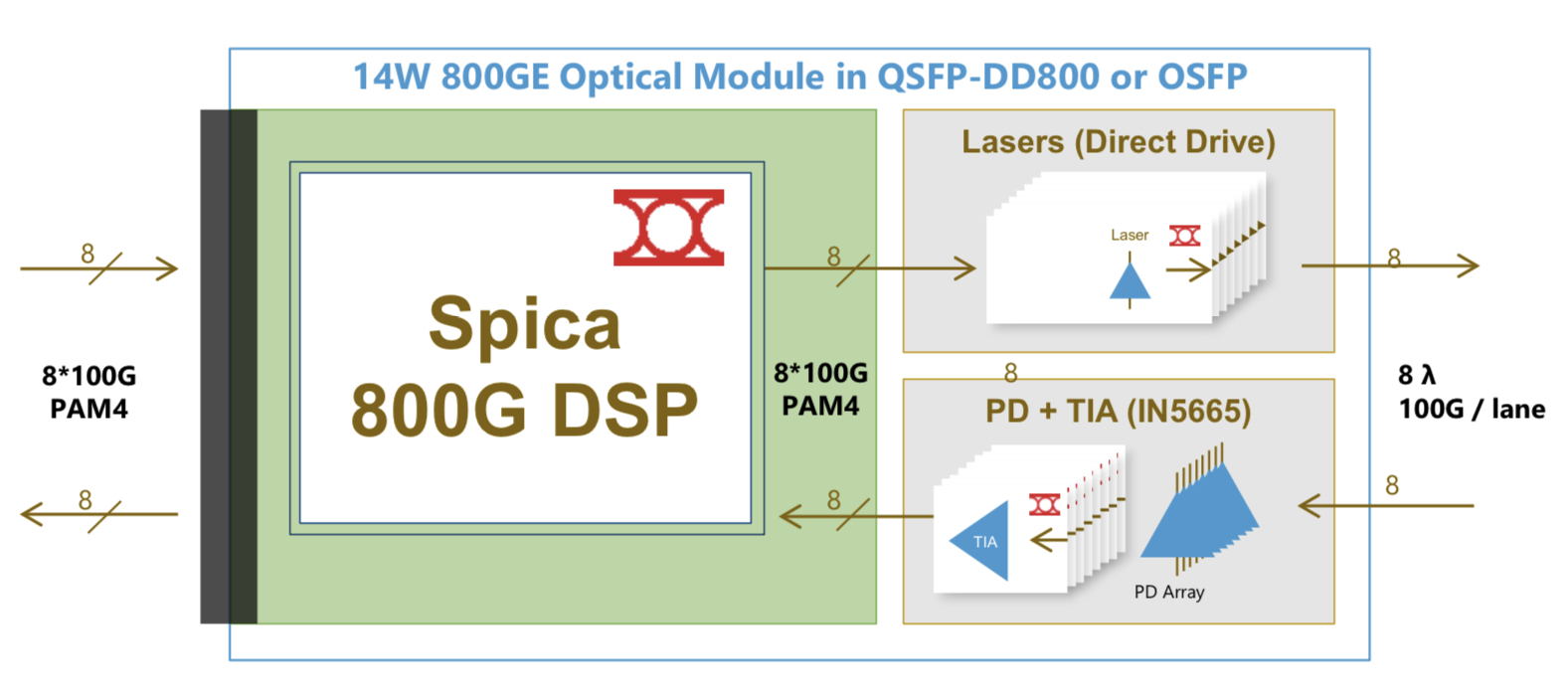
The Spica DSP takes 100-gigabits PAM-4 electrical signals from the host and performs retiming and pre-emphasis to generate the 100-gigabit PAM-4 signals used for modulation the optics before transmission. The laser driver is integrated on-chip.
The transmit path is a simpler design than the Porrima in that the signalling rate is the same at the input and the output. Accordingly, no gearbox circuitry is needed.
The main signal processing is performed at the receiver to recover the sent PAM-4 signals. A hybrid design is used combining analogue and digital signal processing, similar to the design used for the Porrima.
The Spica device supports 2×400-gigabit or 8×100-gigabit module designs and enables 800-gigabit or 8×100-gigabit optical interconnects. The 800-gigabit form factors used are the QSFP-DD800 and the OSFP. Inphi says both designs consume under 14W.
“The first module being built [using the Spica] is the OSFP because the end-user is demanding that, but we also have customers building QSFP-DDs,” says Hayes.
Meanwhile, Inphi’s Porrima family of devices is targeted at the 400G DR4 and 400G FR4 specifications as well as 100-gigabit module designs that use 100-gigabit PAM-4.
The two module types can even be combined when a 400-gigabit pluggable such as a QSFP-DD or an OSFP is used in breakout mode to feed four 100-gigabit modules implement using such form factors as the QSFP, uQSFP or SFP-DD.
Transitioning the Porrima to a 7nm process saves 1.5W of power, says Hayes, resulting in an 8W 400-gigabit module. The latest Porrima is sampling and is with customers.
Roadmap
Inphi says optical modules using the Spica DSP will be deployed in volume from the second half of 2021.
Before then, the DSP will be tested as part of customers’ module designs, then be integrated with the software before the complete 800-gigabit module is tested.
“There will then be interoperability testing between the modules once they become available and then small pilot networks using 800-gigabit modules will be built and tested before the go-ahead to mass deployment,” says Hayes.
All these stages will require at least a year’s work.

Inphi adds a laser driver to its 100-gigabit PAM-4 DSP
Inphi has detailed its second-generation Porrima chip family for 100-gigabit single-wavelength optical module designs.

Source: Inphi
The Porrima family of devices is targeted at the 400G DR4 and 400G FR4 specifications as well as 100-gigabit module designs that use 100-gigabit 4-level pulse-amplitude modulation (PAM-4). Indeed, the two module types can be combined when a 400-gigabit pluggable such as a QSFP-DD or an OSFP is used in breakout mode to feed four 100-gigabit modules using such form factors as the QSFP, uQSFP or SFP-DD.
The Gen2 family has been launched a year after the company first announced the Porrima. The original 400-gigabit and 100-gigabit Porrima designs each have three ICs: a PAM-4 digital signal processor (DSP), a trans-impedance amplifier (TIA) and a laser-driver.
“With Gen2, the DSP and laser driver are integrated into a single monolithic CMOS chip, and there is a separate amplifier chip,” says Siddharth Sheth, senior vice president, networking interconnect at Inphi. The benefit of integrating the laser driver with the DSP is lower cost, says Sheth, as well as a power consumption saving.
The second-generation Porrima family is now sampling with general availability expected in mid-2019.
PAM-4 families
Inphi has three families of PAM-4 ICs targeting 400-gigabit interfaces: the Polaris, Vega and Porrima.
The Polaris, Inphi’s first product family, uses a 200-gigabit die and two are used within the same package for 400-gigabit module designs. As well as the PAM-4 DSP, the Polaris family also comprises two companion chips: a laser driver and an amplifier.
Inphi’s second family is the Vega, a 8x50-gigabit PAM-4 400-gigabit DSP chip that sits on a platform’s line card.
“The chip is used to drive backplanes and copper cables and can be used as a retimer chip,” says Sheth.

Siddharth Sheth
“For the Porrima family, you have a variant that does 4x100-gigabit and a variant that does 1x100-gigabit,” says Sheth. The Porrima can interface to a switch chip that uses either 4x25-gigabit non-return-to-zero (NRZ) or 2x50-gigabit PAM-4 electrical signals.
Why come out with a Gen2 design only a year after the first Porrima? Sheth says there was already demand for 400-gigabit PAM-4 chips when the Porrima first became available in March 2018. Optical module makers needed such chips to come to market with 400-gigabit modules to meet the demand of an early hyperscale data centre operator.
“Now, the Gen2 solution is for the second wave of customers,” says Sheth. “There are going to be two or three hyperscalers coming online in 2020 but maybe not as aggressively as the first hyperscaler.” These hyperscalers will be assessing the next generation of 400-gigabit PAM-4 silicon available, he says.
The latest design, like the first generation Porrima, is implemented using 16nm CMOS. The DSP itself has not been modified; what has been added is the laser-driver circuitry. Accordingly, it is the transmitter side that has been changed, not the receiver path where Inphi does the bulk of the signal processing. “We did not want to change a whole lot because that would require a change to the software,” he says.
A 400-gigabit optical module design using the first generation Porrima consumes under 10W but only 9W using the Gen2. The power saving is due to the CMOS-based laser driver consuming 400mW only compared to a gallium arsenide or silicon germanium-based driver IC that consumes between 1.6W to 2W, says Inphi.
The internal driver can achieve transmission distances of 500m while a standalone driver will still be needed for longer 2km spans.
Sheth says that the advent of mature low-swing-voltage lasers will mean that the DSP’s internal driver will also support 2km links.
PAM-4 DSP
The aim of the DSP chip is to recover the transmitted PAM-4 signal. Sheth says PAM-4 chip companies differ in how much signal processing they undertake at the transmitter and how much is performed at the receiver.
“It comes down to a tradeoff, we believe that we are better off putting the heavier signal processing on the receive side,” says Sheth.
Inphi performs some signal processing on the transit side where transmit equalisation circuits are used in the digital domain, prior to the digital-to-analogue converter.
The goal of the transmitter is to emit a signal with the right amplitude, pre-emphasis, and having a symmetrical rise and fall. But even generating such a signal, the PAM-4 signal recovered at the receiver may look nothing like the signal sent due to degradations introduced by the channel. “So we have to do all kind of tricks,” he says.
Inphi uses a hybrid approach at the receiver where some of the signal processing is performed in the analogue domain and the rest digitally. A variable-gain amplifier is used up front to make sure the received signal is at the right amplitude and then feed-forward equalisation is performed. After the analogue-to-digital stage, post equalisation is performed digitally.
Sheth says that depending on the state of the received signal - the distortion, jitter and loss characteristics it has - different functions of the DSP may be employed.
One such DSP function is a reflection canceller that is turned on, depending on how much signal reflection and crosstalk occur. Another functional block that can be employed is a maximum likelihood sequence estimator (MLSE) used to recover a signal sent over longer distances. In addition, forward-error correction blocks can also be used to achieve longer spans.
“We have all sorts of knobs built into the chip to get an error-free link with really good performance,” says Sheth. “At the end of the day, it is about closing the optical link with plenty of margin.”
What next?
Sheth says the next-generation PAM-4 design will likely use an improved DSP implemented using a more advanced CMOS process.
“We will take the learning from Gen1 and Gen2 and roll it into a ‘Gen3’,” says Sheth.
Such a design will also be implemented using a 7nm CMOS process. “We are now done with 16nm CMOS,” concludes Sheth.