
NeoPhotonics showcases a CFP2-ACO roadmap to 400G
The company demonstrated the CFP2-ACO module transmitting at 100 gigabit using polarisation multiplexed, quadrature phase-shift keying (PM-QPSK) modulation at the recent OFC show. The line-side module is capable of transmitting over 1,000km and also supports PM-16QAM that doubles capacity over metro network distances.
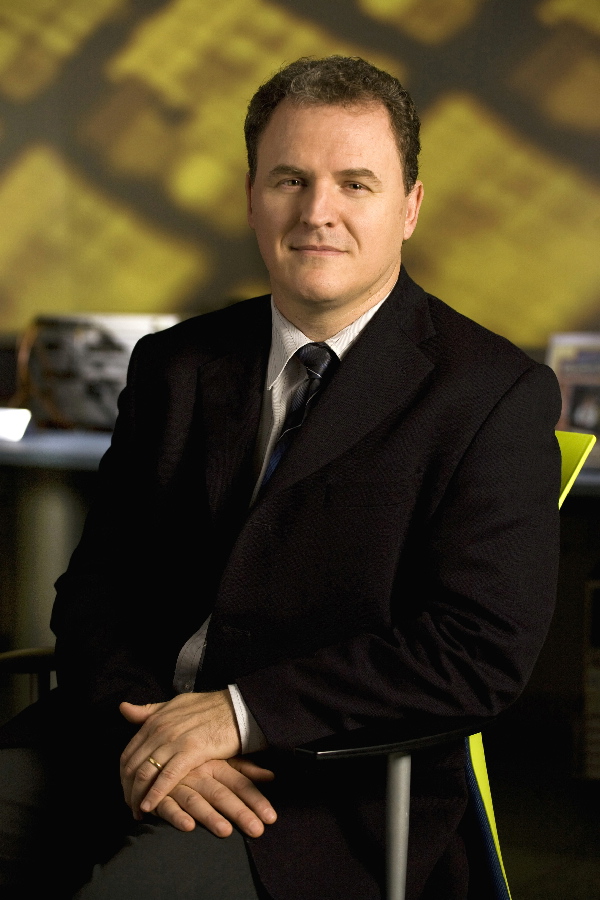
 Ferris LipscombThe CFP2-ACO is a Class 3 design: the control electronics for the modulator and laser reside on the board, alongside the coherent DSP-ASIC chip.
At OFC, NeoPhotonics also demonstrated single-wavelength 400-gigabit transmission using more advanced modulation and a higher symbol rate, and a short-reach 100-gigabit link for inside the data centre using 4-level pulse-amplitude modulation (PAM4) signalling.
Roadmap to 400 gigabit
One benefit of the CFP2-ACO is that the pluggable module can be deployed only when needed. Another is that the optics will work with coherent DSP-ASICs for different systems vendors and merchant chip suppliers.
“After a lot of technology-bragging about the CFP2-ACO, this is the year it is commercial,” says Ferris Lipscomb, vice president of marketing at NeoPhotonics.
Also demonstrated were the components needed for a next-generation CFP2-ACO: NeoPhotonics’ narrow line-width tunable laser and its higher-bandwidth integrated coherent receiver. To achieve 400 gigabit, 32-QAM and a 45 gigabaud symbol rate were used.
Traditional 100-gigabit coherent uses a 32-gigabaud symbol rate. That combined with QPSK and the two polarisations results in a total bit rate of 2 polarisations x 2bits/symbol x 32 gigabaud or 128 gigabits: a 100-gigabit payload and the rest overhead bits. Using 32-QAM instead of QPSK increases the number of bits encoded per symbol from 2 to 5, while increasing the baud rate from 32 to 45 gigabaud adds a speed-up factor of 1.4. Combining the two, the resulting bit rate is 45 gigabaud x 5bits/symbol x 2 polarisations or 450 gigabit overall.
After a lot of technology-bragging about the CFP2-ACO, this is the year it is commercial
Using 32-QAM curtails the transmission distance to 100km due to the denser constellation but such distances are suited for data centre interconnect applications.
“That was the demo [at OFC] but the product is also suitable for metro distances of 500km using 16-QAM and long-haul of 1,000km using 200 gigabit and 8-QAM,” says Lipscomb.
PAM4
The PAM4 demonstration highlighted NeoPhotonics’ laser and receiver technology. The company showcased a single-wavelength link running at 112 gigabits-per-second using its 56Gbaud externally modulated laser (EML) with an integrated driver. The PAM4 link can span 2km in a data centre.
“What is not quite ready for building into modules is the [56Gbaud to 112 gigabit PAM4] DSP, which is expected to be out in the middle to the second half of the year,” says Lipscomb. The company will develop its own PAM4-based optical modules while selling its laser to other module makers.
Lipscomb says four lanes at 56 gigabaud using PAM4 will deliver a cheaper 400-gigabit solution than eight lanes, each at 25 gigabaud.
Silicon Photonics
NeoPhotonics revealed that it is supplying new 1310nm and 1550nm distributed feedback (DFB) lasers to optical module players that are using silicon photonics for their 100-gigabit mid-reach transceivers. These include the 500m PSM-4, and the 2km CWDM4 and CLR4.
Lipscomb says the benefits of its lasers for silicon photonics include their relatively high output power - 40 to 60mW - and the fact that the company also makes laser arrays which are useful for certain silicon photonics applications.
NeoPhotonics’ laser products have been for 100-gigabit modules with reaches of 2km to 10km. “Silicon photonics is usually used for shorter reaches of a few hundred meters,” says Lipscomb. “This new product is our first one aimed at the short reach data centre market segment.”
“Our main products have been for 100-gigabit modules for the longer reaches of 2km to 10km,” says Lipscomb. “Silicon photonics is usually used for shorter reaches of a few hundred meters, and this new [laser] product is our first one aimed at the short reach data centre market segment."
The company says it has multiple customer engagements spanning various wavelength plans and approaches for Nx100-gigabit data centre transceiver designs. Mellanox Technologies is one vendor using silicon photonics that NeoPhotonics is supplying.
BT makes plans for continued traffic growth in its core
Part 1
 Kevin Smith: “A lot of the work we are doing with the trials have demonstrated we can scale our networks gracefully rather than there being a brick wall of a problem.”
BT is confident that its core network will accommodate the expected IP traffic growth for the next decade. Traffic in BT’s core is growing at between 35 and 40 percent annually, compared to the global average growth rate of 20 to 30 percent. BT attributes the higher growth to the rollout of fibre-based broadband across the UK.
The telco is deploying 100-gigabit wavelengths in high-traffic areas of its network. “These are key sites where we're running out of wavelengths such that we need to implement higher-speed ones,” says Kevin Smith, research leader for BT’s transport networks. The operator is now trialling 200-gigabit wavelengths using polarisation multiplexing, 16-quadrature amplitude modulation (PM-16QAM).
Adopting higher-order modulation increases capacity and spectral efficiency but at the expense of a loss in system performance which can be significant.
Systems vendors use polarisation-multiplexed, quadrature phase-shift keying (PM-QPSK) for 100-gigabit wavelengths. Moving to PM-16QAM doubles the bits on the wavelength but the received data has less tolerance to noise. The result is a 6-decibel loss compared to PM-QPSK, such that the transmission distance drops to a quarter. If PM-QPSK spans a 4,000km link, using PM-16QAM the reach on the same link is only 1,000km.
The transmitted capacity can also be increased by using pulse-shaping at the transmitter to cram a wavelength into a narrower channel. BT’s existing optical network uses fixed 50GHz-wide channels. But in a recent network trial with Huawei, a 3 terabit super-channel was transmitted over a 360km link using a flexible grid.
The super-channel comprised 15 channels, each carrying 200 gigabit using PM-16QAM. Using the flexible grid, each carrier occupied a 33.5GHz channel, increasing fibre capacity by a factor of 1.5 compared to a 50GHz fixed-grid. “For 16-QAM, it [33.5GHz] is pretty close to the limit,” says Smith.
Increasing the baud rate is the most structurally-efficient way to accommodate the high speed
Another way to boost the carrier’s data as well as reduce system cost is to up the signalling rate. Current optical transport systems use a 30Gbaud symbol rate. Here, two carriers each using PM-16QAM are needed to deliver 400 gigabit. Doubling the symbol rate to 60Gbaud enables a single 400 gigabit wavelength. Doubling the baud rate also halves a platform’s transponder count, reducing the overall cost-per-bit, and increases platform density.
“Increasing the baud rate is the most structurally-efficient way to accommodate the high speed,” says Smith. Going to 16QAM increases the data that is carried but at the expense of reach. By increasing the baud rate, reach can be extended while also keeping the modulation rate at a lower level, he says.
BT says it is seeing signs of such ‘flexrate’ transponders that can adapt modulation format and baud rate. “This is a very interesting area we can mine,” says Smith. The fundamental driver is about reducing cost but also giving BT more flexibility in its network, he says.
Traffic growth
Coping with traffic growth is a constant challenge, says BT.
“I’m not worried about a capacity crunch,” says Smith. “A lot of the work we are doing with the trials have demonstrated we can scale our networks gracefully rather than there being a brick wall of a problem.”
The operator is confident that 25 to 30 terabit of traffic can be squeezed into the C-band using flexgrid and narrower bands. Beyond that, BT says broadening the spectral window using additional spectral bands such as the L-band could boost a fibre’s capacity to 100 terabit. Vendors are already looking at extending the spectral window, says BT.
Sliceable transponders
BT is also part of longer-term research exploring an extension to the ‘flexrate' transponder, dubbed the sliceable bit rate variable transponder (S-BVT).
“It is very much early days but the idea is to put multiple modulators on the same big super transponder so that it can kick out super-channels that can be provisioned on demand,” says Andrew Lord, head of optical research at BT.
The large multi-terabit super-channel would be sent out and sliced further down the network by flexible grid wavelength-selective switches such that parts of the super-channel would end up at different destinations. “You don’t need all that capacity to go to one other node but you might need it to go to multiple nodes,” says Lord.
Such a sliceable transponder promises several benefits. One is an ability to keep repartitioning the multi-terabit slice based on demand. “It is a good thing if we see that kind of dynamics happening, but not fast dynamics,” says Lord. The repartitioning would more likely be occasional, adding extra capacity between nodes based on demand. Accordingly, the sliced multi-terabit super-channel would end up at fewer destinations over time.
The sliceable transponder concept also promises cost reduction through greater component integration.
BT stresses this is still early research but such a transponder could end up in the network in five years’ time.
Space-division multiplexing
Another research area that promises to increase significantly the overall capacity of a fibre is space-division multiplexing (SDM).
SDM promises to boost the capacity by a factor of between 10 and 100 through the adoption of parallel transmission paths. The simplest way to create such parallel paths is to bundle several standard single-mode fibres in a cable. But speciality fibre could also be used, either multi-core or multi-mode.
BT says it is not researching spatial multiplexing.
”I’m very much more interested in how we use the fibre we have already got,” says Lord. The priority is pushing channels together as close as possible and getting the 25 terabit figure higher, as well as exploring the L-band. “That is a much more practical way to go forward,” says Lord.
However, BT welcomes the research into SDM. “What it [SDM] is pushing into the industry is a knowledge about how to do integration and the expertise that comes out of that is still really valid,” says Lord. “As it is, I don’t see how it fits.”
Acacia unveils 400 Gigabit coherent transceiver
- The AC-400 5x7 inch MSA transceiver is a dual-carrier design
- Modulation formats supported include PM-QPSK, PM-8-QAM and PM-16-QAM
- Acacia’s DSP-ASIC is a 1.3 billion transistor dual-core chip
Acacia Communications has unveiled the industry's first flexible rate transceiver in a 5x7-inch MSA form factor that is capable of up to 400 Gigabit transmission rates. The company made the announcement at the OFC show held in Los Angeles.
Dubbed the AC-400, the transceiver supports 200, 300 and 400 Gigabit rates and includes two silicon photonics chips, each implementing single-carrier optical transmission, and a coherent DSP-ASIC. Acacia designs its own silicon photonics and DSP-ASIC ICs.
"The ASIC continues to drive performance while the optics continues to drive cost leadership," says Raj Shanmugaraj, Acacia's president and CEO.
The AC-400 uses several modulation formats that offer various capacity-reach options. The dual-carrier transceiver supports 200 Gig using polarisation multiplexing, quadrature phase-shift keying (PM-QPSK) and 400 Gig using 16-quadrature amplitude modulation (PM-16-QAM). The 16-QAM option is used primarily for data centre interconnect for distances up to a few hundred kilometers, says Benny Mikkelsen, co-founder and CTO of Acacia: "16-QAM provides the lowest cost-per-bit but goes shorter distances than QPSK."
Acacia has also implemented a third, intermediate format - PM-8-QAM - that improves reach compared to 16-QAM but encodes three bits per symbol (a total of 300 Gig) instead of 16-QAM's four bits (400 Gig). "8-QAM is a great compromise between 16-QAM and QPSK," says Mikkelsen. "It supports regional and even long-haul distances but with 50 percent higher capacity than QPSK." Acacia says one of its customer will use PM-8-QAM for a 10,000 km submarine cable application.
 Source: Gazettabyte
Other AC-400 transceiver features include OTN framing and forward error correction. The OTN framing can carry 100 Gigabit Ethernet and OTU4 signals as well as the newer OTUc1 format that allows client signals to be synchronised such that a 400 Gigabit flow from a router port can be carried, for example. The FEC options include a 15 percent overhead code for metro and a 25 percent overhead code for submarine applications.
The 28 nm CMOS DSP-ASIC features two cores to process the dual-carrier signals. According to Acacia, its customers claim the DSP-ASIC has a power consumption less than half that of its competitors. The ASIC used for Acacia’s AC-100 CFP pluggable transceiver announced a year ago consumes 12-15W and is the basis of its latest DSP design, suggesting an overall power consumption of 25 to 30+ Watts. Acacia has not provided power consumption figures and points out that since the device implements multiple modes, the power consumption varies.
The AC-400 uses two silicon photonics chips, one for each carrier. The design, Acacia's second generation photonic integrated circuit (PIC), has a reduced insertion loss such that it can now achieve submarine transmission reaches. "Its performance is on a par with lithium niobate [modulators]," says Mikkelsen.
It has been surprising to us, and probably even more surprising to our customers, how well silicon photonics is performing
The PIC’s basic optical building blocks - the modulators and the photo-detectors - have not been changed from the first-generation design. What has been improved is how light enters and exits the PIC, thereby reducing the coupling loss. The latest PIC has the same pin-out and fits in the same gold box as the first-generation design. "It has been surprising to us, and probably even more surprising to our customers, how well silicon photonics is performing," says Mikkelsen.
Acacia has not tried to integrate the two wavelength circuits on one PIC. "At this point we don't see a lot of cost savings doing that," says Mikkelsen. "Will we do that at some point in future? I don't know." Since there needs to be an ASIC associated with each channel, there is little benefit in having a highly integrated PIC followed by several discrete DSP-ASICs, one per channel.
The start-up now offers several optical module products. Its original 5x7 inch AC-100 MSA for long-haul applications is used by over 10 customers, while it has two 5x7 inch modules for submarine operating at 40 Gig and 100 Gig are used by two of the largest submarine network operators. Its more recent AC-100 CFP has been adopted by over 15 customers. These include most of the tier 1 carriers, says Acacia, and some content service providers. The AC-100 CFP has also been demonstrated working with Fujitsu Optical Components's CFP that uses NTT Electronics's DSP-ASIC. Acacia expects to ship 15,000 AC-100 coherent CFPs this year.
Each of the company's module products uses a custom DSP-ASIC such that Acacia has designed five coherent modems in as many years. "This is how we believe we out-compete the competition," says Shanmugaraj.
Meanwhile, Acacia’s coherent AC-400 MSA module is now sampling and will be generally available in the second quarter.
Infinera details Terabit PICs, 5x100G devices set for 2012
Infinera has given first detail of its terabit coherent detection photonic integrated circuits (PICs). The pair - a transmitter and a receiver PIC – implement a ten-channel 100 Gigabit-per-second (Gbps) link using polarisation multiplexing quadrature phase-shift keying (PM-QPSK). The Infinera development work was detailed at OFC/NFOEC held in Los Angeles between March 6-10.
Infinera has recently demonstrated its 5x100Gbps PIC carrying traffic between Amsterdam and London within Interoute Communications’ pan-European network. The 5x100Gbps PIC-based system will be available commercially in 2012.

“We think we can drive the system from where it is today – 8 Terabits-per-fibre - to around 25 Terabits-per-fibre”
Dave Welch, Infinera
Why is this significant?
The widespread adoption of 100Gbps optical transport technology will be driven by how quickly its cost can be reduced to compete with existing 40Gbps and 10Gbps technologies.
Whereas the industry is developing 100Gbps line cards and optical modules, Infinera has demonstrated a 5x100Gbps coherent PIC based on 50GHz channel spacing while its terabit PICs are in the lab.
If Infinera meets its manufacturing plans, it will have a compelling 100Gbps offering as it takes on established 100Gbps players such as Ciena. Infinera has been late in the 40Gbps market, competing with its 10x10Gbps PIC technology instead.
40 and 100 Gigabit
Infinera views 40Gbps and 100Gbps optical transport in terms of the dynamics of the high-capacity fibre market. In particular what is the right technology to get most capacity out of a fibre and what is the best dollar-per-Gigabit technology at a given moment.
For the long-haul market, Dave Welch, chief strategy officer at Infinera, says 100Gbps provides 8 Terabits (Tb) of capacity using 80 channels versus 3.2Tb using 40Gbps (80x40Gbps). The 40Gbps total capacity can be doubled to 6.4Tb (160x40Gbps) if 25GHz-spaced channels are used, which is Infinera’s approach.
“The economics of 100 Gigabit appear to be able to drive the dollar-per-gigabit down faster than 40 Gigabit technology,” says Welch. If operators need additional capacity now, they will adopt 40Gbps, he says, but if they have spare capacity and can wait till 2012 they can use 100Gbps. “The belief is that they [operators] will get more capacity out of their fibre and at least the same if not better economics per gigabit [using 100Gbps],” says Welch. Indeed Welch argues that by 2012, 100Gbps economics will be superior to 40Gbps coherent leading to its “rapid adoption”.
For metro applications, achieving terabits of capacity in fibre is less of a concern. What matters is matching speeds with services while achieving the lowest dollar-per-gigabit. And it is here – for sub-1000km networks – where 40Gbps technology is being mostly deployed. “Not for the benefit of maximum fibre capacity but to protect against service interfaces,” says Welch, who adds that 40 Gigabit Ethernet (GbE) rather than 100GbE is the preferred interface within data centres.
Shorter-reach 100Gbps
Companies such as ADVA Optical Networking and chip company MultiPhy highlight the merits of an additional 100Gbps technology to coherent based on direct detection modulation for metro applications (for a MultiPhy webinar on 100Gbps direct detection, click here). Direct detection is suited to distances from 80km up to 1000km, to connect data centres for example.
Is this market of interest to Infinera? “This is a great opportunity for us,” says Welch.
The company’s existing 10x10Gbps PIC can address this segment in that it is least 4x cheaper than emerging 100Gbps coherent solutions over the next 18 months, says Welch, who claims that the company’s 10x10Gbps PIC is making ‘great headway’ in the metro.
“If the market is not trying to get the maximum capacity but best dollar-per-gigabit, it is not clear that full coherent, at least in discrete form, is the right answer,” says Welch. But the cost reduction delivered by coherent PIC technology does makes it more competitive for cost-sensitive markets like metro.
A 100Gbps coherent discrete design is relatively costly since it requires two lasers (one as a local oscillator (LO - see fig 1 - at the receiver), sophisticated optics and a high power-consuming digital signal processor (DSP). “Once you go to photonic integration the extra lasers and extra optics, while a significant engineering task, are not inhibitors in terms of the optics’ cost.”
Coherent PICs can be used ‘deeper in the network’ (closer to the edge) while shifting the trade-offs between coherent and on-off keying. However even if the advent of a PIC makes coherent more economical, the DSP’s power dissipation remains a factor regarding the tradeoff at 100Gbps line rates between on-off keying and coherent.
Welch does not dismiss the idea of Infinera developing a metro-centric PIC to reduce costs further. He points out that while such a solution may be of particular interest to internet content companies, their networks are relatively simple point-to-point ones. As such their needs differ greatly from cable operators and telcos, in terms of the services carried and traffic routing.
PIC challenges
 Figure 1: Infinera's terabit PM-QPSK coherent receiver PIC architecture
There are several challenges when developing multi-channel 100Gbps PICs. “The most difficult thing going to a coherent technology is you are now dealing with optical phase,” says Welch. This requires highly accurate control of the PIC’s optical path lengths.
The laser wavelength is 1.5 micron and with the PIC's indium phosphide waveguides this is reduced by a third to 0.5 micron. Fine control of the optical path lengths is thus required to tenths of a wavelength or tens of nanometers (nm).
Achieving a high manufacturing yield of such complex PICs is another challenge. The terabit receiver PIC detailed in the OFC paper integrates 150 optical components, while the 5x100Gbps transmit and receive PIC pair integrate the equivalent of 600 optical components.
Moving from a five-channel (500Gbps) to a ten-channel (terabit) PIC is also a challenge. There are unwanted interactions in terms of the optics and the electronics. “If I turn one laser on adjacent to another laser it has a distortion, while the light going through the waveguides has potential for polarisation scattering,” says Welch. “It is very hard.”
But what the PICs shows, he says, is that Infinera’s manufacturing process is like a silicon fab’s. “We know what is predictable and the [engineering] guys can design to that,” says Welch. “Once you have got that design capability, you can envision we are going to do 500Gbps, a terabit, two terabits, four terabits – you can keep on marching as far as the gigabits-per-unit [device] can be accomplished by this technology.”
The OFC post-deadline paper details Infinera's 10-channel transmitter PIC which operates at 10x112Gbps or 1.12Tbps.
Power dissipation
The optical PIC is not what dictates overall bandwidth achievable but rather the total power dissipation of the DSPs on a line card. This is determined by the CMOS process used to make the DSP ASICs, whether 65nm, 40nm or potentially 28nm.
Infinera has not said what CMOS process it is using. What Infinera has chosen is a compromise between “being aggressive in the industry and what is achievable”, says Welch. Yet Infinera also claims that its coherent solution consumes less power than existing 100Gbps coherent designs, partly because the company has implemented the DSP in a more advanced CMOS node than what is currently being deployed. This suggests that Infinera is using a 40nm process for its coherent receiver ASICs. And power consumption is a key reason why Infinera is entering the market with a 5x100Gbps PIC line card. For the terabit PIC, Infinera will need to move its ASICs to the next-generation process node, he says.
Having an integrated design saves power in terms of the speeds that Infinera runs its serdes (serialiser/ deserialiser) circuitry and the interfaces between blocks. “For someone else to accumulate 500Gbps of bandwdith and get it to a switch, this needs to go over feet of copper cable, and over a backplane when one 100Gbps line card talks to a second one,” says Welch. “That takes power - we don’t; it is all right there within inches of each other.”
Infinera can also trade analogue-to-digital (A/D) sampling speed of its ASIC with wavelength count depending on the capacity required. “Now you have a PIC with a bank of lasers, and FlexCoherent allows me to turn a knob in software so I can go up in spectral efficiency,” he says, trading optical reach with capacity. FlexCoherent is Infinera’s technology that will allow operators to choose what coherent optical modulation format to use on particular routes. The modulation formats supported are polarisation multiplexed binary phase-shift keying (PM-BPSK) and PM-QPSK.
 Dual polarisation 25Gbaud constellation diagrams
What next?
Infinera says it is an adherent of higher quadrature amplitude modulation (QAM) rates to increase the data rate per channel beyond 100Gbps. As a result FlexCoherent in future will enable the selection of higher-speed modulation schemes such as 8-QAM and 16-QAM. “We think we can drive the system from where it is today –8 Terabits-per-fibre - to around 25 Terabits-per-fiber.”
But Welch stresses that at 16-QAM and even higher level speeds must be traded with optical reach. Fibre is different to radio, he says. Whereas radio uses higher QAM rates, it compensates by increasing the launch power. In contrast there is a limit with fibre. “The nonlinearity of the fibre inhibits higher and higher optical power,” says Welch. “The network will have to figure out how to accommodate that, although there is still significant value in getting to that [25Tbps per fibre]” he says.
The company has said that its 500 Gigabit PIC will move to volume manufacturing in 2012. Infinera is also validating the system platform that will use the PIC and has said that it has a five terabit switching capacity.
Infinera is also offering a 40Gbps coherent (non-PIC-based) design this year. “We are working with third-party support to make a module that will have unique performance for Infinera,” says Welch.
The next challenge is getting the terabit PIC onto the line card. Based on the gap between previous OFC papers to volume manufacturing, the 10x100Gbps PIC can be expected in volume by 2014 if all goes to plan.
CyOptics gets $50m worth of new investors and funding

“Volume production scale is very important to having a successful business”
Ed Coringrato, CyOptics
The $50m investment in CyOptics has two elements: the amount paid by new investors in CyOptics to replace existing ones and funding for the company.
“This is different from the years-ago, traditional funding round but not all that different from what is more and more taking place,” says Ed Coringrato, CEO of CyOptics. “Fifty million is a big number but it is a ‘primary/ secondary’: the secondary is tendering out current investors that are choosing to exit, while the primary is what people think of as a traditional investment.” CyOptics has not detailed how the $50m is split between the two.
The funding is needed to bolster the company’s working capital, says Coringrato, despite CyOptics achieving over $100m in revenues in 2010. The money is required because of growth, he says: inventories the company holds are growing, there is more cash outstanding and the company’s payments are also rising.
There is also a need to invest in the company. “For the first time in a long time we are starting to make significant capital investments in our business,” says Coringrato. “We are ramping the fab, the packaging capability, and the assembly and test.”
The company is investing in R&D. At the moment 11 percent of its revenue is invested in R&D and the company wants to approach 13 percent. “That is a challenge in our industry – the investment in R&D is pretty significant,” says Coringrato. “If we are to continue to be significant and have leading-edge products, we must continue to make that investment.”
Manufacturing
CyOptics acquired Triquint Semiconductor’s optoelectronics operations in 2005, and before that Triquint had bought the optoelectronics operations of Agere Systems. This resulted in CyOptics inheriting automated manufacturing facilities and as a result it never felt the need to move manufacturing to the Far East to achieve cost benefits. CyOptics does use some contract manufacturing but its high-end products are made in-house.
“We have been focussed on automated production, cycle-time reduction and yield improvement,” says Coringrato. “The capital investment is to replicate what we have, adding more machines to get more output.”
Markets
CyOptics supplies fibre-to-the-x (FTTx) components to transmit optical subassembly (TOSA) and receive optical subassembly (ROSA) makers, optical transceiver players and board manufacturers. FTTx is an important market for CyOptics as it is a volume driver. “Volume production scale is very important to having a successful business,” says Coringrato.
The company also supplies 2.5 and 10 Gigabit-per-second (Gbps) TOSAs and ROSAs for XFP and SFP pluggable modules for the metro. “We want to play at the higher end as well as that is the where the growth opportunities are and the healthier margins,” says Coringrato.
CyOptics is also active in what it calls high-end product areas.
One area is as a supplier of components for the US defence industry. CyOptics entered the defence market in 2005. “These are custom products designed for specific applications,” says Stefan Rochus, vice president of marketing and business development. These include custom chip fabrication and packaging undertaking for defence contractors that supply the US Department of Defense. “When you look around there are not many companies that can do that,” says Rochus. One example CyOptics cites is a 1480nm pump-laser, part of a fibre-optic gyroscope for use in a satellite.

“We are shipping 40Gbps and 100Gbps coherent receivers into the PM-QPSK market”
Stefan Rochus, CyOptics
The defence market may require long development cycles but CyOptics believes that in the next few years several of its products could lead to reasonable volumes and a better average selling price than telecom components.
Another high-end product segment CyOptics is pursuing is photonic integrated circuits (PICs) using the company's indium-phosphide and planar lightwave circuit expertise.
Rochus says the company has several PIC developments including 10x10Gbps TOSAs and ROSAs as well as emerging 40GBASE-LR4 and coherent detection designs. “We are shipping 40Gbps and 100Gbps coherent receivers into the PM-QPSK market,” says Rochus.
CyOptics’ product portfolio is a good balance between high-volume and high average selling price components, says Rochus.
10x10 MSA
CyOptics is part of the recent 10X10 MSA, the 100Gbps multi-source agreement that includes Google and Brocade. “There is a follow-up high density 10x10Gbps MSA and we will be a member of this as well,” says Rochus. “This [10x10G design] is for short reach, up to 2km, but we are also shipping product for DWDM for an Nx10Gbps TOSA/ROSA solution.”
Why is CyOptics supporting the Google-backed 10x10Gbps MSA?
“The IEEE has only standardised the 100GBASE-SR10 which is 100m and the 100GBASE-LR4 which is 10km, there is a gap in the middle for [a] 2km [interface] which the MSA tries to solve,” says Rochus. “This is particularly important for the larger data centres.”
Rochus claims the 10x10Gbps design is the cheapest solution and that the volumes that will result from growth in the 10 Gigabit PON market will further reduce the component costs used for the interface. Furthermore the interface will be lower power.
That said, CyOptics is backing both interface styles, selling TOSAs and ROSAs for the 10x10Gbps interface and lasers for the 4x25Gbps-styled 100 Gigabit interfaces.
What next?
“The bigger we can get in terms of volume and revenue, the better our financials,” says Coringrato. “Potentially CyOptics is not only attractive for our preferred path, which is an IPO offering at the right time, but also I think it won't discourage others from being interested in us.”
Further reading
Alcatel-Lucent reveals its 100Gbps-coherent hand
 “It would be irresponsible of any system vendor to overlook a solution that can bring a cost advantage to their customer”
Sam Bucci, Alcatel-Lucent
What is being announced?
- Alcatel-Lucent has a commercially available 100Gbps optical transmission system.
- 40Gbps coherent transmission is also supported.
- Implemented as part of the 1830 Photonic Service Switch (PSS), the platform has a capacity of 500 Gigabit-per-second (Gbps) per rack, or a bay – made up of three racks – capacity of 1.5 Terabit-per-second.
- The system specification includes 88, 100Gbps dense wavelength division multiplexing (DWDM) lightpaths at 50GHz spacing that span the extended C-band; a reach of between 1,500 and 2,000km using coherent-optimised optical amplifiers, and the ability to operate alongside existing 10 and 40Gbps wavelengths without needing a guard-band between them (for more detail, click here).
- Some 20 operators are lined up to trial the 100Gbps technology. These include operators that have deployed the 1830 PSS and new ones.
- Telefònica and Softbank Telecom are two operators known to be trialling the 100Gbps system, Alcatel-Lucent will announce a third next week.
Why is the announcement important?
Alcatel-Lucent is the latest system vendor to announce a commercially available 100Gbps system. Until now Nortel’s Metro Ethernet Networks unit, now owned by Ciena, and Ciena itself had commercially available systems. Indeed Verizon Business deployed Nortel’s 100Gbps system for a route linking Paris and Frankfurt in late 2009.
"What will be a significant differentiator is the control/ management plane interworking across platforms - the integration of IP MPLS with optical networking products."
Ron Kline, Ovum
Alcatel-Lucent claims to be the first vendor to offer a 100Gbps system using a single carrier. Ciena/Nortel’s current offering is an extension of its 40Gbps coherent system and uses two 50Gbps sub-carriers that fit into a 50GHz channel.
But analysts downplay the significance of the advent of a 100Gbps single-carrier system. “Technology leads are short-lived,” says Ron Kline, principal analyst, network infrastructure at Ovum. "I’m not sure if there is a preference between single- versus dual-carrier from service providers either.”
What will be a significant differentiator, says Kline, is the control/ management plane interworking across platforms - the integration of IP MPLS with optical networking products. “Alcatel-Lucent is one of the few vendors which do both well and may have an edge pulling it off,” he says.
Ovum’s Dana Cooperson thinks it is significant that, like Ciena, and unlike some others, Alcatel-Lucent is also doing 40Gbps coherent. “I’ve heard some folks say they think 40 Gig coherent isn’t going anywhere, but the reasoning hasn’t made sense to me,” says Cooperson, Ovum’s vice president, network infrastructure. “If you have bad fibre, which loads of carriers do, and you want a mixed channel capability, which all carriers do, you’ll expect to get both in the same product.”
What’s been done?
Alcatel-Lucent’s 100Gbps system implements polarisation multiplexing quadrature phase-shift keying (PM-QPSK) modulation with coherent detection. The coherent receiver is based on an in-house application specific integrated circuit (ASIC) that includes high-speed analogue-to-digital (a/d) converters and a digital signal processor (DSP).
Alcatel-Lucent would not say if the ASIC uses a 60nm or 45nm CMOS process or what the sampling rate of its a/d converters are but it did say that it has built-in sufficient headroom to operate at a 64Gsamples-per-second rate. The system also uses hard-decision forward error correction (FEC) but, according to Sam Bucci, vice president, terrestrial portfolio management at Alcatel-Lucent, it is looking at a soft decision FEC scheme for a future version “that is not too far away”.
Additional system performance characteristics, according to Bucci, include the ability for the lightpath to travel through as many as 20 reconfigurable optical add/drop multiplexers (ROADMs) before needing optical-electrical-optical (OEO) conversion. The system also has a tolerance of at least 30ps for polarisation mode dispersion and 60,000 ps/nm for chromatic dispersion, says Bucci.
For 40Gbps coherent transmission, Alcatel-Lucent is using polarisation multiplexing binary phase-shift keying (PM-BPSK). Since less information is encoded on the symbol streams, this is a more demanding implementation because the implementation operates at 20Gbaud-per-second rather than the 10Gbaud-per-second of 40Gbps PM-QPSK coherent systems.“We were looking for a solution that was applicable not just for terrestrial but for submarine,” says Bucci. “Therefore the reach we were looking to achieve was greater than perhaps could be accomplished by other modulation formats.”
Alcatel-Lucent says PM-BPSK is also better able to withstand non-linear effects such as cross-phase modulation.
Is Alcatel-Lucent open to adopting an ASIC from a third-party developer for its future 100Gbps systems? “It would be irresponsible of any system vendor to overlook a solution that can bring a cost advantage to their customer,” says Bucci. “If there is a solution that can fit into the scheme we have developed, then yes, we would have to consider it if it produces an economic advantage.” Such an 'economic advantage' would have to be significantly more than just a 10 percent cost-saving, he says.
Volume production of the 100Gbps system will begin at the end of June 2010. Two client-side interface boards are available: a 10x10Gbps and a 100Gbps native port using a pluggable CFP transceiver.
Infinera PICs 100Gbps coherent
Infinera is expediting its product plans, basing its optical transmission roadmap on coherent detection.
The company plans to launch a 100Gbps coherent transmission system in 2012. The design will be based on a pair of 5x100Gbps ultra-long-haul photonic integrated circuit (PIC) chips that will enable its systems to deliver 8 Terabits-per-second (Tbps) over a fibre.

“This change in roadmap is because of the successful development of our 100G coherent ASIC programme, and we have integrated five 100Gbps coherent channels onto one card.”
Drew Perkins, Infinera
Infinera also announced that it will be adding 40Gbps coherent detection to its DTN system in 2011. The 40Gbps will be based on optical modules and not its PIC technology. Using its planar technology and working with optical module suppliers to integrate its in-house coherent technology, Infinera’s DTN system will support 25GHz channel spacings to cram 160 lightpaths across the C-band, to deliver 6.4Tbps capacity.
Why is the announcement important?
Infinera had still to launch its 10x40Gbps PIC. This announcement marks a shift in Infinera’s strategy to focus on 100Gbps and gain a technology edge by offering the highest line speed at an unmatched density.
“It’s a good roadmap for Infinera,” says Jimmy Yu, a director at the Dell'Oro Group. “From an optical market perspective, I think 2012 is the right time for having a 100Gbps DWDM long-haul system. And it'll definitely be coherent.”
Dell’Oro expects to see early adopters of 100Gbps in 2010 and 2011, but it will be 2012/2013 when the market for 100Gbps will ramp.
What has motivated Infinera’s shift has been its success in developing coherent technology, says Drew Perkins, Infinera’s CTO. Coherent technology in combination with PICs is the best of all worlds, he says, marrying the two most significant optical developments of the last decade.
Perkins admits Infinera has been slow in offering 40Gbps technology.
“We are late to a very small market,” he says. “We think there is a 40G squeeze going on – it took the industry so long to get 40Gbps right with coherent technology such that 100Gbps is now just around the corner, as we are proving here.”
Yet Infinera will offer 40Gbps next year and will seek to differentiate itself with 25GHz channel spacing. “But it [the 40Gbps design] will be rapidly superseded by our 100Gbps, 8Tbps technology and then we believe we will be early to market with 100Gbps,” says Perkins.
Dell’Oro says 40Gbps is growing rapidly and it expects continued growing. “In 2009, 40Gbps wavelength shipments grew a little over 160 percent, and we’re forecasting it to grow nearly 90 percent in 2010,” says Yu. “If Infinera delivers 40Gbps on 25GHz channel spacing, it'll be a good interim step to 100Gbps.”
What’s being done?
Infinera has now scrapped its 10x40Gbps differential quadrature phase-shift keying (DQPSK) PIC, going to a 5x100Gbps polarisation multiplexing quadrature phase-shift keying (PM-QPSK) design instead. Interestingly, Perkins says that the 10x40Gbps transmitter PIC was designed from the start to also support 5x100Gbps PM-QPSK modulation.
The challenge is designing the coherent receiver PIC which is significantly different, and has required Infinera to gain coherent expertise in-house.
The receiver PIC also requires a local oscillator laser. “We have integrated the laser onto the receiver PIC per channel,” says Perkins. Infinera’s PICs already use lasers that are tuned over a significant number of channels though not the whole C-band so this is using technology it already has.
Another key aspect of the coherent receiver is the associated electronics that comprises very high-speed A/D converters, a digital signal processor and most likely advanced forward error correction. Developing such an ASIC is a significant challenge.
Is Infinera developing such a design? Infinera points to its Ottawa, Ontario-based research facility that was announced in September last year. “That team is working on ASIC level coherent technology,” says Perkins. “This change in roadmap is because of the successful development of our 100G coherent ASIC programme, and we have integrated five 100Gbps coherent channels onto one card.”
Did Infinera consider designing a 10x100Gbps PIC? “It comes down to the size of the line card,” says Perkins. Infinera believes the resulting terabit line card would have been too large a jump for the industry given the status of associated electronics such as switching technology.
What next?
Infinera says that in 2012 it will ship systems based on its 100Gbps coherent PICs to customers but it is unwilling to detail the key development milestones involved between now and then.
As for future product developments, Infinera claims it can extend overall capacity of its coherent technology in several directions.
It says it can integrate 10, 100Gbps channels onto a PIC. “Somewhere in the future we undoubtedly will”, says Perkins. The company also states that in the “fullness of time” it could deliver 100Gbps over 25GHz channel spacings.
Perkins also reconfirmed that Infinera will continue to advance the modulation scheme used, going from QPSK to include higher order quadrature amplitude modulation (QAM) schemes.
Opnext's multiplexer IC plays its part in 100Gbps trial

AT&T’s 100 Gigabit-per-second (Gbps) coherent trial between Louisiana and Florida detailed earlier this week was notable for several reasons. It included a mix of 10, 40 and 100Gbps wavelengths, Cisco Systems' newest IP core router, the CRS-3, and a 100Gbps line-side design from Opnext.

According to Andrew Schmitt, directing analyst of optical at Infonetics Research, what is significant about the 100Gbps AT&T trial is the real-time transmission; unlike previous 100Gbps trials no received data was block-captured and decoded offline.
Such real-time transmission required the use of Opnext’s 100Gbps coherent design comprising its silicon germanium (SiGe) multiplexer chip, announced in January, and an FPGA mock-up of the receiver circuitry.
"Several industry observers claim coherent detection is the most significant development since the advent of dense wavelength division multiplexing"
The multiplexer IC implements polarisation-multiplexing quadrature phase-shift keying (PM-QPSK) modulation (also known as dual-polarisation QPSK or DP-QPSK) at a line rate of up to 128Gbit/s, to accommodate advanced forward error correction (FEC) needed for 100Gbps transmission.
Yet despite the high speed electronics, the IC can be surface-mounted, simplifying packaging and assembly while reducing the cost of the 100Gbps transponder.
Why is the multiplexer IC important?
To enable the transition to 100Gbps optical transmission its economics needs to be improved. 100Gbps line-side MSA modules are needed to complement emerging IEEE 100 Gigabit Ethernet optical transceivers.
The Optical Internetworking Forum (OIF) backed by industry players have alighted on PM-QPSK as the chosen modulation approach for 100Gbps line-side interfaces. Operators such as AT&T and Verizon also back the technology for 100Gbps deployments.
Such industry recognition of coherent detection using PM-QPSK is based on the technological benefits already demonstrated at 40Gbps by Nortel. Indeed several industry observers claim coherent detection is the most significant development since the advent of dense wavelength division multiplexing (DWDM). While Verizon has stated that its next-generation links will be optimised for 100Gbps coherent transmission.
But developing 100Gbps technology is costly, which is why the OIF and operators are keen to focus the industry’s development R&D dollars on a single technological approach to avoid what has happened for 40Gbps transmission where four modulation schemes were developed and are still being deployed.
Opnext is the first company to detail a 100Gbps multiplexer chip. By operating at 128Gbit/s, the device supports the OIF’s 100Gbps ultra long haul DWDM Framework document yet the chip is packaged within a ball grid array to enable the use of surface-mount manufacturing on the printed circuit board. This avoids the expense and design complications associated with using radio frequency connectors.
The IC could also be used for 40Gbps PM-QPSK transponders. “We might have chosen CMOS [for a 40Gbps design] but there is no reason not to run it at a lower speed,” says Matt Traverso, senior manager, technical marketing at Opnext.
Method used
The multiplexer IC is manufactured using a 0.13 micron SiGe process. The in-house design has been developed by the engineering team Opnext acquired with the purchase of StrataLight.
Design work began a year ago. The resulting chip takes 10 channels, each at up to 11.3Gbit/s, and coverts the data to four 32Gbps channels that are then phase encoded. The multiplexer chip outputs are two polarisations, each comprising two 32Gbps I and Q data streams (see diagram). For a complete 100Gbps line-card diagram, showing the multiplexer IC, demultiplexer/ receiver ASIC that make up the line side and the client-side module, click here.
The input channel rate of 11.3Gbps is to support the Optical Transport Network (OTN) ODU-4 format while the 32Gbps per channel ensures that there is sufficient bit headroom for powerful forward error correction. It is the need to support 32Gbps data rates that required Opnext to use SiGe technology. “CMOS is good for 25 to 28Gbps rates; beyond that for good optical transport you need silicon germanium,” says Traverso.
The consensus however is that the industry will consolidate on CMOS for the multiplexer and demultiplexer/ receiver ICs. It could be that when Opnext defined its multiplexer design goals and timeline, CMOS was not an option.
How was the use of surface-mount technology (SMT) made possible? “The physical interface of the IC was designed based upon SMT packaging models to allow for sufficient margin in the jitter budget to achieve good transmission performance,” says Traverso. “The goal is to match the impedance over frequency from the chip contact through the packaging to the printed circuit board.”
Opnext has not said which foundry it is using to make the chip. Hitachi and IBM are obvious candidates but given Opnext’s history, Hitachi is most likely.
What next?
For 100Gbps line side transmission both multiplexing and demultiplexing circuitry are required. Opnext has detailed the multiplexing circuitry only.
At 100Gbps, the receiver circuitry requires the inverse demultiplexer circuitry – decoding the PM-QPSK signal and recovering the original 100Gbps (10x10Gbps) data. But also required are very high-speed analogue-to-digital converters (ADCs) along with a computationally powerful digital signal processor (DSP).
The ADC and DSP are used to recover the signal, compensating for chromatic and polarisation mode dispersions experienced during transmission. Given the channel data rate is 32Gbps, it implies that the ADCs are operating at 64 Gsample/s.
This is why developing such a chip is expensive and so technically challenging. “It requires finances, technical talent, significant optics expertise, integrated circuit knowledge, DSP design and ADC expertise,” says Traverso.
The reputed fee for developing such an ASIC is US $20m. Given there are at least four system vendors, Opnext, and two transponder/ chip players believed to be developing such an ASIC, this is a huge collective investment. But then the ASIC is where system vendors and transponder makers can differentiate their coherent-based products.
The ASIC also highlights the marked difference between Gigabit Ethernet (GbE) and line-side interfaces.
For 40 and 100GbE transceivers, interoperability between vendors’ transceivers is key. Long-haul connections, in contrast, tend to be proprietary. The industry may have alighted on a common modulation approach but paramount is optical performance. The ASIC, and the DSP and FEC algorithms it executes, is how vendor differentiation is achieved.
At OFC/NFOEC 2010 later this month working 100Gbps PM-QPSK modules are not expected. But it is likely that Opnext and others will detail their 100Gbps demultiplexing/ receiver ASICs. Meanwhile, coherent modules at 40Gbps are expected.
References
[1] “Performance of Dual-Polarization QPSK for Optical Transport Systems” by Kim Roberts et al, click here.