
Enabling coherent optics down to 2km short-reach links
Interview 5: Chris Doerr
Chris Doerr admits he was a relative latecomer to silicon photonics. But after making his first silicon photonics chip, he was hooked. Nearly a decade later and Doerr is associate vice president of integrated photonics at Acacia Communications. The company uses silicon photonics for its long-distance optical coherent transceivers.
 Chris Doerr in the lab
Acacia Communications made headlines in May after completing an initial public offering (IPO), raising approximately $105 million for the company. Technology company IPOs have become a rarity and are not always successful. On its first day of trading, Acacia’s shares opened at $29 per share and closed just under $31.
Although investors may not have understood the subtleties of silicon photonics or coherent DSP-ASICs for that matter, they noted that Acacia has been profitable since 2013. But as becomes clear in talking to Doerr, silicon photonics plays an important role in the company’s coherent transceiver design, and its full potential for coherent has still to be realised.
Bell Labs
Doerr was at Bell Labs for 17 years before joining Acacia in 2011. He spent the majority of his time at Bell Labs making first indium phosphide-based optical devices and then also planar lightwave circuits. One of his bosses at Bell Labs was Y.K. Chen. Chen had arranged a silicon photonics foundry run and asked Doerr if he wanted to submit a design.
What hooked Doerr was silicon photonics’ high yields. He could assume every device was good, whereas when making complex indium phosphide designs, he would have to test maybe five or six devices before finding a working one. And because the yields were high, he could focus more on the design aspects. “Then you could start to make very complex designs - devices with many elements - with confidence,” he says.
Another benefit was that the performance of the silicon photonic circuit matched closely its simulation results. “Indium phosphide is so complex,” he says. “You have to worry about the composition effects and the etching is not that precise.” With silicon, in contrast, the dimensions and the refractive index are known with precision. “You can simulate and design very precisely, which made it [the whole process] richer,” says Doerr.
Silicon photonics is a disruptive technology because of its ability to integrate so many things together and still be high yield and get the raw performance
After that first wafer run, Doerr continued to design both planar lightwave circuits and indium phosphide components at Bell Labs. But soon it was solely silicon photonics ICs.
Doerr views Acacia’s volume production of an integrated coherent transceiver - the transmit and receive optics on the one chip - with a performance that matches discrete optical designs, as one of silicon photonics’ most notable achievements to date.
With a discrete component coherent design, you can use the best of each material, he explains, whereas with an integrated design, compromises are inevitable. “You can’t optimise the layer structure; each component has to share the wafer structure,” he says. Yet with silicon photonics, the design space is so powerful and high-yielding, that these compromises are readily overcome.
Doerr also describes a key moment when he realised the potential of silicon photonics for volume manufacturing.
He was reading an academic paper on grating couplers, a structure used to couple fibres to waveguides. “You can only make that in silicon photonics because you need a high vertical [refractive] index contrast,” he says. Technically, a grating coupler can also be made in indium phosphide but the material has to be cut from under the waveguide; this leaves the waveguide suspended in air.
When he first heard of grating couplers he assumed the coupling efficiency would be of the order of a few percent whereas in practice it is closer to 85 percent. “That is when I realised it is a very powerful concept,” he says.
Integration is key
Doerr pauses before giving measured answers to questions about silicon photonics. Nor does his enthusiasm for silicon photonics blinker him to the challenges it faces. However, his optimism regarding the technology’s future is clear.
“Silicon photonics is a disruptive technology because of its ability to integrate so many things together and still be high yield and get the raw performance,” he says. In the industry, silicon photonics has proven itself for such applications as metro telecommunications but it faces significant competition from established technologies such as indium phosphide. It will require more channels to be integrated for the full potential of silicon photonics as a disruption technology to emerge, says Doerr.
Silicon photonics also has an advantage on indium phosphide in that it can be integrated with electronic ICs using 2.5D and 3D packaging, saving cost, footprint, and power. “If you are in the same material system then such system-in-package is easier,” he says. Also, silicon photonic integrated circuits do not require temperature control, unlike indium phosphide modulators, which saves power.
Areas of focus
One silicon photonics issue is the need for an external laser. For coherent transceivers, it is better to separate the laser from the high-speed optics due to the fact that the coherent DSP-ASIC and the photonic chips are hot and the laser requires temperature control.
For applications such as very short reach links, silicon photonics needs a laser source and while there are many options to integrate the laser to the chip, a clear winning approach has yet to emerge. “Until a really low cost solution is found, it precludes silicon from competing with really low-cost solutions like VCSELs for very short reach applications,” he says.
Silicon photonic chip volumes are still many orders of magnitude fewer than those of electronic ICs. But Acacia says foundries already have silicon photonics lines running, and as these foundries ramp volumes, costs, production times, and node-sizes will continually improve.
Opportunities
The adoption of silicon photonics will increase significantly as more and more functions are integrated onto devices. For coherent designs, Doerr can foresee silicon photonics further reducing the size, cost and power consumption, making them competitive with other optical transceiver technologies for distances as short as 2km.
“You can use high-order formats such as 256-QAM and achieve very high spectral efficiency,” says Doerr. Using such a modulation scheme would require fewer overall lasers to achieve significant transport capacities, improving the cost-per-bit performance for applications such as data centre interconnect. “Fibre is expensive so the more you can squeeze down a fibre, the better,” he says.
Doerr also highlights other opportunities for silicon photonics, beyond communications. Medical applications is one such area. He cites a post-deadline paper at OFC 2016 from Acacia on optical coherent tomography which has similarities with the coherent technology used in telecom.
Longer term, he sees silicon photonics enabling optical input/ output (I/O) between chips. As further evolutionary improvements are achieved, he can see lasers being used externally to the chip to power such I/O. “That could become very high volume,” he says.
However, he expects 3D stacking of chips to take hold first. “That is the easier way,” he says.
Hybrid integration specialist Kaiam acquires Gemfire
Kaiam Corp. has secured US $16M in C-round funding and completed the acquisition of Gemfire.

"We have a micro-machine technology that allows us to use standard pick-and-place electronic assembly tools, and with our micro-machine, we achieve sub-micron alignment tolerances suitable for single-mode applications"
Byron Trop, Kaiam
With the acquisition, Kaiam gains planar lightwave circuit (PLC) technology and Gemfire's 8-inch wafer fab in Scotland. This is important for the start-up given there are few remaining independent suppliers of PLC technology.
Working with Oplink Communications, Kaiam has also demonstrated recently a 100 Gigabit 10x10 MSA 40km CFP module.
Hybrid integration technology
Kaiam has developed hybrid integration technology that achieves sub-micron alignment yet only requires standard electronic assembly tools.
"With single-mode optics, it is very, very difficult to couple light between components," says Byron Trop, vice president of marketing and sales at Kaiam. "Most of the cost in our industry is associated with aligning components, testing them and making sure everything works."
The company has developed a micro-machine-operated lens that is used to couple optical components. The position of the lens is adjustable such that standard 'pick-and-place' manufacturing equipment with a placement accuracy of 20 microns can be used. "If you set everything [optical components] up in a transceiver with a 20-micron accuracy, nothing would work," says Trop.
Components are added to a silicon breadboard and the micro-machine enables the lens to be moved in three dimensions to achieve sub-micron alignment. "We have the ability to use coarse tools to manipulate the machine, and at the far end of that machine we have a lens that is positioned to sub-micron levels," says Trop. Photo-diodes on a PLC provide the feedback during the active alignment.
Another advantage of the technique is that any movement when soldering the micro-machine in position has little impact on the lens alignment. "Any movement that happens following soldering is dampened over the distance to the lens," says Trop. "Therefore, movement during the soldering process has negligible impact on the lens position."
Kaiam buys its lasers and photo-detector components, while a fab make its micro-machine. Hybrid integration is used to combine the components for its transmitter optical sub-assembly (TOSA) and receiver optical sub-assembly (ROSA) designs, and these are made by contract manufacturers. Kaiam has a strategic partnership with contract manufacturer, Sanmina-SCI.
The company believes that by simplifying alignment, module and systems companies have greater freedom in the channel count designs they can adopt. "Hybrid integration, this micro-alignment of optical components, is no longer a big deal," says Trop. "You can start thinking differently."
"We will also do more custom optical modules where somebody is trying to solve a particular problem; maybe they want 16 or 20 lanes of traffic"
For 100 Gigabit modules, companies have adopted 10x10 Gigabit-per-second (Gbps) and 4x28Gbps designs. The QSFP28 module, for example, has enabled vendors to revert back to four channels because of the difficulties in assembly.
"Our message is not more lanes is better," says Trop. "Rather, what is the application and don't consider yourself limited because the alignment of sub-components is a challenge."
With the Gemfire acquisition, Kaiam has its own PLC technology for multiplexing and de-multiplexing multiple 10Gbps and, in future, 25Gbps lanes. "Our belief is that PLC is the best way to go and allows you to expand into larger lane counts," says Trop.
Gemfire also owned intellectual property in the areas of polymer waveguides and semiconductor optical amplifiers.
Products and roadmap
Kaiam sells 40Gbps QSFP TOSAs and ROSAs for 2km, 10km and 40km reaches. The company is now selling its 40km 10x10 MSA TOSA and ROSA demonstrated at the recent OFC/NFOEC show. Trop says that the 40km 10x10 CFP MSA module is of great interest to Internet exchange operators that want low cost, point-to-point links.
"Low cost, highly efficient optical interconnect is going to be important and it is not all at 40km reaches," says Trop. "Much of it is much shorter distances and we believe we have a technology that will enable that."
The company is looking to apply its technology to next-generation optical modules such as the CFP2, CFP4 and QSFP28. "We will also do more custom optical modules where somebody is trying to solve a particular problem; maybe they want 16 or 20 lanes of traffic," says Trop.

Avago to acquire CyOptics
- Avago to become the second largest optical component player
- Company gains laser and photonic integration technologies
- The goal is to grow data centre and enterprise market share
- CyOptics achieved revenues of $210M in 2012
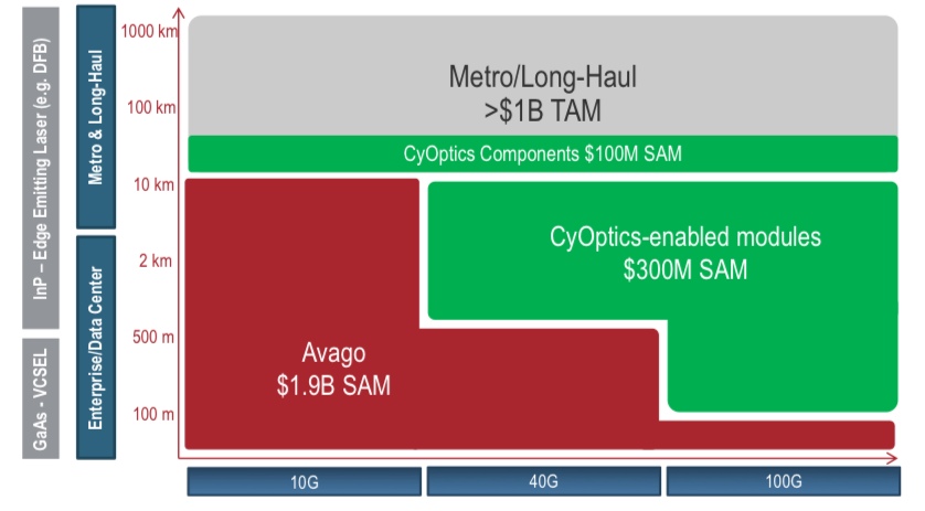 How the acquisition of CyOptics will expand Avago's market opportunities. SAM is the serviceable addressable market and TAM is the total addressable market. Source: Avago
Avago Technologies has announced its plan to acquire optical component player, CyOptics. The value of the acquisition, at US $400M, is double CyOptics' revenues in 2012.
CyOptics' sales were $210M last year, up 21 percent from the previous year. Avago's acquisition will make it the optical component industry's second largest company, behind Finisar, according to market research firm, Ovum. The deal is expected to be completed in the third quarter of the year.
The deal will add indium phosphide and planar lightwave circuit (PLC) technologies to Avago's vertical-cavity surface-emitting laser (VCSEL) and optical transceiver products. In particular, Avago will gain edge laser technology and photonic integration expertise. It will also inherit an advanced automated manufacturing site as well as entry into new markets such as passive optical networking (PON).
Avago stresses its interest in acquiring CyOptics is to bolster its data centre offerings - in particular 40 and 100 Gigabit data centre and enterprise applications - as well as benefit from the growing PON market.
The company has no plans to enter the longer distance optical transmission market beyond supplying optical components.

Significance
Ovum views the acquisition as a shift in strategy. Avago is known as a short distance interconnect supplier based on its VCSEL technology.
"Avago has seen that there are challenges being solely a short-distance supplier, and there are opportunities expanding its portfolio and strategy," says Daryl Inniss, Ovum's vice president and practice leader components.
Such opportunities include larger data centres now being built and their greater use of single-mode fibre that is becoming an attractive alternative to multi-mode as data rates and reach requirements increase.
"Avago's revenues can be lumpy partly because they have a few really large customers," says Inniss.
Another factor motivating the acquisition is that short-distance interconnect is being challenged by silicon photonics. "In the long run silicon photonics is going to win," he says.
What Avago will gain, says Inniss, is one of the best laser suppliers around. And its acquisition will impact adversely other optical module players. "CyOptics is a supplier to several transceiver vendors," says Inniss. "The outlook, two or three years' hence, is decreased business as a merchant supplier."
Inniss points out that CyOptics will represent the second laser manufacturer acquisition this year, following NeoPhotonics's acquisition of Lapis Semiconductor which has 40 Gigabit-per-second (Gbps) electro-absorption modulator lasers (EMLs).
These acquisitions will remove two merchant EML suppliers, given that CyOptics is a strong 10Gbps EML player, and lasers are a key technological asset.
See also:
For a 2011 interview with CyOptics' CEO, click here