
Scintil Photonics looks to add light to silicon
It’s the second day of Christmastide and Sylvie Menezo is working: “I enjoyed the last two days and now I’m back at work.”
But then it should not be surprising given how Menezo is both the CEO and CTO of Scintil Photonics, the French start-up that secured €4.4 million in first-round funding last year.
Origins
Scintil Photonics’ expertise is in the design of silicon photonics circuits and the addition of active III-V materials – for lasing, gain and modulation – to a silicon substrate.
The start-up is using its funding to move its technology from the lab to production, working with an unnamed commercial foundry. The firm is also growing its staff, from eight to a dozen by the year-end.
Menezo worked previously at CEA-Leti, a French technology research institute, where her roles included heading the silicon photonics lab and business development.
In her business role, there was interest from customers in Leti’s silicon photonics technology but, at the time, its III-V technology on silicon was not ready.
“There was an opportunity of putting III-V on silicon but quite a bit of investment was needed to make the technology more mature,” she says. “This is where you need quick money and a 100 per cent dedicated team.”
Menezo discussed the idea of a start-up with CEA-Leti and once the organisation was satisfied that the proposed venture could succeed, it enabled her to step down to focus solely on developing the technology.
In return, the organisation that oversees Leti, CEA Tech, took a share in the start-up before it sought funding. This is one of CEA Tech’s duties, says Menezo, to create jobs.
“Once the patent technology was strengthened, we went outside and looked for funding,” she says.
Technology
Scintil Photonics has both indium phosphide and silicon photonics expertise. The start-up’s plans to develop and sell fully photonic integrated circuits (PICs). The start-up’s optical component library includes lasers, modulators, waveguides, wavelength filters, and photodetectors.
“We have a fabrication process which is CMOS-friendly and which relies on existing silicon-photonics technology,” says Menezo. “We want to have silicon and III-V fabricated and we want to commercialise photonic ICs.”
Scintil’s work with a commercial foundry will take its technology to production using a standard silicon photonics process.
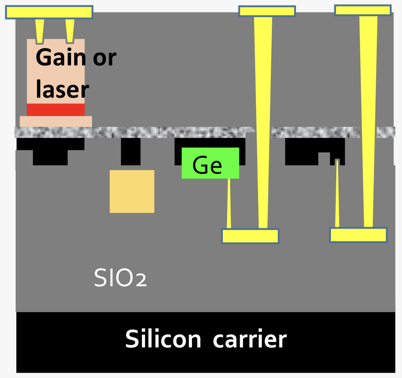
Once the silicon photonics chips are fabricated on a wafer, Scintil’s process bonds the wafer onto a silicon carrier, flips it and etches off the silicon-on-insulator (SOI) substrate.
Indium phosphide is bonded onto the exposed silicon layer before being processed to fabricate such active components as lasers, semiconductor optical amplifiers and hybrid modulators using CMOS fabrication techniques (see image).
Menezo describes the fabrication as CMOS-friendly: standard off-the-shelf processes are used while the processing of III-V is CMOS-compatible in terms of etching and electrical contacts.
Scintil’s process is also scalable, she says: new materials and functions will be added over time to the silicon photonics processes without impacting the integration of III-V materials onto the silicon.
“The more you design these devices and circuits, the more you see the design opportunities you have,” says Menezo. “This is the future if people manage to make it as a friendly as CMOS technology.”
Applications
Scintil Photonics is already working on circuit prototypes with the foundry.
The prototypes include coherent components for optical transmission and designs for 800-gigabit and 1.6-terabyte client-side interfaces. These are based on parallelising existing 400-gigabit DR4 and FR4 designs.
“For an 800-gigabit, the use of eight lanes [each lane being 100 gigabits] is indeed a good target because of [the need for] more integration,” says Menezo. “We can also scale to higher-speed lanes with our hybrid indium phosphide/ silicon photonics modulator.”
Eight-hundred gigabit modules are only needed from 2022 at the earliest.
Another application area for the technology is co-packaged optics, using optical interfaces to move data on- and off-chip.
Menezo says that the company is already thinking about the next round of funding but that it is at least two years away.

ECOC 2015: Reflections
Valery Tolstikhin, head of a design consultancy, Intengent

ECOC was a big show and included a number of satellite events, such as the 6th European Forum on Photonic Integration, the 3rd Optical Interconnect in Data Center Symposium and Market Focus, all of which I attended. So, lots of information to digest.
My focus was mainly on data centre optical interconnects and photonic integration.
Data centre interconnects
What became evident at ECOC is that 50 Gig modulation and the PAM-4 modulation format will be the basis of the next generation (after 100 Gig) data centre interconnect. This is in contrast to the current 100 Gig non-return-to-zero (NRZ) modulation using 25 Gig lanes.
This paves the way towards 200 Gig (4 x PAM-4 lanes at 25 Gig) and 400 Gig (4 x PAM-4 lanes at 50 Gig) as a continuation of quads of 4 x NRZ lanes at 25 Gig, the state-of-the-art data centre interconnect still to take off in terms of practical deployment.
The transition from 100 Gig to 400 Gig seems to be happening much faster than from 40Gig to 100 Gig. And 40 Gig serial finally seems to have gone; who needs 40 Gig when 50 Gig is available?
Another observation is that despite the common agreement that future new deployments should use single-mode fibre rather than multi-mode fibre, given the latter’s severe reach limitation that worsens with modulation speed, the multi-mode fibre camp does not give up easily.
That is because of the tons of multi-mode fibre interconnects already deployed, and the low cost of gallium arsenide 850 nm VCSELs these links use. However, the spectral efficiency of such interconnects is low, resulting in high multi-mode fibre count and the associated cost. This is a strong argument against such fibre.
Now, a short-wave WDM (SWDM) initiative is emerging as a partial solution to this problem, led by Finisar. Both OM3 and OM4 multi-mode fibre can be used, extending link spans to 100m at 25 Gig speeds.
Single mode fibre 4 x 25 Gig QSFP28 pluggables with a reach of up to 2 km, which a year ago were announced with some fanfare, seems to have become more of a commodity.
The SWDM Alliance was announced just before ECOC 2015, with major players like Finisar and Corning on board, suggesting this is a serious effort not to be ignored by the single mode fibre camp.
Lastly, single mode fibre 4 x 25 Gig QSFP28 pluggables with a reach of up to 2 km, which a year ago were announced with some fanfare, seems to have become more of a commodity. Two major varieties – PSM and WDM – are claimed and, probably shipping, by a growing number of vendors.
Since these are pluggables with fixed specs, the only difference from the customer viewpoint is price. That suggests a price war is looming, as happens in all massive markets. Since the current price still are an order of magnitude or more above the target $1/Gig set by Facebook and the like, there is still a long way to go, but the trend is clear.
This reminds me of that I’ve experienced in the PON market: a massive market addressed by a standardised product that can be assembled, at a certain time, using off-the-shelf components. Such a market creates intense competition where low-cost labour eventually wins over technology innovation.
Photonic integration
Two trends regarding photonic integration for telecom and datacom became clear at ECOC 2015.
One positive development is an emerging fabless ecosystem for photonic integrated circuits (PICs), or at least an understanding of a need for such. These activities are driven by silicon photonics which is based on the fabless model since its major idea is to leverage existing silicon manufacturing infrastructure. For example, Luxtera, the most visible silicon component vendor, is a fabless company.
There are also signs of the fabless ecosystem building up in the area of III-V photonics, primarily indium-phosphide based. The European JePPIX programme is one example. Here you see companies providing foundry and design house services emerging, while the programme itself supports access to PIC prototyping through multi-project wafer (MPW) runs for a limited fee. That’s how the ASIC business began 30 to 40 years ago.
A link to OEM customers is still a weak point, but I see this being fixed in the near future. Of course, Intengent, my design house company, does just that: links OEM customers and the foundries for customised photonic chip and PIC development.
As soon as PICs give a system advantage, which Infinera’s chips do, they become a system solution enabler, not merely ordinary components made a different way
The second, less positive development, is that photonic integration continues to struggle to find applications and markets where it will become a winner. Apart from devices like the 100 Gig coherent receiver, where phase control requirements are difficult to meet using discretes, there are few examples where photonic integration provides an edge.
Even a 4 x 25 Gig assembly using discrete components for today’s 100 Gig client side and data centre interconnect has been demonstrated by several vendors. It then becomes a matter of economies of scale and cheap labour, leaving little space for photonic integration to play. This is what happened in the PON market despite photonic integrated products being developed by my previous company, OneChip Photonics.
On a flip side, the example of Infinera shows where the power of photonic integration is: its ability to create more complicated PICs as needed without changing the technology.
One terabit receiver and transmitter chips developed by Infinera are examples of complex photonic circuits, simply undoable by means of an optical sub-assembly. As soon as PICs give a system advantage, which Infinera’s chips do, they become a system solution enabler, not merely ordinary components made a different way.
However, most of the photonic integration players - silicon photonics and indium phosphide alike - still try to do the same as what an optical sub-assembly can do, but more cheaply. This does not seem to be a winning strategy.
And a comment on silicon photonics. At ECOC 2015, I was pleased to see that, finally, there is a consensus that silicon photonics needs to aim at applications with a certain level of complexity if it is to provide any advantage to the customer.
Silicon photonics must look for more complex things, maybe 400 Gig or beyond, but the market is not there yet
For simpler circuits, there is little advantage using photonic integration, least of all silicon photonics-based ones. Where people disagree is what this threshold level of complexity is. Some suggest that 100 Gig optics for data centres is the starting point but I’m unsure. There are discrete optical sub-assemblies already on the market that will become only cheaper and cheaper. Silicon photonics must look for more complex things, maybe 400 Gig or beyond, but the market is not there yet.
One show highlight was the clear roadmap to 400 Gig and beyond, based on a very high modulation speed (50 Gig) and the PAM-4 modulation format, as discussed. These were supported at previous events, but never before have I seen the trend so clearly and universally accepted.
What surprised me, in a positive way, is that people have started to understand that silicon photonics does not automatically solve their problems, just because it has the word silicon in its name. Rather, it creates new challenges, cost efficiency being an important one. The conditions for cost efficient silicon photonics are yet to be found, but it is refreshing that only a few now believe that the silicon photonics can be superior by virtue of just being ‘silicon’.
I wouldn’t highlight one thing that I learned at the show. Basically, ECOC is an excellent opportunity to check on the course of technology development and people’s thoughts about it. And it is often better seen and felt on the exhibition floor than attending the conference’s technical sessions.
For the coming year, I will continue to track data centre interconnect optics, in all its flavours, and photonic integration, especially through a prism of the emerging fabless ecosystem.
Vishnu Shukla, distinguished member technical staff in Verizon’s network planning group.
There were more contributions related to software-defined networking (SDN) and multi-layer transport at ECOC. There were no new technology breakthroughs as much as many incremental evolutions to high-speed optical networking technologies like modulation, digital signal processors and filtering.
I intend to track technologies and test results related to transport layer virtualisation and similar efforts for 400 Gig-and-beyond transport.
Vladimir Kozlov, CEO and founder of LightCounting
I had not attended ECOC since 2000. It is a good event, a scaled down version of OFC but just as productive. What surprised me is how small this industry is even 15 years after the bubble. Everything is bigger in the US, including cars, homes and tradeshows. Looking at our industry on the European scale helps to grasp how small it really is.
What is the next market opportunity for optics? The data centre market is pretty clear now, but what next?
Listening to the plenary talk of Sir David Paine, it struck me how infinite technology is. It is so easy to get overexcited with the possibilities, but very few of the technological advances lead to commercial success.
The market is very selective and it takes a lot of determination to get things done. How do start-ups handle this risk? Do people get delusional with their ideas and impact on the world? I suspect that some degree of delusion is necessary to deal with the risks.
As for issues to track in the coming year, what is the next market opportunity for optics? The data centre market is pretty clear now, but what next?
OneChip Photonics targets the data centre with its PICs
OneChip Photonics is developing integrated optical components for the IEEE 40GBASE-LR4 and 100GBASE-LR4 interface standards.
The company believes its photonic integrated circuits (PICs) will more than halve the cost of the 40 and 100 Gigabit 10km-reach interfaces, enough for LR4 to cost-competitively address shorter reach applications in the data centre.

"I think we can cut the price [of LR4 modules] by half or better”
Andy Weirich, OneChip Photonics
The products mark an expansion of the Canadian startup's offerings. Until now OneChip has concentrated on bringing PIC-based passive optical network (PON) transceivers to market.
LR4 PICs
The startup is developing separate LR4 transmitter and receiver PICs. The 40 and 100GBASE-LR4 receivers are due in the third quarter of 2012, while the transmitters are expected by the year end.
The 40GBASE-LR4 receiver comprises a wavelength demultiplexer - a 4-channel arrayed waveguide grating (AWG) - and four photo-detectors operating around 1300nm. A spot-size converter - an integrated lens - couples the receiver's waveguide's mode field to the connecting fibre.
"[Data centre operators] are saying that they are having to significantly bend out of shape their data centre architecture to accommodate even 300m reaches”
The 40GBASE-LR4 transmitter PIC comprises four directly-modulated distributed feedback (DFB) lasers while the 100GBASE-LR4 use four electro-absorption modulator DFB lasers. Different lasers for the two PICs are required since the four wavelengths at 100 Gig, also around 1300nm, are more tightly spaced: 5nm versus 20nm. "They are much closer together than the 40 Gig version,” says Andy Weirich, OneChip Photonics' vice president of product line management.
Another consequence of the wider wavelength spacings is that the 40 Gig transmitter uses four discrete lasers. “Because the 40 Gig wavelengths are much further apart, putting all the lasers on the one die is problematic," says Weirich. The 40GBASE-LR4 design thus uses five indium phosphide components: four lasers and the AWG, while the 40GBASE-LR4 receiver and the two 100GBASE-LR4 devices are all monolithic PICs.
Both LR4 transmitter designs also include monitor photo-diodes for laser control
Lower size and cost
OneChip says the resulting PICs are tiny, measuring less than 3mm in length. “We think the PICs will enable the packaging of LR4 in a QSFP,” says Weirich. 40GBASE-LR4 products already exists in the QSFP form factor but the 100GBASE-LR4 uses a CFP module.
The startup expects module makers to use its receiver chips once they become available rather than wait for the receiver-transmitter PIC pair. "Reducing the size of one half the solution is possibly good enough to fit the whole hybrid design - the PIC for the receive and discretes for the transmit - into a QSFP,” says Weirich.
The PICs are expected to reduce significantly the cost of LR4 modules. "I think we can cut the price by half or better,” says Weirich. “Right now the LR4 is far too expensive to be used for data centre interconnect.” OneChip expects its LR4 PICs to be cost-competitive with the 2km reach 10x10 MSA interface.
Meanwhile, short-reach 40 and 100 Gig interfaces use VCSEL technology and multi-mode fibre to address 100m reach requirements. In larger data centres this reach is limiting. Extended reach - 300-400m - multimode interfaces have emerged but so far these are at 40 Gig only.
"[Data centre operators] are saying that they are having to significantly bend out of shape their data centre architecture to accommodate even 300m reaches,” says Weirich. “They really want more than that.”
OneChip believes interfaces distances of 200m-2km is underserved and it is this market opportunity that it is seeking to address with its LR4 designs.
Roadmap
Will OneChip integrate the design further to product a single PIC LR4 transceiver?
"It can be put into one chip but it is not clear that there is an economic advantage,” says Weirich. Indeed one PIC might even be more costly than the two-PIC chipset.
Another factor is that at 100 Gig, the 25Gbps electronics present a considerable signal integrity design challenge. “It is very important to keep the electronics very close to the photo-detectors and the modulators,” he says. “That becomes more difficult if you put it all on the one chip.” The fabrication yield of a larger single PIC would also be reduced, impacting cost.
OneChip, meanwhile, has started limited production of its PON optical network unit (ONU) transceivers based on its EPON and GPON PICs. The company's EPON transceivers are becoming generally available while the GPON transceivers are due in two months’ time.
The company has yet to decide whether it will make its own LR4 optical modules. For now OneChip is solely an LR4 component supplier.
Further reading:
See OFC/ NFOEC 2012 highlights, the Kotura story in the Optical Engines section
OFC/NFOEC 2012 industry reflections - Part 1
The recent OFC/NFOEC show, held in Los Angeles, had a strong vendor presence. Gazettabyte spoke with Infinera's Dave Welch, chief strategy officer and executive vice president, about his impressions of the show, capacity challenges facing the industry, and the importance of the company's photonic integrated circuit technology in light of recent competitor announcements.
OFC/NFOEC reflections: Part 1

"I need as much fibre capacity as I can get, but I also need reach"
Dave Welch, Infinera
Dave Welch values shows such as OFC/NFOEC: "I view the show's benefit as everyone getting together in one place and hearing the same chatter." This helps identify areas of consensus and subjects where there is less agreement.
And while there were no significant surprises at the show, it did highlight several shifts in how the network is evolving, he says.
"The first [shift] is the realisation that the layers are going to physically converge; the architectural layers may still exist but they are going to sit within a box as opposed to multiple boxes," says Welch.
The implementation of this started with the convergence of the Optical Transport Network (OTN) and dense wavelength division multiplexing (DWDM) layers, and the efficiencies that brings to the network.
That is a big deal, says Welch.
Optical designers have long been making transponders for optical transport. But now the transponder isn't an element in the integrated OTN-DWDM layer, rather it is the transceiver. "Even that subtlety means quite a bit," say Welch. "It means that my metrics are no longer 'gray optics in, long-haul optics out', it is 'switch-fabric to fibre'."
Infinera has its own OTN-DWDM platform convergence with the DTN-X platform, and the trend was reaffirmed at the show by the likes of Huawei and Ciena, says Welch: "Everyone is talking about that integration."
The second layer integration stage involves multi-protocol label switching (MPLS). Instead of transponder point-to-point technology, what is being considered is a common platform with an optical management layer, an OTN layer and, in future, an MPLS layer.
"The drive for that box is that you can't continue to scale the network in terms of bandwidth, power and cost by taking each layer as a silo and reducing it down," says Welch. "You have to gain benefits across silos for the scaling to keep up with bandwidth and economic demands."
Super-channels
Optical transport has always been about increasing the data rates carried over wavelengths. At 100 Gigabit-per-second (Gbps), however, companies now use one or two wavelengths - carriers - onto which data is encoded. As vendors look to the next generation of line-side optical transport, what follows 100Gbps, the use of multiple carriers - super-channels - will continue and this was another show trend.
Infinera's technology uses a 500Gbps super-channel based on dual polarisation, quadrature phase-shift keying (DP-QPSK). The company's transmit and receive photonic integrated circuit pair comprise 10 wavelengths (two 50Gbps carriers per 50GHz band).
Ciena and Alcatel-Lucent detailed their next-generation ASICs at OFC. These chips, to appear later this year, include higher-order modulation schemes such as 16-QAM (quadrature amplitude modulation) which can be carried over multiple wavelengths. Going from DP-QPSK to 16-QAM doubles the data rate of a carrier from 100Gbps to 200Gbps, using two carriers each at 16-QAM, enables the two vendors to deliver 400Gbps.
"The concept of this all having to sit on one wavelength is going by the wayside," say Welch.
Capacity challenges
"Over the next five years there are some difficult trends we are going to have to deal with, where there aren't technical solutions," says Welch.
The industry is already talking about fibre capacities of 24 Terabit using coherent technology. Greater capacity is also starting to be traded with reach. "A lot of the higher QAM rate coherent doesn't go very far," says Welch. "16-QAM in true applications is probably a 500km technology."
This is new for the industry. In the past a 10Gbps service could be scaled to 800 Gigabit system using 80 DWDM wavelengths. The same applies to 100Gbps which scales to 8 Terabit.
"I'm used to having high-capacity services and I'm used to having 80 of them, maybe 50 of them," says Welch. "When I get to a Terabit service - not that far out - we haven't come up with a technology that allows the fibre plant to go to 50-100 Terabit."
This issue is already leading to fundamental research looking at techniques to boost the capacity of fibre.
PICs
However, in the shorter term, the smarts to enable high-speed transmission and higher capacity over the fibre are coming from the next-generation DSP-ASICs.
Is Infinera's monolithic integration expertise, with its 500 Gigabit PIC, becoming a less important element of system design?
"PICs have a greater differentiation now than they did then," says Welch.
Unlike Infinera's 500Gbps super-channel, the recently announced ASICs use two carriers and 16-QAM to deliver 400Gbps. But the issue is the reach that can be achieved with 16-QAM: "The difference is 16-QAM doesn't satisfy any long-haul applications," says Welch.
Infinera argues that a fairer comparison with its 500Gbps PIC is dual-carrier QPSK, each carrier at 100Gbps. Once the ASIC and optics deliver 400Gbps using 16-QAM, it is no longer a valid comparison because of reach, he says.
Three parameters must be considered here, says Welch: dollars/Gigabit, reach and fibre capacity. "I have to satisfy all three for my application," he says.
Long-haul operators are extremely sensitive to fibre capacity. "I need as much fibre capacity as I can get," he says. "But I also need reach."
In data centre applications, for example, reach is becoming an issue. "For the data centre there are fewer on and off ramps and I need to ship truly massive amounts of data from one end of the country to the other, or one end of Europe to the other."
The lower reach of 16-QAM is suited to the metro but Welch argues that is one segment that doesn't need the highest capacity but rather lower cost. Here 16-QAM does reduce cost by delivering more bandwidth from the same hardware.
Meanwhile, Infinera is working on its next-generation PIC that will deliver a Terabit super-channel using DP-QPSK, says Welch. The PIC and the accompanying next-generation ASIC will likely appear in the next two years.
Such a 1 Terabit PIC will reduce the cost of optics further but it remains to be seen how Infinera will increase the overall fibre capacity beyond its current 80x100Gbps. The integrated PIC will double the 100Gbps wavelengths that will make up the super-channel, increasing the long-haul line card density and benefiting the dollars/ Gigabit and reach metrics.
In part two, ADVA Optical Networking, Ciena, Cisco Systems and market research firm Ovum reflect on OFC/NFOEC. Click here
Terabit Consortium embraces OFDM
 “This project is very challenging and very important”
Shai Stein, Tera Santa Consortium
Given the continual growth in IP traffic, higher-speed light paths are going to be needed, says Shai Stein, chairman of the Tera Santa Consortium and ECI Telecom’s CTO: “If 100 Gigabit is starting to be deployed, within five years we’ll start to see links with tenfold that capacity, meaning one Terabit.”
The project is funded by the seven participating firms and the Israeli Government. According to Stern, the Government has invested little in optical projects in recent years. “When we look at the [Israeli] academies and industry capabilities in optical, there is no justification for this,” says Stern. “We went with this initiative in order to get Government funding for something very challenging that will position us in a totally different place worldwide.”
Orthogonal frequency division multiplexing
OFDM differs from traditional dense wavelength division multiplexing (DWDM) technology in how fibre bandwidth is used. Rather than sending all the information on a lightpath within a single 50 or 100GHz channel – dubbed single-carrier transmission – OFDM uses multiple narrow carriers. “Instead of using the whole bandwidth in one bulk and transmitting the information over it, [with OFDM] you divide the spectrum into pieces and on each you transmit a portion of the data,” says Stein. “Each sub-carrier is very narrow and the summation of all of them is the transmission.”
“Each time there is a new arena in telecom we find that there is a battle between single carrier modulation and OFDM; VDSL began as single carrier and later moved to OFDM,” says Amitai Melamed, involved in the project and a member of ECI’s CTO office. “In the optical domain, before running to [use] single-carrier modulation as is currently done at 100 Gigabit, it is better to look at the OFDM domain in detail rather than jump at single-carrier modulation and question whether this was the right choice in future.”
OFDM delivers several benefits, says Stern, especially in the flexibility it brings in managing spectrum. OFDM allows a fibre’s spectrum band to be used right up to its edge. Indeed Melamed is confident that by adopting OFDM for optical, the spectrum efficiency achieved will eventually match that of wireless.
“OFDM is very tolerant to rate adaptation.”
Amitai Melamed, ECI Telecom
The technology also lends itself to parallel processing. “Each of the sub-carriers is orthogonal and in a way independent,” says Stern. “You can use multiple small machines to process the whole traffic instead of a single engine that processes it all.” With OFDM, chromatic dispersion is also reduced because each sub-carrier is narrow in the frequency domain.
Using OFDM, the modulation scheme used per sub-carrier can vary depending on channel conditions. This delivers a flexibility absent from existing single-carrier modulation schemes such as quadrature phase-shift keying (QPSK) that is used across all the channel bandwidth at 100 Gigabit-per-second (Gbps). “With OFDM, some of the bins [sub-carriers] could be QPSK but others could be 16-QAM or even more,” says Melamed.
The approach enables the concept of an adaptive transponder. “I don’t always need to handle fibre as a time-division multiplexed link – either you have all the capacity or nothing,” says Melamed. “We are trying to push this resource to be more tolerant to the media: We can sense the channels' and adapt the receiver to the real capacity.” Such an approach better suits the characteristics of packet traffic in general he says: “OFDM is very tolerant to rate adaptation.”
The Consortium’s goal is to deliver a 1 Terabit light path in a 175GHz channel. At present 160, 40Gbps can be crammed within the a fibre's C-band, equating to 6.4Tbps using 25GHz channels. At 100Gbps, 80 channels - or 8Tbps - is possible using 50GHz channels. A 175GHz channel spacing at 1Tbps would result in 23Tbps overall capacity. However this figure is likely to be reduced in practice since frequency guard-bands between channels are needed. The spectrum spacings at speeds greater than 100Gbps are still being worked out as part of ITU work on "gridless" channels (see OFC announcements and market trends story).
ECI stresses that fibre capacity is only one aspect of performance, however, and that at 1Tbps the optical reach achieved is reduced compared to transmissions at 100Gbps. “It is not just about having more Gigabit-per-second-per-Hertz but how we utilize the resource,” says Melamed. “A system with an adaptive rate optimises the resource in terms of how capacity is managed.” For example if there is no need for a 1Tbps link at a certain time of the day, the system can revert to a lower speed and use the spectrum freed up for other services. Such a concept will enable the DWDM system to be adaptive in capacity, time and reach.
Project focus
The project is split between digital and analogue, optical development work. The digital part concerns OFDM and how the signals are processed in a modular way.
The analogue work involves overcoming several challenges, says Stern. One is designing and building the optical functions needed for modulation and demodulation with the accuracy required for OFDM. Another is achieving a compact design that fits within an optical transceiver. Dividing the 1Tbps signal into several sub-bands will require optical components to be implemented as a photonic integrated circuit (PIC). The PIC will integrate arrays of components for sub-band processing and will be needed to achieve the required cost, space and power consumption targets.
Taking part in the project are seven Israeli companies - ECI Telecom, the Israeli subsidiary of Finisar, MultiPhy, Civcom, Orckit-Corrigent, Elisra-Elbit and Optiway- as well as five Israeli universities.
 Two of the companies in the Consortium
“There are three types of companies,” says Stern. “Companies at the component level – digital components like digital signal processors and analogue optical components, sub-systems such as transceivers, and system companies that have platforms and a network view of the whole concept.”
The project goal is to provide the technology enablers to build a terabit-enabled optical network. A simple prototype will be built to check the concepts and the algorithms before proceeding to the full 1Terabit proof-of-concept, says Stern. The five Israeli universities will provide a dozen research groups covering issues such as PIC design and digital signal processing algorithms.
Any intellectual property resulting from the project is owned by the company that generates it although it will be made available to any other interested Consortium partner for licensing.
Project definition work, architectures and simulation work have already started. The project will take between 3-5 years but it has a deadline after three years when the Consortium will need to demonstrate the project's achievements. “If the achievements justify continuation I believe we will get it [a funding extension],” says Stern. “But we have a lot to do to get to this milestone after three years.
Project funding for the three years is around US $25M, with the Israeli Office of the Chief Scientist (OCS) providing 50 million NIS (US $14.5M) via the Magnet programme, which ECI says is “over half” of the overall funding.
Further reading:
u2t Photonics: Adapting to a changing marketplace
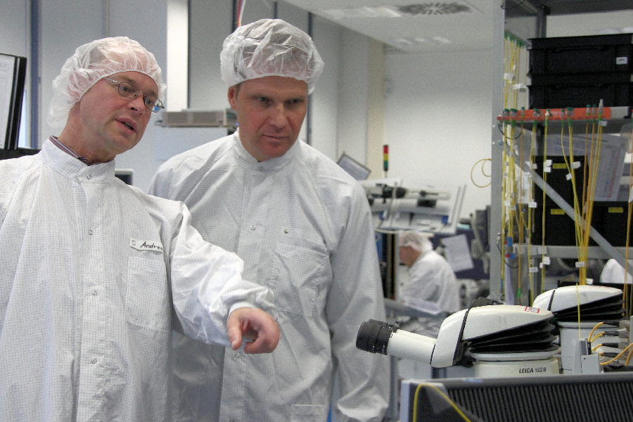
 u2t Photonics' Jens Fiedler, vice president sales and marketing (left), and CEO Andreas Umbach.
u2t Photonics has begun sampling its second-generation coherent receiver module. The dual-polarisation, quadrature phase-shift keying (DP-QPSK) coherent transmission receiver adds polarisation diversity to the company’s first-generation design – an indium-phosphide 90O hybrid design that includes balanced photo-detectors – all within an integrated module. u2t Photonics has developed two such coherent receiver designs, to address the 40 Gigabit-per-second (Gbps) and the 100Gbps markets, adding to the company’s first-generation design now available in small volumes.
“We can explore [next-gen coherent] solutions before we need them and we learn a lot from these partnerships” Andreas Umbach
The latest coherent receiver design represents what CEO Andreas Umbach believes u2t Photonics does best: using its radio frequency (RF) and optical component expertise to design high-speed integrated optical receiver modules.
Differentiation at 100 Gigabit
u2t Photonics is a leading component supplier for the 40 Gigabit market with its photo-detectors and more recently differential phase-shift keying (DPSK) integrated receiver designs that combine a delay-line interferometer with a balanced receiver. Such receivers are used for optical transponder and line card designs. Now, with its latest integrated coherent receiver, the German company aims to exploit the emerging 100 Gigabit market.
“The 40 Gig market will be strong for awhile yet, but 100 Gig is coming and will start to squeeze 40 Gig,” says Umbach. “Right now we do not see 100 Gig cannibalising 40 Gig,” says Jens Fiedler, vice president sales and marketing at u2t Photonics. “For DP-QPSK, 100 Gig might cannibalise 40 Gig since the technology for 40 Gig does not offer a big cost benefit for the customer.”
The emergence of 100 Gigabit optical links and its use of more advanced modulation have changed component requirements. Whereas the DPSK modulation scheme for 40Gbps requires photo-detectors with bandwidths that match the data rate, 100Gbps coherent requires photo-detectors with bandwidths of 28GHz only.
“In principle, not having the requirement of a very high-speed photo-detector makes it [100Gbps] a little bit easier, yet having 40 Gig serial is not unique anymore; there are differences in performance but it is not a limiting factor,” says Umbach.
Instead what matters for optical component players is to understand the 100Gbps functional requirements and deliver a design that meets them as early as possible, says Umbach. The challenges after that are scaling volume production and driving down cost. “We are the first company with a second generation design, offering the highest integration based on the [100G OIF] standard,” says Fiedler. “No doubt our competition is tough, but so far we are doing pretty well.”
u2t Photonics dismisses the view that the advent of high-speed CMOS ASICs that execute digital signal processing algorithms at the DP-QPSK receiver is eroding the need for the company’s expertise by enabling less specialist optics to be used. The optical specification requirements the company faces are challenging enough because customers still want to get the best performance from the links, it says.
"u2t Photonics has grown its revenue tenfold in the last five years" Jens Fiedler
“The challenge for us now is not just a photo-detector with a higher bandwidth but a coherent receiver that can detect the polarisation, phase and amplitude of the optical signal,” says Umbach. “That puts a much higher challenge on the components – not just high speed and efficiency but linearity in all these parameters.”
EC Galactico and Mirthe projects
To keep on top of next-generation coherent optical transmission schemes, u2t Photonics is a member of two European Commission (EC) Framework 7 projects dubbed Galactico (Blending diverse photonics and electronics on silicon for integrated and fully functional coherent Tb Ethernet) and Mirthe (Monolithic InP-based dual polarization QPSK integrated receiver and transmitter for coherent 100-400Gb Ethernet).
The Galactico project, which includes Nokia Siemens Networks, will develop photonic integrated circuits (PICS) that will implement a 100Gbps DP-QPSK coherent transmitter and receiver, a 600Gbps dense wavelength division multiplexing (DWDM) DP-QPSK coherent transmitter and receiver and a 280Gbps DP-128 quadrature amplitude modulation (QAM) transmitter that will deliver 10bit/sec/Hz spectral efficiency. The second project, Mirthe, is tasked with developing multi-level coding schemes using QPSK and QAM.
“Both projects address next generation [high-speed optical transmission] and the next level of integration of coherent receivers and transmitters for complex coherent systems,” says Umbach.
u2t is working with the projects’ partners in defining the devices needed for next-generation networks. In particular it is helping define the specifications needed for the ICs to drive such optical devices as well as what the product should look like to aid integration and packaging. “We have partners in the Mirthe project such as the Heinrich Hertz Institute and [Alcatel Thales] III V Lab that are focusing on chip design according to our requirements and matching our packaging development efforts,” says Umbach. The Galactico project is similar but here u2t Photonics is also contributing its integrated modulator technology for more complex transmission formants compared to the current DP-QPSK.
The company says its involvement in these projects is less to do with the research funding made available. Rather, it is the chance to work with partners on the R&D side. “We can explore solutions before we need them and we learn a lot from these partnerships,” says Umbach.
Changing markets
The emergence of three or four dominant module makers as the optical market matures presents new challenges for u2t Photonics. These emerging leaders are increasingly vertically integrated, using their own in-house components within their modules.
“Vertical integration is something we have to face and are fully aware of,” says Fiedler. To remain a valid component supplier, what matters is delivering component performance, volume capability, and cost that meet customer targets and challenge their own developments. “That is what we need to – at least be the second source for these vertical integrated companies,” says Fiedler.
Umbach points out that many of the system vendors are developing their own 100Gbps systems on line cards, and this represents another market opportunity for u2t Photonics, independent of the module makers.
“u2t might not offer the best pricing and might have issues - technical challenges common when you have early, leading-edge components,” says Fiedler. “But finally u2t is chosen as the supplier. They know we deliver the products.” To prove his point, Fiedler claims u2t Photonics has grown its revenue tenfold in the last five years.
Europe’s optical vendors
The last few years has seen significant consolidation among European optical component firms. Whereas Europe has system vendors that include Alcatel-Lucent, Nokia Siemens Networks, Ericsson, ADVA Optical Networking and Transmode Systems, the number of component vendors has continued to shrink. Bookham became a US company before merging with Avanex to become Oclaro, MergeOptics folded and its assets were acquired by FCI, while CoreOptics was acquired by Cisco Systems in May 2010.
Oclaro may be a US-registered company but its main operations are in China and Europe, points out Umbach. And many companies’ operations in the US and elsewhere have large headcounts in the Far East such that they could be view as more Asian companies, he adds.
“I believe there are lot of systems and components expertise in Europe - in Italy, the UK and Germany,” says Umbach. “Maybe they are just teams out of global players, like the CoreOptics team which will stay in Nuremberg although it is now a US company.” u2t Photonics itself has opened a unit in the UK. “We don’t feel too lonely,” he adds. “There is a lot of know-how we can look at here in these areas, not only other companies but academia in all the photonics fields.”
In turn, the market is a global one, says the firm, with the Chinese market being particular important with its large 40Gbps DPSK deployments and the importance of Huawei as a leading system vendor. Fiedler says the Chinese market is rapidly moving and has the potential to be a huge market for high-speed optical transmission. Yet despite emerging Chinese optical component players, the likes of Huawei are no different to other system vendors in terms of the criteria used when choosing optical components: performance capabilities and cost.
u2t Photonics remains open to all developments. “We have the opportunity to grow and expand our own business, and face the challenge with our bigger competitors,” says Umbach. “And if there is a reasonable path into consolidation, there is nothing that keeps us from going this way.”
Further information:
A presentation on Galactico, click here
A presentation on Mirthe, click here
Infinera PICs 100Gbps coherent
Infinera is expediting its product plans, basing its optical transmission roadmap on coherent detection.
The company plans to launch a 100Gbps coherent transmission system in 2012. The design will be based on a pair of 5x100Gbps ultra-long-haul photonic integrated circuit (PIC) chips that will enable its systems to deliver 8 Terabits-per-second (Tbps) over a fibre.

“This change in roadmap is because of the successful development of our 100G coherent ASIC programme, and we have integrated five 100Gbps coherent channels onto one card.”
Drew Perkins, Infinera
Infinera also announced that it will be adding 40Gbps coherent detection to its DTN system in 2011. The 40Gbps will be based on optical modules and not its PIC technology. Using its planar technology and working with optical module suppliers to integrate its in-house coherent technology, Infinera’s DTN system will support 25GHz channel spacings to cram 160 lightpaths across the C-band, to deliver 6.4Tbps capacity.
Why is the announcement important?
Infinera had still to launch its 10x40Gbps PIC. This announcement marks a shift in Infinera’s strategy to focus on 100Gbps and gain a technology edge by offering the highest line speed at an unmatched density.
“It’s a good roadmap for Infinera,” says Jimmy Yu, a director at the Dell'Oro Group. “From an optical market perspective, I think 2012 is the right time for having a 100Gbps DWDM long-haul system. And it'll definitely be coherent.”
Dell’Oro expects to see early adopters of 100Gbps in 2010 and 2011, but it will be 2012/2013 when the market for 100Gbps will ramp.
What has motivated Infinera’s shift has been its success in developing coherent technology, says Drew Perkins, Infinera’s CTO. Coherent technology in combination with PICs is the best of all worlds, he says, marrying the two most significant optical developments of the last decade.
Perkins admits Infinera has been slow in offering 40Gbps technology.
“We are late to a very small market,” he says. “We think there is a 40G squeeze going on – it took the industry so long to get 40Gbps right with coherent technology such that 100Gbps is now just around the corner, as we are proving here.”
Yet Infinera will offer 40Gbps next year and will seek to differentiate itself with 25GHz channel spacing. “But it [the 40Gbps design] will be rapidly superseded by our 100Gbps, 8Tbps technology and then we believe we will be early to market with 100Gbps,” says Perkins.
Dell’Oro says 40Gbps is growing rapidly and it expects continued growing. “In 2009, 40Gbps wavelength shipments grew a little over 160 percent, and we’re forecasting it to grow nearly 90 percent in 2010,” says Yu. “If Infinera delivers 40Gbps on 25GHz channel spacing, it'll be a good interim step to 100Gbps.”
What’s being done?
Infinera has now scrapped its 10x40Gbps differential quadrature phase-shift keying (DQPSK) PIC, going to a 5x100Gbps polarisation multiplexing quadrature phase-shift keying (PM-QPSK) design instead. Interestingly, Perkins says that the 10x40Gbps transmitter PIC was designed from the start to also support 5x100Gbps PM-QPSK modulation.
The challenge is designing the coherent receiver PIC which is significantly different, and has required Infinera to gain coherent expertise in-house.
The receiver PIC also requires a local oscillator laser. “We have integrated the laser onto the receiver PIC per channel,” says Perkins. Infinera’s PICs already use lasers that are tuned over a significant number of channels though not the whole C-band so this is using technology it already has.
Another key aspect of the coherent receiver is the associated electronics that comprises very high-speed A/D converters, a digital signal processor and most likely advanced forward error correction. Developing such an ASIC is a significant challenge.
Is Infinera developing such a design? Infinera points to its Ottawa, Ontario-based research facility that was announced in September last year. “That team is working on ASIC level coherent technology,” says Perkins. “This change in roadmap is because of the successful development of our 100G coherent ASIC programme, and we have integrated five 100Gbps coherent channels onto one card.”
Did Infinera consider designing a 10x100Gbps PIC? “It comes down to the size of the line card,” says Perkins. Infinera believes the resulting terabit line card would have been too large a jump for the industry given the status of associated electronics such as switching technology.
What next?
Infinera says that in 2012 it will ship systems based on its 100Gbps coherent PICs to customers but it is unwilling to detail the key development milestones involved between now and then.
As for future product developments, Infinera claims it can extend overall capacity of its coherent technology in several directions.
It says it can integrate 10, 100Gbps channels onto a PIC. “Somewhere in the future we undoubtedly will”, says Perkins. The company also states that in the “fullness of time” it could deliver 100Gbps over 25GHz channel spacings.
Perkins also reconfirmed that Infinera will continue to advance the modulation scheme used, going from QPSK to include higher order quadrature amplitude modulation (QAM) schemes.
Photonic integration: Bent on disruption
“This is a general rule: what starts as a series of parts loosely strung together, if used heavily enough, congeals into a self-contained unit.”
W. Brian Arthur, The Nature of Technology
Infinera's Dave Welch: PICs are fibre-optic's current disruption
Dave Welch likes to draw a parallel with digital photography when discussing the use of photonic integration for optical networking. “The CMOS photodiode array – a photonic integrated circuit - changed the entire supply chain of photography,” says Welch, the chief strategy officer at Infinera.
Applied to networking, the photonic integrated circuit (PIC) is similar, argues Welch. It benefits system cost by integrating individual optical components but it delivers more. “All the value – inherently harder to pin down - of networking efficiency of a system that isn’t transponder-based,” says Welch.
Just how disruptive a technology the PIC proves to be is unclear but there is no doubting the growing role of optical integration.
“Integration is a key part of our thinking,” says Sam Bucci, vice president, WDM, Alcatel-Lucent’s optics activities. When designing a new platform, Alcatel-Lucent surveys components and techniques to identify disruptive technologies. Even if it chooses to implement functions using discrete components, the system is designed taking into account future integrated implementations.
“We are seeing interest [in photonic integration] across the spectrum," says Stefan Rochus, vice president of marketing and business development at CyOptics. "Long-haul, metro, access and chip-to-chip - everything is in play."
The drivers for optical integration’s greater use are harder to pin down.
Operators must contend with yearly data traffic growth estimated at between 45 to 65 percent yet their revenues are growing modestly. “It’s no secret that the capacity curve - whether the line side or the client side - is growing at an astonishing clip,” says Bucci.
The onus is thus on equipment and component makers to deliver platforms that reduce the transport cost per bit."Delivering more for less," says Graeme Maxwell, vice president of hybrid integration at CIP Technologies. “Space is a premium, power is an issue, operators want performance maintained or improved – all are driving integration.”
Cost is an issue for optical components with yearly price drops of 20 percent being common. “Hitting the cost-curve, we have run out of ways to do that with classic optics,” says Sinclair Vass, commercial director, EMEA at JDS Uniphase.
High-speed optical transmission at 40 and 100 Gigabit per second (Gbps) requires photonic integration though here the issues are as much performance as cost reduction. Indeed, its use can be viewed as the result of the integration between electronics and optics. To address optical signal impairments, chips must work at the edge of their performance, requiring the optical signal to be split into slower, parallel streams. Such an arrangement is ripe for photonic integration.
“It is as if there are two kinds of integration: at the boundary between optics and electronics, and the purely optical planar waveguide stuff,” says Karen Liu, vice president, components and video technologies at market research firm Ovum.
The other market where the full arsenal of optical integration techniques – hybrid and monolithic integration – is being applied is optical transceivers for passive optical networking (PON). Here the sole story is cost.
As old as the integrated circuit
Photonic integration is not new. The idea was first mooted in a 1969 AT&T Bell Labs’ paper that described how multiple miniature optical components could be interconnected via optical waveguides made using thin-film dielectric materials. But so far industry adoption for optical networking has been limited.

"Two kinds of integration: at the boundary between optics and electronics, and the purely optical planar waveguide stuff"
Karen Liu, Ovum
Heavy Reading, in a 2008 report, highlighted the limited progress made in photonic integration in recent years, with the exception of Infinera, a maker of systems based on a dense wavelength division multiplexing (DWDM) 10x10Gbps monolithically integrated PIC.
“Infinera has held very consistently to its original story, including sub-wavelength grooming, and have made progress over time,” says Liu. But she points out a real disruptive impact has not yet been seen: “The problem with the digital camera analogy is that something that is disruptive is not a straight replacement but implies the next step: changing the network architecture, not just how a system is implemented.”
On-off keying to phase modulation
One way operators are accommodating traffic growth is cramming more data down a fibre. It is this trend- from 10Gbps to 40 and 100Gbps lightpaths - that is spurring photonic integration.
“If you look at current 100 Gigabit, it is a bigger configuration than we would like,” says Joe Berthold, Ciena’s vice president of network architecture. Ciena’s first 100Gbps design requires three line cards, taking five inches of rack space, while its second-generation design will fit on a single, two-inch card.
Both 40 and 100Gbps transmissions must also operate over existing networks, matching the optical link performance of 10Gbps despite dispersion being more acute at higher line speeds. To meet the challenge, the industry has changed how it modulates data onto light. Whereas previous speed increments up to 10Gbps used simple on-off keying, 40 and 100Gbps use advanced modulation schemes based on phase, or phase combined with polarisation.
The modulation schemes split the optical signal into parallel paths to lower symbol rates. For example, 40Gbps differential quadrature phase-shift keying (DQPSK) uses two signals that effectively operating at 20 Gigabaud. Halving the rate relaxes the high-speed electronics requirements at the expense of complicating the optical circuitry.
The concept is extended further at 100Gbps. Here polarisation is combined with phase modulation (either DQPSK, or QPSK if coherent detection is used) such that four signals are used in parallel, each operating at 28 Gigabaud.

“The 40/100G area is shaping up to be the equivalent of breaking the sound barrier”
Brad Smith, LightCounting
“Optical integration is becoming a necessity because of 40 and 100 Gigabit [transmission],” says Berthold. “The modulation formats require you to deal with signals in parallel, and using non-integrated components explodes the complexity.”
The Optical Internetworking Forum organisation has chosen dual-polarisation QPSK (DP- QPSK) as the favoured modulation scheme for 100Gbps and has provided integrated transmitter and receiver module guidelines to encourage industry convergence on common components. In contrast, for 40Gbps several designs have evolved: differential phase-shift keying (DPSK) through to DQPSK and DP-QPSK.
Kim Roberts, Nortel's director of optics research, while acknowledging that optical integration benefits system footprint and cost, downplays its overall significance.
For him, the adoption of coherent systems for 40 and 100Gbps – Nortel was first to market with a 40Gbps DP-QPSK system – move the complexity ‘into CMOS’, leaving optics to perform the basic functions. “I don’t see an overwhelming argument for integration,” says Roberts. “It’s useful and shows up in lower cost and smaller designs but it’s not a revolution.”
Meanwhile, optical component companies are responding by integrating various building blocks to address the bulkier 40 and 100Gbps designs.
NeoPhotonics is now shipping two PICs for 40 and 100Gbps receivers: a DQPSK demodulator based on two delay-line interferometers (DLIs) and a coherent mixer for a DP-QPSK receiver.
The DLI, as implied by the name, delays one of the received symbols and compares it with the adjacent received one to uncover the phase-encoded information. This is then fed to a balanced detector - a photo-detector pair. For DQPSK, either two DLIs or a single DLI plus 90-degree hybrid are required along with two balanced receivers.
For 100Gbps, a DP-QPSK receiver has four channels - a polarisation beam splitter separates the two polarisations and each component is mixed with a component from a local reference signal using a 90-degree hybrid mixer. The two hybrid mixers decompose the referenced phase to intensity outputs representing the orthogonal phase components of the signal and the four differential outputs are fed into the four balanced detectors (Click here for OIF document and see Fig 5).
Neophotonics’ coherent mixer integrates monolithically all the demodulation functions between the polarisation beam splitter and the balanced photo-detectors.
The company has both indium phosphide and planar lightwave circuit (PLC) technology integration expertise but chose to implement its designs using PLC technology. “Indium phosphide is good for actives but is not good for passives and it is very expensive,” says Ferris Lipscomb, vice president of marketing at NeoPhotonics.
One benefit of using PLC for demodulation is that the signal path lengths need to have sub-millimeter accuracy to recover phase; implementing a discrete design using fibre to achieve such accuracy is clearly cumbersome.
Another development that reduces size and cost involves the teaming of u2t Photonics, a high-speed photo-detector and indium phosphide specialist, with Optoplex and Kylia, free-space optics DLI suppliers. The result is a compact DPSK receiver that combines the DLI and balanced receiver within one package. Such integration at the package level reduces the size since fibre routeing between separate DLI and detector packages is no longer needed. The receiver also cuts cost by a quarter, says u2t.
Jens Fiedler, vice president sales and marketing at u2t Photonics, acknowledges that the free-space DLI design may not be the most compact design but was chosen based on the status of the various technologies. “We needed to provide a solution and PLC was not ready,” he says.
u2t Photonics is investigating a waveguide-based DLI solution and is considering indium phosphide and, intriguingly, gallium arsenide. “Indium phosphide has the benefit of integrating the DLI with the balanced detector,” says Fiedler. “There are benefits but also technical challenges [with indium phosphide].”
At ECOC 2009 in September, u2t announced a multi-source agreement (MSA) with another detector specialist, Picometrix, which supports the OIF’s DP-QPSK coherent receiver design. The MSA defines the form factor, pin functions and locations, and functionality of the receiver package holding the balanced detectors, targeted at transponder and line card designs.
Photonic integration for high-speed transmissions is not confined to the receiver. Oclaro has developed a 40Gbps DQPSK monolithic modulator. Implemented in indium phosphide, the modulator could even be monolithically integrated with the laser but Oclaro has said that there are performance benefits such as signal strength in keeping the two separate.
Infinera, meanwhile, eschews transponders in favour of its 100Gbp indium phosphide-based PIC.
 Take your PIC
In September it announced a system for submarine transmission, achieved by adding a semiconductor optical amplifier (SOA) to its 10-channel transmitter and receiver PIC pair. “We are now at a point when the performance of the PIC is a good as the performance of discretes,” says Welch.
In March the company announced its next-gen PIC design - a 10x40Gbps DP-DQPSK transmitter and receiver chip pair. This is a significantly more complex design, with the transmitter integrating the equivalent of 300 optical functions; Infinera’s 10x10G transmitter PIC integrates 50.
Infinera favoured DP-DQPSK rather than the OIF-backed DP-QPSK as the latter requires significant chip support to perform the digital processing for signal recovery for each channel. Given the PIC’s 10 channels, the power consumption would be prohibitive. Instead Infinera tackles dispersion using a simpler, power-efficient optical design.
Is there a performance hit using DP-DQPSK? “There is a nominal industry figure, 1,600km reach being a good number,” says Welch. “For ultra long haul, we absolutely meet that.”
Infinera has still to launch the 400Gbps PIC whereas transponder-based system vendors have been shipping systems delivering 40Gbps lightpaths for several years. But the company says that the PIC exists, is working and all that is left is “managing it onto the manufacturing line”.
“The 40/100G area is shaping up to be the equivalent of breaking the sound barrier,” says Brad Smith, senior vice president at optical transceiver market research firm LightCounting. He questions the likely progress of optical component assemblies given they have far too many technical, cost, and size limitations. “PICs and silicon photonics have a shot at changing the game,” he says. “But the capital investment is very high with relatively low associated volumes.”
PON: an integration battleground
PON is one market where both hybrid and monolithic integration are competing with discrete-based optical transceiver designs. “Here the whole issue is cost – it’s not performance,” says Liu.
When Finisar entered the GPON transceiver market two years ago it conducted as survey as to what was available. What it found was revealing. “No-one was using the newer technologies, it was all the traditional technique based on TO cans,” said Julie Eng, vice president of optical engineering at Finisar. Mounted within the TO cans are active components such as a distributed-feedback (DFB) or Fabry-Perot laser, or a photo-detector. This is what integrated optics - whether a hybrid design basedon PLC or an indium phosphide monolithic PIC - is looking to displace.
“There is a huge infrastructure – millions of TO cans - and the challenge for hybrid and monolithic integration is that they are chasing a cost-curve that continues to come down,” says Eng.
According to NeoPhotonics’ Lipscomb, it is also hard for monolithic or hybrid integration to match the specifications of TO cans. “FTTx is similar to ROADMs, once one technology is established it is difficult for another to displace it,” he says.
But this is exactly what Canadian firms Enablence Technologies and OneChip Photonics are aiming to do.
Enablence, a hybrid integration specialist, uses a PLC-based design for PON. Onto the PLC are coupled a laser and detector for a diplexer PON design, or for a triplexer - two detectors. A common PLC optical platform is used for the different standards – Broadband PON, Ethernet PON (EPON) and Gigabit PON (GPON) - boosting unit volumes. All that is changed are the actives, for example a Fabry-Perot laser is added to the platform for 10km-reach EPON or a DFB for 20km GPON transceivers. Wavelength filtering is also performed using the PLC waveguides.
“Competing with TO cans in PON is challenging,” admits Matt Pearson, vice president of engineering at Enablence. That’s because the discrete design’s assembly is highly manual, benefiting from Far Eastern labour rates.
A hybrid approach brings several benefits, says Pearson: packaging a highly-integrated device is simpler compared to the numerous piece parts using TO cans. “It is also possible to seal at the chip level not at the module level, such that non-hermetic package can be used,” says Pearson.
There is also an additional, albeit indirect, benefit. Using hybrid integration, Enablence can reuse its intellectual property. “The same wafer process used for PON can be used for 40 and 100 Gig applications,” says Pearson. “These promise better margins as they are higher-end products.”
Enablence claims hybrid also scores when compared to monolithic integration. A hybrid design doesn’t sacrifice system performance: optimised lasers and detectors are used to meet the design specification. In contrast, performance compromises are inevitable for each of the optical functions – lasers, detectors, filtering - given that all are made in a single manufacturing process.
 OneChip's EPON diplexer PIC seated on a silicon optical bench and showing the connecting fibreOneChip counters by noting the cost benefits of monolithic integration: its EPON-based transceivers are claimed to be 25 percent cheaper than competing designs. “It is not just integration [and the compact design] but there is a completely different automated packaging of the transceiver,” says Andy Weirich, OneChip’s vice president of product line management.
The company also argues that all three approaches each have their particular compromises, and that all its optical functions are high performance: the company uses a DFB laser and an optically pre-amplified photo-detector for its designs. “If you can get the best specification with no additional cost, what advantage is there of buying a cheaper laser?” says Weirich.
“Inelegant as it is, the TO can’s performance is quite good as is its cost,” says Ovum’s Liu. What is evident here is how each company is coming from a different direction, she says: “Enablence points out that a discrete design is not a platform with a future whereas the likes of Finisar are saying: do we care?”
That said, Finisar’s Eng does expect photonic integration to be increasingly used for PON: “Its time will come, we are just not at that time now.”
Photonic integration will also be used in emerging standards such as wavelength division multiplexing PON (WDM-PON), especially at the head-end where the optical line terminal (OLT) resides.
“WDM-PON is very much point-to-point even though the fibre is shared like a normal PON,” says David Smith, CTO at CIP Technologies. “When you get in the central office there is a mass of equipment just like point-to-point [access].” The opportunity is to integrate the OLT’s lasers – typically 32 or 64 - into arrays, which will also save power, says Smith.
Tunables and interconnects
Other market segments are benefiting from photonic integration besides 40 and 100Gbps transmission and PON.
JDS Uniphase’s XFP module-based tunable laser is possible by monolithically integration the laser and Mach-Zehnder modulator. Not only is the resulting tunable laser compact – it is a few millimeters long - such that it and the associated electronics fit within the module, but the power consumption is below the pluggable’s 3.5W ceiling.
JDS Uniphase has also developed a compact optical amplifier that extends long-haul optical transmission before electrical signal regeneration is needed. A PLC chip is used to replace some 50 discrete optical components including isolators, photo-detectors for signal monitoring, a variable pump splitter and tunable gain-flattening and tilt filters.
The result is an amplifier halved in size and simpler to make since the PLC removes the need to route and splice fibres linking the discretes. Moreover, JDS Uniphase can use different PLC manufacturing masks to enable specific functions for particular customers. This is the closest the optical world gets to a programmable IC.
 Towards 1 terabit-per-second interfaces: a hybrid integrated prototype as part of an NIST project involving CyOptics and Kotura. Click on the photo for more details
The emerging 40 and 100 Gigabit Ethernet interface standards are another area suited for future integration. “What is driving optical integration here is size,” says Eng. “How do you fit 100Gigabit in a 3x5 inch module? That is cutting the size in half and will require a lot of R&D effort.”
In particular, optical integration will be needed to implement the 40GBASE-LR4 Gigabit Ethernet standard within a QSFP module. “You can’t fit four TO can lasers and four TO can receivers into a QSFP module,” says Rochus.
It is the 40 and 100 Gigabit Ethernet market that is the higher end market that also interests Enablence. “The drivers for PON and 100 Gigabit may be different but it’s the same PLC technology,” says Pearson. A PON diplexer may integrate one laser and one detector, for 100G it’s ten lasers and ten detectors, he says.
What next?
“Bandwidth growth is forcing us to consider architectures not considered before,” says Alcatel Lucent’s Bucci. The system vendor is accelerating its integration activities, whether it is integrating two wavelength-selective switches in a package or developing ‘electro-optic engines’ that combine advanced modulation optics and digital signal processing.
Moreover, operators themselves are more open to networking change due to the tremendous challenges they face, says Bucci: “They are being freed to do more, to take more risks.”
Welch believes one significant development that PICs will enable – perhaps a couple of years out - is adding and dropping at the packet level, at every site in the core network. “This will enable lots of reconfigurability and much finer granularity, delivering another level of networking efficiency,” he says.
Is this leading to disruption - the equivalent of digital cameras on handsets? Time will tell.
Click here for a mindmap of this article in PDF form.
OneChip solution for Fibre-To-The-Home
 Jim Hjartarson, CEO of OneChip PhotonicsAn interview with Jim Hjartarson, CEO of OneChip Photonics
Q. In March 2009, OneChip raised $19.5m. How difficult is it nowadays for an optical component firm to receive venture capital funding?
A. Clearly, the venture capital community, given the current macroeconomic environment, is being selective about the new investments it makes in the technology market in general, and photonics in particular. However, if you can demonstrate that you have a unique approach to a problem that has not yet been solved, and that there is a large, untapped market opportunity, VCs will be interested in your value proposition.
Q. What is it about your company's business plan that secured the investment?
A. We believe OneChip Photonics has three fundamental advantages that resulted in our securing our initial two rounds of funding, which totaled $19.5 million:
- A truly breakthrough approach and technology that will remove the cost and performance barriers that have been impeding the ubiquitous deployment of Fiber-to-the-Home (FTTH) and enable new business and consumer broadband applications.
- A large, untapped market opportunity. Ovum estimates that the FTTx optical transceiver market will grow from $387 million by the end of 2009 to $594 million by the end of 2013. OneChip also is poised to introduce photonics integration into other high-volume business and consumer markets, where our breakthrough photonic integrated circuit (PIC) technology can reduce costs and improve performance. These markets could be orders of magnitude larger than the FTTx optical transceiver market.
- A seasoned and successful management team. OneChip has attracted top talent – from industry leading companies such as MetroPhotonics, Bookham, Catena Networks, Fiberxon, Nortel and Teknovus – who have successful track records of designing, manufacturing, marketing and selling transceivers, PICs and mass-market broadband access solutions.
Q. The passive optical networking (PON) transceiver market faces considerable pricing pressures. Companies use TO cans and manual labour or more sophisticated hybrid integration where the laser and photodetectors are dropped onto a common platform to meet various PON transceiver specifications. Why is OneChip pursuing indium phosphide-based monolithic integration and why will such an approach be cheaper than a hybrid platform that can address several PON standards?
A. Most current FTTH transceiver providers base their transceivers on either discrete optics or planar lightwave circuit (PLC) designs. These designs offer low levels of integration and require assembly from multiple parts. There is little technical differentiation among them. Rather, vendors must compete on the basis of who can assemble the parts in a slightly cheaper fashion. And there is little opportunity to further reduce such costs.
While more integrated than fully discrete optics-based designs, PLC designs still require discrete active components and the assembly of as many as 10 parts. Great care must be taken, during the manufacturing process, to align all parts of the transceiver correctly. And while packaging can be non-hermetic, these parts can fall out of alignment through thermal or mechanical stress. PLC designs also have proven to be an expensive alternative. For all of these reasons, the PON system vendors with which OneChip has engaged have indicated that they are not interested in deploying PLC-based designs.
OneChip Photonics is taking a new approach with its breakthrough PIC technology. OneChip is monolithically integrating all the functions required for an optical transceiver onto a single, indium phosphide (InP)-based chip. All active AND passive components of the chip – including the distributed-feedback (DFB) laser, optically pre-amplified detector (OPAD), wavelength splitter (WS), spot-size converter (SSC), and various elements of passive waveguide circuitry – are, uniquely, integrated in one epitaxial growth step, without re-growth or post-growth modification of the epitaxial material.
With respect to transmit performance, OneChip’s single-frequency DFB lasers will offer a superior performance – much more suitable for longer-reach and higher bit-rate applications – than competing Fabry-Perot (FP) lasers. With respect to receive performance, OneChip’s optically pre-amplified detectordesign is a higher gain-bandwidth solution than competing avalanche photodiode (APD) solutions. It also is a lower-cost solution, as it does not require a high-voltage power source.
OneChip’smonolithic photonic integrated circuits (PICs) have the smallest footprint on the market, the optical parts are aligned for life, and the parts are highly robust (resistant to vibration and other outside elements). Further, OneChip’s PICs are designed for automated mounting on a silicon optical bench, without requiring active alignment, using industry-standard, automated assembly processes – resulting in high yields of good devices.
Utilizing automated production processes, OneChip can maintain the highest production scalability (easily ramping up and down) in the industry and respond rapidly to customer needs. Standard production processes also mean reliable supplies to customers, at the lowest prices on the market.
Q. Several companies have explored integrated PON solutions and have either dismissed the idea or have come to market with impressive integrated designs only to ultimately fail (e.g. Xponent Photonics).Why are you confident OneChip will fare better?
As noted earlier, PLC designs developed by vendors such as Xponent are not fully integrated. PLC designs still require discrete active components and the assembly of as many as 10 parts, using a glass substrate. This results in poor yields and high costs.
OneChip is taking a fundamentally different approach. We are the only company in the optical access market that is monolithically integrating all the active and passive functions required for an optical transceiver onto a single, indium phosphide (InP)-based chip. This enables us to achieve low cost, high performance, high yields and high quality.
OneChip is one of only a few companies with new core intellectual property and advanced technology in the optical transceiver business that can sustain a competitive advantage over other optical component providers, which rely on conventional technology and assembly processes. Carriers and system providers recognize that an approach, which would eliminate assembly from multiple parts, is needed to lower the cost and improve the performance of transceivers, Optical Network Terminals (ONTs) and Optical Line Terminals (OLTs) in optical access networks. We believe OneChip’s fully integrated technology can help unleash the potential of FTTH and other mass-market optical communications applications.
Q. If integrated PON is a good idea why, in OneChip’s opinion, have silicon photonics startups so far ignored this market?
A. “Silicon photonics” designs face the inherent limitation that a laser cannot be implemented in silicon. Therefore, separate optical and electrical devices must be grown with different processes and then assembled together. With as many as 10 parts having to be interconnected on a ceramic substrate, the alignment, tuning and reliability issues can significantly add costs and reduce yields.
In addition, system providers and service providers need to be cognizant of the inherent performance limitations with transceivers built from discrete parts. While short-reach EPON transceivers already have been optimized down to below a U.S. $15 price, these implementations can only meet low-end performance requirements. Networks would require a switch to more costly transceivers to support longer-range EPON, 2.5G EPON, GPON or 10G PON. Because most service providers are looking to reap the payback benefits of their investments in fiber installations/retrofits over the shortest possible timeframes, it doesn’t make sense to risk adding the high cost of a forklift changeover of transceiver technology at some point during the payback period.
Q. PON with its high volumes has always been viewed as the first likely market for photonic integrated circuits (PICs). What will be the second?
A. OneChip recognizes that optical communications is becoming economically and technologically mandatory in areas outside of traditional telecommunications, such as optical interconnections in data centers and other short to ultra-short reach broadband optical networks. OneChip is poised to introduce photonics integration into these and other high-volume business and consumer markets, where our PIC technology can reduce costs and improve performance.
[End]
Click here tomore details on OneChip Photonics