
Crossing oceans: Loi Nguyen's engineering odyssey

Loi Nguyen arrived in the US with nothing but determination and went on to co-found Inphi, a semiconductor company acquired by Marvell for $10 billion. Now, the renowned high-speed semiconductor entrepreneur is ready for his next chapter.
“What is the timeline?”
It’s a question the CEO of Marvell, Matt Murphy, would pose to Loi Nguyen each year during their one-on-one meetings. “I’ve always thought of myself as a young guy; retirement seemed far away,” says Nguyen. “Then, in October, it seemed like the time is now.”
Nguyen will not, however, disappear. He will work on specific projects and take part in events, but this will no longer be a full-time role.
Early life and journey to the US
One of nine children, Nguyen grew up in Ho Chi Minh City, Vietnam. Mathematically inclined from an early age, he faced limited options when considering higher education.
“In the 1970s, you could only apply to one university, and you either passed or failed,” he says. “That decided your career.”
Study choices were also limited, either engineering or physics. Nguyen chose physics, believing entrance would be easier.
After just one year at university, he joined the thousands of ‘boat people’ that left Vietnam by sea following the end of the Vietnam War in 1975.
But that one year at university was pivotal. “It proved I could get into a very tough competitive environment,” he says. “I could compete with the best.”
Nguyen arrived in the US with limited English and no money. He found work in his first year before signing up at a community college. Here, he excelled and graduated with first-class honours.
Finding a mentor & purpose
Nguyen’s next achievement was to gain a full scholarship to study at Cornell University. At Cornell, Nguyen planned to earn his degree, find a job, and support his family in Vietnam. Then a Cornell academic changed everything.
The late Professor Lester Eastman was a pioneer researcher in high-speed semiconductor devices and circuits using materials such as gallium arsenide and indium phosphide. “Field-effect transistors (FETs), bipolar – any kind of high-speed devices,” says Nguyen. “I was just so inspired by how he talked about his research.”
In his senior year, Nguyen talked to his classmates about their plans. Most students sought industry jobs, but the best students were advancing to graduate school.
“What is graduate school?” Nguyen asked and was told about gaining a doctorate. “How one does that?” he asked and was told about the US Graduate Record Examination (GRE). “I hadn’t a clue,” he says.
The GRE deadline to apply to top US universities was only a week away, including an exam. Nguyen passed. He could now pursue a doctorate at leading US universities, but he chose to stay at Cornell under Professor Eastman: “I wanted to do high-speed semiconductors.”
His PhD addressed gallium arsenide FETs, which became the basis for today’s satellite communications.
Early career breakthroughs
After graduating, he worked for a satellite company focussing on low-noise amplifiers. NASA used some of the work for a remote sensing satellite to study cosmic microwave background radiation. “We were making what was considered the most sensitive low-noise receivers ever,” says Nguyen.
However, the work concluded in the early 1990s, a period of defence and research budget cuts. “I got bored and wondered what to do next,” he says.
Nguyen’s expertise was in specialised compound semiconductor devices, whereas CMOS was the dominant process technology for chip designs. He decided to undertake an MBA, which led to his co-founding the high-speed communications chip company Inphi.
While studying for his MBA, he met Tim Semones, another Inphi co-founder. The third co-founder was Gopal Raghavan whom Nguyen describes as a classic genius: “The guy could do anything.”
Building Inphi: innovation through persistence
The late 1990s internet boom created the perfect environment for a semiconductor start-up. Nguyen, Semones, and Raghavan raised $12 million to found Inphi, shorthand for indium phosphide.
The company’s first decade was focused on analogue and mixed-signal design. The market used 10-gigabit optics, so Inphi focused on 40 gigabits. But then the whole optical market collapsed, and the company had to repurpose.
Inphi went from designing indium phosphide chips at 40 gigabits-per-second (Gbps) to CMOS process circuits for memory working at 400 megabits-per-second (Mbps).
In 2007, AT&T started to deploy 40Gbps, indicating that the optical market was returning. Nguyen asked the chairman for a small team which subsequently developed components such as trans-impedance amplifiers and drivers. Inphi was too late for 40Gbps, so it focussed on chips for 100Gbps coherent optics.
Inphi also identified the emerging cloud data centre opportunity for optics. Initially, Nguyen considered whether 100Gbps coherent optics could be adopted within the data centre. However, coherent was too fast and costly compared to traditional non-return-to-zero (NRZ) signalling-based optics.
It led to Inphi developing a 4-level pulse-amplitude modulation (PAM4) chip. Nguyen says that, at the time, he didn’t know of PAM4 but understood that Inphi needed to develop technology that supported higher-order modulation schemes.
“We had no customer, so we had to spend our own money to develop the first PAM4 chip,” says Nguyen.
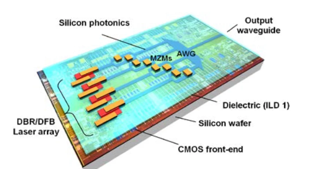
Nguyen also led another Inphi group in developing an in-house silicon photonics design capability.
These two core technologies – silicon photonics and PAM4 – would prove key in Inphi’s fortunes and gain the company a key design win with hyperscaler Microsoft with the COLORZ optical module.
Microsoft met Inphi staff at a show and described wanting a 100Gbps optical module that could operate over 80km to link data centre sites yet would consume under 3.5W. No design had done that before.
Inphi had PAM4 and silicon photonics by then and worked with Microsoft for a year to make it happen. “That’s how innovation happens; give engineers a good problem, and they figure out how to solve it,” says Nguyen.

Marvell transformation
The COVID-19 pandemic created unlikely opportunities. Marvell’s CEO, Matt Murphy, and then-Inphi CEO, Ford Tamer, served on the Semiconductor Industry Association (SIA) board together. It led to them discussing a potential acquisition during hikes in the summer of 2020 when offices were closed. By 2021, Marvell acquired Inphi for $10 billion.
“Matt asked me to stay on to help with the transition,” says Nguyen. “I knew that for the transition to be successful, I could play a key role as an Inphi co-founder.”
Nguyen was promoted to manage most of the Inphi optical portfolio and Marvell’s copper physical layer portfolio.
“Matt runs a much bigger company, and he has very well thought-out measurement processes that he runs throughout the year,” he says. “It is one of those things that I needed to learn: how to do things differently.”
The change as part of Marvell was welcome. “It invigorated me and asked me to take stock of who I am and what skills I bring to the table,” says Nguyen.
AI and connectivity
After helping ensure a successful merger integration, Nguyen returned to his engineering roots, focusing on optical connectivity for AI. By studying how companies like Nvidia, Google, and Amazon architect their networks, he gained insights into future infrastructure needs.
“You can figure out roughly how many layers of switching they will need for this and the ratio between optical interconnect and the GPU, TPU or xPU,” he says. “Those are things that are super useful.”
Nguyen says there are two “buckets” to consider: scale-up and scale-out networks. Scale-out is needed when connecting 10,000s, 100,000 and, in the future, 1 million xPUs via network interface cards. Scale-out networks use protocols such as Infiniband or Ethernet that minimise and handle packet loss.
Scale-up refers to the interconnect between xPUs in a very high bandwidth, low latency network. This more local network allows the xPUs to share each other’s memory. Here, copper is used: it is cheap and reliable. “Everyone loves copper,” says Nguyen. But copper’s limitation is reach, which keeps shrinking as signalling speeds increase.
“At 200 gigabits, if you go outside the rack, optics is needed,” he says. “So next-gen scale-up represents a massive opportunity for optics,” he says.
Nguyen notes that scale-up and scale-out grow in tandem. It was eight xPUs in a scale-up for up to a 25,000 xPU scale-out network cluster. Now, it is 72 xPUs scale-up for a 100,000 xPU cluster. This trend will continue.
Beyond Technology
Nguyen’s passion for wildlife photography is due to his wife. Some 30 years ago, he and his wife supported the reintroduction of wolves to the Yellowstone national Park in the US.
After Inphi’s initial public offering (IPO) in 2010, Nguyen could donate money to defend wildlife, and he and his wife were invited to a VIP retreat there.
“I just fell in love with the place and started taking up photography,” he says. Though initially frustrated by elusive wolves, his characteristic determination took over. “The thing about me is that if I’m into something, I want to be the best at it. I don’t dabble in things,” he says, laughing. “I’m very obsessive about what I want to spend my time on.
He has travelled widely to pursue his passion, taking what have proved to be award-winning photos.
Full Circle: becoming a role model
Perhaps most meaningful in Nguyen’s next chapter is his commitment to Vietnam, where he’s been embraced as a high-tech role model and a national hero.
He plans to encourage young people to pursue engineering careers and develop Vietnam’s high-speed semiconductor industry, completing a circle that began with his departure decades ago.
He also wants to spend time with his wife and family, including going on an African safari.
He won’t miss back-to-back Zoom calls and evenings away from home. In the last two years, he estimates that he has been away from home between 60 and 70 per cent of the time.
It seems retirement isn’t an ending but a new beginning.

DIMENSION tackles silicon photonics’ laser shortfall
Several companies and research institutes, part of a European project, are developing a silicon photonics process that combines on-chip electronics and lasers. Dubbed Dimension (Directly Modulated Lasers on Silicon), the silicon photonics project is part of the European Commission’s Horizon 2020 research and innovation programme.
 The Dimension process showing the passive photonics, dielectric material, BiCMOS circuitry, and the on-chip lasers and modulators. The indium phosphide material is shown in red. Source: Dimension.
Goal
Silicon photonics has long been seen as a technology having the potential to deliver optical devices at CMOS manufacturing costs. But silicon's key shortfall is that it does not lase. “What we see with today’s solutions is a very low-cost chip with a lot of functionality, which is a great thing, but in addition you need lasers,” says Bert Offrein, principal research staff member and manager of neuromorphic devices and systems at IBM Research, a participant in the Dimension project.
The laser accounts for a relatively large fraction of the total bill of materials of a silicon photonics chip. In turn, connecting the light source to the chip is not trivial and adds to the packaging costs. “In this project, we try to tackle this [laser] issue,” says Offrein.
The project's goal is to develop manufacturing processes that will enable the integration of photonics, including the laser, and electronics, all on one chip. “By fully integrating the laser on the chip, we massively reduce the cost and create additional functionality,” says Offrein.
“This is the true embodiment of what people first pictured as silicon photonics: the combination of optics and electronics on a single chip,” says Lars Zimmermann, team leader, silicon photonics at the Innovations for High Performance Microelectronics (IHP) research institute, another member of Dimension.
Proof-of-concept demonstrators
Dimension is a four-year project that will end in early 2020. Other project participants besides IBM Research and the IHP include ADVA Optical Networking, Opticap and the Athens Information Technology (AIT) research centre. The Dresden University of Technology is overseeing the project.
The project has set itself the goal of producing three proof-of-concept designs using the integrated silicon photonics technology.
One is a 400 Gigabit Ethernet (GbE) transmitter made up of eight 50 gigabit-per-second (Gbps) channels, each comprising a 25 gigabaud directly-modulated laser combined with 4-level pulse amplitude modulation (PAM4). Two variants are planned: a directly modulated version for the 400GbE 2km reach specification, and one with external modulation for the 400GbE 10km reach standard.
Another design is a coherent transmitter for such applications as data centre interconnect, compromising a monolithically integrated narrow-linewidth tunable laser, modulator and driver. The coherent transmitter will have a 10km target reach, will operate at 25Gbps and have a tunable narrow linewidth of under 1MHz.
The third, final demonstrator is a directly-modulated 25-gigabit non-return-to-zero laser using indium phosphide grown directly on the silicon.
By fully integrating the laser on the chip, we massively reduce the cost and create additional functionality
Process details
The silicon photonics manufacturing process involves using a silicon-on-insulator (SOI) wafer to implement the passive photonics functions and the electronics. The electronics supports high-speed analogue driver transistors and a 0.25-micron BiCMOS process used to implement the chip's control logic and control interfaces.
 Bert Offrein
The laser is constructed by first bonding a thin layer of indium phosphide. “It is structured in such a way that it [the III-V material] can be embedded completely in the whole CMOS processing,” says Offrein.
The indium phosphide layer, referred to as a III-V membrane, sits on a thin dielectric layer placed on the SOI wafer. The dielectric material is needed to protect the wafer from contamination by the III-V material and ensure that such a design could be manufactured in a BiCMOS foundry.
Once the thin indium phosphide layer is deposited, the laser can be constructed. The final stages, part of the chip-making back-end process, is the adding of metallisation layers that connect the laser and the electronics, and the circuits to the interface signals.
Growing lasers on silicon
Growing the indium phosphide layer directly on silicon, as will be done for the third demonstrator, is more exploratory. “We want to show there is a path forward on this III-V-on-silicon technology to reduce the cost further,” says Offrein.
 Lars Zimmermann
The challenge growing indium phosphide on silicon is the lattice mismatch that occurs between the two materials which leads to defects.
To tackle the issue, an approach known as confined growth is used. A small ‘seed’ is put on the silicon to act as a growth point for the indium phosphide. A small cavity is created using silica to confine the resulting growth. “The material grows in this glass cavity and the defects grow out and disappear at the edges,” says Offrein. “You then have a very high-quality III-V in this glass and this is the starting point to continue to build the quantum wells that we need.”
One challenge is enlarging the confined growth area. So far, such growth is limited to a micron whereas the length of a laser can be 500 microns typically. And once the laser is built, there remain the issues of laser reliability and temperature stability. “We will see challenges but we are not there yet,” says Offrein.
This is the true embodiment of what people first pictured as silicon photonics: the combination of optics and electronics on a single chip
Status
Dimension is tackling designs for communications but such on-chip lasers will also be useful for a range of applications such as optical sensing, says Offrein.
The project is coming to the end of its first year. Its members are creating the basic building blocks needed to realise the lasers on the silicon wafer. IBM has demonstrated the basic functionality by bonding indium phosphide to its own passive silicon photonics technology. “We have also realised the first lasers - not yet electrically pumped but optically pumped,” says Offrein. The performance of these lasers is now being characterised.
All the processes needed to pump the lasers electrically are now in place and the goal is to build complete laser structures by March 2017.
IBM is also working with IHP to see what is required to implement the technology using IHP’s own silicon photonics process. IHP is currently testing IBM’s wafers regarding any contamination issues before testing the integration process.
ADVA Optical Networking would not be on board if they were not expecting eventually to have such technology available for their products
Exploitation
The European Commission has a long history of programmes backing leading-edge research. However, Europe's track record of exploiting such research to achieve market-leading companies and products has been limited.
The European Commission staff involved in planning the Horizon 2020 projects have been far more active in ensuring that these projects are exploited, says Zimmermann. "ADVA Optical Networking would not be on board if they were not expecting eventually to have such technology available for their products," he adds.
If Dimension proves successful, IHP could make available the integrated silicon photonics process to companies to implement their opto-electronic integrated circuit designs.
IBM, while no longer a semiconductor manufacturer, would also be keen for the technology to be transferred to large foundries such as STMicroelectronics and GlobalFoundries. “That way we could purchase the technology and apply it in our own systems,” says Offrein.
Article amended on Nov 29th. Added details about the proof-of-concept demonstrators.
NeoPhotonics showcases a CFP2-ACO roadmap to 400G
The company demonstrated the CFP2-ACO module transmitting at 100 gigabit using polarisation multiplexed, quadrature phase-shift keying (PM-QPSK) modulation at the recent OFC show. The line-side module is capable of transmitting over 1,000km and also supports PM-16QAM that doubles capacity over metro network distances.
 Ferris LipscombThe CFP2-ACO is a Class 3 design: the control electronics for the modulator and laser reside on the board, alongside the coherent DSP-ASIC chip.
At OFC, NeoPhotonics also demonstrated single-wavelength 400-gigabit transmission using more advanced modulation and a higher symbol rate, and a short-reach 100-gigabit link for inside the data centre using 4-level pulse-amplitude modulation (PAM4) signalling.
Roadmap to 400 gigabit
One benefit of the CFP2-ACO is that the pluggable module can be deployed only when needed. Another is that the optics will work with coherent DSP-ASICs for different systems vendors and merchant chip suppliers.
“After a lot of technology-bragging about the CFP2-ACO, this is the year it is commercial,” says Ferris Lipscomb, vice president of marketing at NeoPhotonics.
Also demonstrated were the components needed for a next-generation CFP2-ACO: NeoPhotonics’ narrow line-width tunable laser and its higher-bandwidth integrated coherent receiver. To achieve 400 gigabit, 32-QAM and a 45 gigabaud symbol rate were used.
Traditional 100-gigabit coherent uses a 32-gigabaud symbol rate. That combined with QPSK and the two polarisations results in a total bit rate of 2 polarisations x 2bits/symbol x 32 gigabaud or 128 gigabits: a 100-gigabit payload and the rest overhead bits. Using 32-QAM instead of QPSK increases the number of bits encoded per symbol from 2 to 5, while increasing the baud rate from 32 to 45 gigabaud adds a speed-up factor of 1.4. Combining the two, the resulting bit rate is 45 gigabaud x 5bits/symbol x 2 polarisations or 450 gigabit overall.
After a lot of technology-bragging about the CFP2-ACO, this is the year it is commercial
Using 32-QAM curtails the transmission distance to 100km due to the denser constellation but such distances are suited for data centre interconnect applications.
“That was the demo [at OFC] but the product is also suitable for metro distances of 500km using 16-QAM and long-haul of 1,000km using 200 gigabit and 8-QAM,” says Lipscomb.
PAM4
The PAM4 demonstration highlighted NeoPhotonics’ laser and receiver technology. The company showcased a single-wavelength link running at 112 gigabits-per-second using its 56Gbaud externally modulated laser (EML) with an integrated driver. The PAM4 link can span 2km in a data centre.
“What is not quite ready for building into modules is the [56Gbaud to 112 gigabit PAM4] DSP, which is expected to be out in the middle to the second half of the year,” says Lipscomb. The company will develop its own PAM4-based optical modules while selling its laser to other module makers.
Lipscomb says four lanes at 56 gigabaud using PAM4 will deliver a cheaper 400-gigabit solution than eight lanes, each at 25 gigabaud.
Silicon Photonics
NeoPhotonics revealed that it is supplying new 1310nm and 1550nm distributed feedback (DFB) lasers to optical module players that are using silicon photonics for their 100-gigabit mid-reach transceivers. These include the 500m PSM-4, and the 2km CWDM4 and CLR4.
Lipscomb says the benefits of its lasers for silicon photonics include their relatively high output power - 40 to 60mW - and the fact that the company also makes laser arrays which are useful for certain silicon photonics applications.
NeoPhotonics’ laser products have been for 100-gigabit modules with reaches of 2km to 10km. “Silicon photonics is usually used for shorter reaches of a few hundred meters,” says Lipscomb. “This new product is our first one aimed at the short reach data centre market segment.”
“Our main products have been for 100-gigabit modules for the longer reaches of 2km to 10km,” says Lipscomb. “Silicon photonics is usually used for shorter reaches of a few hundred meters, and this new [laser] product is our first one aimed at the short reach data centre market segment."
The company says it has multiple customer engagements spanning various wavelength plans and approaches for Nx100-gigabit data centre transceiver designs. Mellanox Technologies is one vendor using silicon photonics that NeoPhotonics is supplying.