
Oclaro’s 400-gigabit plans
Adam Carter, Oclaro’s chief commercial officer, discusses the company’s 400-gigabit and higher-speed coherent optical transmission plans and the 400-gigabit client-side pluggable opportunity.
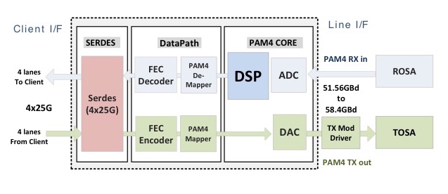
Oclaro showcased its first coherent module that uses Ciena’s WaveLogic Ai digital signal processor at the ECOC show held recently in Gothenburg.
 Adam CarterOclaro is one of three optical module makers, the others being Lumentum and NeoPhotonics, that signed an agreement with Ciena earlier this year to use the system vendor’s DSP technology and know-how to bring coherent modules to market. The first product resulting from the collaboration is a 5x7-inch board-mounted module that supports 400-gigabits on a single-wavelength.
The first WaveLogic Ai-based modules are already being tested at several of Oclaro’s customers’ labs. “They [the module samples] are very preliminary,” says Adam Carter, the chief commercial officer at Oclaro. “The really important timeframe is when we get towards the new year because then we will have beta samples.”
DSP developments
The coherent module is a Ciena design and Carter admits there isn’t going to be much differentiation between the three module makers’ products.
“We have some of the key components that sit inside that module and the idea is, over time, we would design in the rest of the componentry that we make that isn’t already in there,” says Carter. “But it is still going to be the same spec between the three suppliers.”
The collaboration with the module makers helps Ciena promote its coherent DSP to a wider market and in particular China, a market where its systems are not deployed.
Over time, the scope for differentiation between the three module makers will grow. “It [the deal] gives us access to another DSP chip for potential future applications,” says Carter.
Here, Oclaro will be the design authority, procuring the DSP chip for Ciena before adding its own optics. “So, for example, for the [OIF’s] 400G ZR, we would ask Ciena to develop a chip to a certain spec and then put our optical sub-assemblies around it,” says Carter. “This is where we do believe we can differentiate.”
Oclaro also unveiled at ECOC an integrated coherent transmitter and an intradyne coherent receiver optical sub-assemblies using its indium phosphide technology that operate at up to 64 gigabaud (Gbaud).
We expect to see 64Gbaud optical systems being trialed in 2018 with production systems following at the end of next year
A 64Gbaud symbol rate enables a 400-gigabit wavelength using 16-ary quadrature amplitude modulation (16-QAM) and a 600-gigabit wavelength using 64-QAM.
Certain customers want such optical sub-assemblies for their line card designs and Oclaro will also use the building blocks for its own modules. The devices will be available this quarter. “We expect to see 64Gbaud optical systems being trialed in 2018 with production systems following at the end of next year and the beginning of 2019,” says Carter.
Oclaro also announced that its lithium niobate modulator supporting 400-gigabit single wavelengths is now in volume production. “Certain customers do have their preferences when it comes to first designs and particularly for long-reach systems,” says Carter. “Lithium niobate seems to be the one people go with.”
400-gigabit form factors
Oclaro did not make any announcements regarding 400-gigabit client-side modules at ECOC. At the OFC show held earlier this year, it detailed two CFP8-based 400-gigabit designs based on eight wavelengths with reaches of 10km and 40km.
“We are sampling the 400-gigabit 10km product right now,” says Carter. “The product is being tested at the system level and will go through various qualification runs.”
The 40km CFP8 product is further out. There are customers interested in such a module as they have requirements to link IP routers that are more than 10km apart.
Carter describes the CFP8 400-gigabit modules as first-generation products. The CFP8 is similar in size to the CFP2 pluggable module and that is too large for the large-scale data centre players. They want higher aggregate bandwidth and greater front panel densities for their switches and are looking such form factors as the double-density QSFP (QSFP-DD) and the Octal Small Form Factor pluggable (OSFP).
The OSFP is a fresh design, has a larger power envelope - some 15W compared to the 12W of the QSFP-DD - and has a roadmap that supports 800-gigabit data rates. In contrast, the QSFP-DD is backward compatible with the QSFP, an attractive feature for many vendors.
But it is not only a module’s power envelope that is an issue for 400-gigabit designs but also whether a one-rack-unit box can be sufficiently cooled when fully populated to avoid thermal runaway. Some 36 QSFP-DDs can fit on the front panel compared to 32 OSFPs.
Carter stresses both form factors can’t be dismissed for 400-gigabit: “Everyone is pursuing designs that are suitable for both.” Oclaro is not an advocate of either form factor given it provides optical sub-assemblies suitable for both.
The industry really wants four-channels. When you use more lasers, you are adding more cost.
Optical formats
Oclaro’s core technology is indium phosphide and, as such, its focusses on single-mode fibre designs.
The single mode options for 400 gigabits are split between eight-wavelength designs such as the IEEE 802.3bs 2km 400GBASE-FR8 and 10km 400GBASE-LR8 and the newly announced CWDM8 MSA, and four-wavelength specifications - the 500m IEEE 802.3bs parallel fibre 400GBASE-DR4 and the 2km 100G Lambda MSA 400G-FR4 that is under development. Oclaro is a founding member of the 100 Gigabit Lambda MSA but has not joined the CWDM8 MSA.
"The industry really wants four channels," says Carter. "When you use more lasers, you are adding more cost." It is also not trivial fitting eight lasers into a CFP8 never mind into the smaller QSFP-DD and OSFP modules.
“There might be some that have the technology to do the eight-channel part and there might be customers that will use that,” says Carter. “But most of the discussions we’ve been having are around four channels.”
Challenges
The industry’s goal is to have 400-gigabit QSFP-DD and OSFP module in production by the end of next year and into 2019. “There is still some risk but everybody is driving to meet that schedule,” says Carter.
Oclaro says first samples of 100-gigabit PAM-4 chips needed for 100-gigabit single wavelengths are now in the labs. Module makers can thus add their optical sub-assemblies to the chips and start testing system performance. Four-channel PAM-4 chips will be needed for the 400-gigabit module products.
Carter also acknowledges that any further delay in four-wavelength designs could open the door for other 400-gigabit solutions and even interim 200-gigabit designs.
“As a transceiver supplier and an optical component supplier you are always aware of that,” he says. “You have to have backup plans if that comes off.”
The CWDM8 MSA avoids PAM-4 to fast-track 400G
Another multi-source agreement (MSA) group has been created to speed up the market introduction of 400-gigabit client-side optical interfaces.
The CWDM8 MSA is described by its founding members as a pragmatic approach to provide 400-gigabit modules in time for the emergence of next-generation switches next year. The CWDM8 MSA was announced at the ECOC show held in Gothenburg last week.
 Robert BlumThe eight-wavelength coarse wavelength-division multiplexing (CWDM) MSA is being promoted as a low-cost alternative to the IEEE 803.3bs 400 Gigabit Ethernet Task Force’s 400-gigabit eight-wavelength specifications, and less risky than the newly launched 100G Lambda MSA specifications based on four 100-gigabit wavelengths for 400 gigabit.
“The 100G Lambda has merits and we are also part of that MSA,” says Robert Blum, director of strategic marketing and business development at Intel’s silicon photonics product division. “We just feel the time to get to 100-gigabit-per-lambda is really when you get to 800 Gigabit Ethernet.”
Intel is one of the 11 founding companies of the CWDM8 MSA.
Specification
The CWDM8 MSA will develop specifications for 2km and 10km links. The MSA uses wavelengths spaced 20nm apart. As a result, unlike the IEEE’s 400GBASE-FR8 and 400GBASE-LR8 that use the tightly-spaced LAN-WDM wavelength scheme, no temperature control of the lasers is required. “It is just like the CWDM4 but you add four more wavelengths,” says Blum.
The CWDM8 MSA also differs from the IEEE specifications and the 100G Lambda MSA in that it does not use 4-level pulse-amplitude modulation (PAM-4). Instead, 50-gigabit non-return-to-zero (NRZ) signalling is used for each of the eight wavelengths.
The MSA will use the standard CDAUI-8 8x50-gigabit PAM-4 electrical interface. Accordingly, a retimer chip will be required inside the module to translate the input 50-gigabit PAM electrical signal to 50-gigabit NRZ. According to Intel, several companies are developing such a chip.
When we looked at what is available and how to do an optical interface, there was no good solution that would allow us to meet those timelines
Benefits
Customers are telling Intel that they need 400-gigabit duplex-fibre optical modules early next year and that they want to have them in production by the end of 2018.
“When we looked at what is available and how to do an optical interface, there was no good solution that would allow us to meet those timelines, fit the power budget of the QSFP-DD [module] and be at the cost points required for data centre deployment,” says Blum.
An 8x50-gigabit NRZ approach is seen as a pragmatic solution to meet these requirements.
No PAM-4 physical layer DSP chip is needed since NRZ is used. The link budget is significantly better compared to using PAM-4 modulation. And there is a time-to-market advantage since the technologies used for the CWDM8 are already proven.
We just think it [100-gigabit PAM4] is going to take longer than some people believe
This is not the case for the emerging 100-gigabit-per-wavelength MSA that uses 50-gigabaud PAM-4. “PAM-4 makes a lot of sense on the electrical side, a low-bandwidth [25 gigabaud], high signal-to-noise ratio link, but it is not the ideal when you have high bandwidth on the optical components [50 gigabaud] and you have a lot of noise,” says Blum.
One-hundred-gigabit-per-wavelength will be needed for the optical path, says Blum, but for 800 Gigabit Ethernet with its eight electrical channels and eight optical ones. “We just think it [100-gigabit PAM4] is going to take longer than some people believe.” Meanwhile, the CWDM8 is the best approach to meet market demand for a 400-gigabit duplex interfaces to support next-generation data centre switches expected next year, says Blum.
The founding members of the CWDM8 MSA include chip and optical component players as well as switch system makers. Unlike the 100G Lambda MSA, no larger-scale data centre operators have joined the MSA.
The members are Accton, Barefoot Networks, Credo Semiconductor, Hisense, Innovium, Intel, MACOM, Mellanox, Neophotonics and Rockley Photonics.
MultiPhy unveils 100G single-wavelength PAM-4 chip
A chip to enable 100-gigabit single-wavelength client-side optical modules has been unveiled by MultiPhy. The 100-gigabit 4-level pulse amplitude modulation (PAM-4) circuit will also be a key building block for 400 Gigabit Ethernet interfaces that use four wavelengths.
 Source: MultiPhy
Dubbed the MPF3101, the 100-gigabit physical layer (PHY) chip is aimed at such applications as connecting switches within data centres and for 5G cloud radio access network (CRAN).
“The chip has already been sent out to customers and we are heading towards market introductions,” says Avi Shabtai, CEO of MultiPhy.
The MPF3101 will support 100-gigabit over 500m, 2km and 10km.
The IEEE has developed the 100-gigabit 100GBASE-DR standard for 500m while the newly formed 100G Lambda MSA (multi-source agreement) is developing specifications for the 2km 100-gigabit single-channel 100G-FR and the 10km 100G-LR.
MultiPhy says the QSFP28 will be the first pluggable module to implement a 100-gigabit single-wavelength design using its chip. The SFP-DD MSA, currently under development, will be another pluggable form factor for the single-wavelength 100-gigabit designs.
The chip has already been sent out to customers and we are heading towards market introductions
400 Gigabit
The 100-gigabit IP will also be a key building block for a second MultiPhy chip for 400-gigabit optical modules needed for next-generation data centre switches that have 6.4 and 12.8 terabits of capacity. “This is the core engine for all these markets,” says Shabtai.
Companies have differing views as to how best to address the 400-gigabit interconnect market. There is a choice of form factors such as the OSFP, QSFP-DD and embedded optics based on the COBO specification, as well as emerging standards and MSAs.
The dilemma facing companies is what approach will deliver 400-gigabit modules to coincide with the emergence of next-generation data centre switches.
One consideration is the technical risk associated with implementing a particular design. Another is cost, with the assumption that 4-wavelength 400-gigabit designs will be cheaper than 8x50-gigabit based modules but that they may take longer to come to market.
For 400 gigabits, the IEEE 803.3bs 400 Gigabit Ethernet Task Force has specified the 400GBASE-DR4, a 500m-reach four-wavelength specification that uses four parallel single-mode fibres. The 100G Lambda MSA is also working on a 400-gigabit 2km specification based on coarse wavelength-division multiplexing (CWDM), known as 400G-FR4, with work on a 10km reach specification to start in 2018.
We are hearing a lot in the industry about 50-gigabit-per-lambda. For us, this is old news; we are moving to 100-gigabit-per-lambda and we believe the industry will align with us.
And at ECOC 2017 show, held last week in Gothenburg, another initiative - the CWDM8 MSA - was announced. The CWDM8 is an alternative design to the IEEE specifications that sends eight 50-gigabit non-return-to-zero signals rather that PAM-4 over a fibre.
“We are hearing a lot in the industry about 50-gigabit-per-lambda,” says Shabtai. “For us, this is old news; we are moving to 100-gigabit-per-lambda and we believe the industry will align with us.”
Chip architecture
The MPF3101, implemented using a 16nm CMOS process, supports PAM-4 at symbol rates up to 58 gigabaud.
The chip’s electrical input is four 25-gigabit lanes that are multiplexed and encoded into a 50-plus gigabaud PAM-4 signal that is fed to a modulator driver, part of a 100-gigabit single-channel transmitter optical sub-assembly (TOSA). A 100-gigabit receiver optical sub-assembly (ROSA) feeds the received PAM-4 encoded signal to the chip’s DSP before converting the 100-gigabit signal to 4x25 gigabit electrical signals (see diagram).
“If you need now only one laser and one optical path [for 100 gigabits] instead of four [25 gigabits optical paths], that creates a significant cost reduction,” says Shabtai.
The advent of a single-wavelength 100-gigabit module promises several advantages to the industry. One is lower cost. Estimates that MultiPhy is hearing is that a single-wavelength 100-gigabit module will be half the cost of existing 4x25-gigabit optical modules. Such modules will also enable higher-capacity switches as well as 100-gigabit breakout channels when connected to a 400-gigabit four-wavelength module. Lastly, MultiPhy expects the overall power consumption to be less.
Availability
MultiPhy says first 100-gigabit single-wavelength QSFP28s will appear sometime in 2018.
The company is being coy as to when it will have a 400-gigabit PAM-4 chip but it points out that by having working MPF3101 silicon, it is now an integration issue to deliver a 4-channel 400-gigabit design.
As for the overall market, new high-capacity switches using 400-gigabit modules will start to appear next year. The sooner four-channel 400-gigabit PAM-4 silicon and optical modules appear, the less opportunity there will be for eight-wavelength 400-gigabit designs to gain a market foothold.
“That is the race we are in,” says Shabtai.
Inphi unveils a second 400G PAM-4 IC family
Inphi has announced the Vega family of 4-level, pulse-amplitude modulation (PAM-4) chips for 400-gigabit interfaces.
 The 16nm CMOS Vega IC family is designed for enterprise line cards and is Inphi’s second family of 400-gigabit chips that support eight lanes of 50-gigabit PAM-4.
Its first 8x50-gigabit family, dubbed Polaris, is used within 400-gigabit optical modules and was announced at the OFC show held in Los Angeles in March.
“Polaris is a stripped-down low-power DSP targeted at optical module applications,” says Siddharth Sheth, senior vice president, networking interconnect at Inphi (pictured). “Vega, also eight by 50-gigabits, is aimed at enterprise OEMs for their line-card retimer and gearbox applications.”
A third Inphi 400-gigabit chip family, supporting four channels of 100-gigabit PAM-4 within optical modules, will be announced later this year or early next year.
400G PAM-4 drivers
Inphi’s PAM-4 chips have been developed in anticipation of the emergence of next-generation 6.4-terabit and 12.8-terabit switch silicon and accompanying 400-gigabit optical modules such as the OSFP and QSFP-DD form factors.
Sheth highlights Broadcom’s Tomahawk-III, start-up Innovium’s Teralynx and Mellanox’s Spectrum-2 switch silicon. All have 50-gigabit PAM-4 interfaces implemented using 25-gigabaud signalling and PAM-4 modulation.
“What is required is that such switch silicon is available and mature in order for us to deploy our PAM-4 products,” says Sheth. “Everything we are seeing suggests that the switch silicon will be available by the end of this year and will probably go into production by the end of next year,” says Sheth.
Several optical module makers are starting to build 8x50-gigabit OSFP and QSFP-DD products
The other key product that needs to be available is the 400-gigabit optical modules. The industry is pursuing two main form factors: the OSFP and the QSFP-DD. Google and switch maker Arista Networks are proponents of the OSFP form factor while the likes of Amazon, Facebook and Cisco back the QSFP-DD. Google has said that it will initially use an 8x50-gigabit module implementation for 400 gigabit. Such a solution uses existing, mature 25-gigabit optics and will be available sooner than the more demanding 4x100-gigabit design that Amazon, Facebook and Cisco are waiting for. The 4x100 gigabit design requires 50Gbaud optics and a 50Gbaud PAM-4 chip.
Inphi says several optical module makers are starting to build 8x50-gigabit OSFP and QSFP-DD products and that its Polaris and Vega family of chips anticipate such deployments.
“We expect 100-gigabit optics to be available sometime around mid-2018 and our next-generation 100-gigabit PAM-4 will be available in the early part of next year,” says Sheth.
Accordingly, the combination of the switch silicon and optics means that the complete ecosystem will already exist next year, he says
Vega
The Polaris chip, used within an optical module, equalises the optical non-linearities of the incoming 50-gigabit PAM-4 signals. The optical signal is created using 25-gigabit lasers that are modulated using a PAM-4 signal that encodes two bits per signal. “When you run PAM-4 over fibre - whether multi-mode or single mode - the signal undergoes a lot of distortion,” says Sheth. “You need the DSP to clean up that distortion.”
The Vega chip, in contrast, sits on enterprise line cards and adds digital functionality that is not supported by the switch silicon. Most enterprise boxes support legacy data rates such as 10 gigabit and 1 gigabit. The Vega chip supports such legacy rates as well as 25, 50, 100, 200 and 400 gigabit, says Sheth.
The Vega chip can add forward-error correction to a data stream and decode it. As well as FEC, the chip also has physical coding sublayer (PCS) functionality. “Every time you need to encode a signal with FEC or decode it, you need to unravel the Ethernet data stream and then reassemble it,” says Sheth.
Also on-chip is a crossbar that can switch any lane to any other lane before feeding the data to the switch silicon.
Sheth stresses that not all switch chip applications need the Vega. For large-scale data centre applications that use stripped-down systems, the optical module would feed the PAM-4 signal directly into the switch silicon, requiring the use of the Polaris chip only.
A second role for Vega is driving PAM-4 signals across a system. “If you want to drive 50-gigabit PAM-4 signals electrically across a system line card and noisy backplane then you need a chip like Vega,” says Sheth.
A further application for the Vega chip is as a ‘gearbox’, converting between 50-gigabit and 25-gigabit line rates. Once high-capacity switch silicon with 50G PAM-4 signals are deployed, the Vega chip will enable the conversion between 50-gigabit PAM-4 and 25-gigabit non-return-to-zero (NRZ) signals.System vendors will then be able to interface 100-gigabit (4x25-gigabit) QSFP28 modules with these new switch chips.
One hundred gigabit modules will be deployed for at least another three to four years while the price of such modules has come down significantly. “For a lot of the cloud players it comes down to cost: are 128-ports at 100-gigabit cheaper that 32, 400-gigabit modules?” says Sheth. The company says it is seeing a lot of interest in this application.
We expect 100-gigabit optics to be available sometime around mid-2018 and our next-generation 100-gigabit PAM-4 will be available in the early part of next year
Availability
Inphi has announced two Vega chips: a 400-gigabit gearbox and a 400-gigabit retimer and gearbox IC. “We are sampling,” says Sheth. “We have got customers running traffic on their line cards.” General availability is expected in the first quarter of 2018.
As for the 4x100-gigabit PAM-4 chips, Sheth expects solutions to appear in the first half of next year: “We have to see how mature the optics are at that point and whether something can go into production in 2018.”
Inphi maintains that the 8x50-gigabit optical module solutions will go to market first and that the 4x100-gigabit variants will appear a year later. “If you look at our schedules, Polaris and the 4x100-gigabit PAM-4 chip are one year apart,” he says.
SFP-DD: Turning the SFP into a 100-gigabit module
An industry initiative has started to quadruple the data rate of the SFP, the smallest of the pluggable optical modules. The Small Form Factor Pluggable – Double Density (SFP-DD) is being designed to support 100 gigabits by doubling the SFP’s electrical lanes from one to two and doubling their speed.
 Scott SommersThe new multi-source agreement (MSA), to be completed during 2018, will be rated at 3.5W; the same power envelope as the current 100-gigabit QSFP module, even though the SFP-DD is expected to be 2.5x smaller in size.
The front panel of a 1-rack-unit box will be able to support up to 96 SFP-DD modules, a total capacity of 9.6 terabits.
The SFP-DD is adopting a similar philosophy as that being used for the 400-gigabit QSFP-DD MSA: an SFP-DD port will support legacy SFPs modules - the 25-gigabit SFP28 and 10-gigabit SFP - just as the QSFP-DD will be backward compatible with existing QSFP modules.
“Time and time again we have heard with the QSFP-DD that plugging in legacy modules is a key benefit of that technology,” says Scott Sommers, group product manager at Molex and the chair of the new SFP-DD MSA. Sommers is also a co-chair of the QSFP-DD MSA.
Interest in the SFP-DD started among several like-minded companies at the OFC show held in March. Companies such as Alibaba, Molex, Hewlett Packard Enterprise and Huawei agreed on the need to extend the speed and density of the SFP similar to how the QSFP-DD is extending the QSFP.
The main interest in the SFP-DD is for server to top-of-rack switch connections. The SFP-DD will support one or two lanes of 28 gigabit-per-second (Gbps) or of 56Gbps using 4-level pulse-amplitude modulation (PAM-4).
“We tried to find server companies and companies that could help with the mechanical form factor like connector companies, transceiver companies and systems companies,” says Sommers. Fourteen promoter companies supported the MSA at its launch in July.
Specification work
The SFP-DD MSA is developing a preliminary hardware release that will be published in the coming months. This will include the single-port surface mount connector, the cage surrounding it and the module’s dimensions.
The goal is that the module will be able to support 3.5W. “Once we pin down the form factor, we will be able to have a better idea whether 3.5W is achievable,” says Sommers. “But we are very confident with the goal.”
The publication of the mechanical hardware specification will lead to other companies - contributors - responding with their comments and suggestions. “This will make the specification better but it does slow down things,” says Sommers.
The MSA’s attention will turn to the module’s software management specification once the hardware release is published. The software must understand what type of SFP module is plugged into the SFP-DD port, for example.
Supporting two 56Gbps lanes using PAM-4 means that up to four SFP-DD modules can be interfaced to a 400-gigabit QSFP-DD. But the QSFP-DD is not the only 400-gigabit module the SFP-DD could be used with in such a ‘breakout’ mode.“I don’t want to discount the OSFP [MSA],” says Sommers. “That is a similar type of technology to the QSFP-DD where it is an 8-channel-enabling form factor.”
The SFP could eventually support a 200-gigabit capacity. “It is no secret that this industry is looking to double speeds every few years,” says Sommers. He stresses this isn't the goal at present but it is there: “This MSA, for now, is really focussed on 25-gigabit non-return-to-zero or 50-gigabit PAM-4.”
Challenges
One challenge Sommers highlights for the SFP-DD is achieving a mechanically robust design: achieving the 3.5W as well as the signal integrity given the two lanes of 56Gbps.
The signal integrity advances achieved with the QSFP-DD work will be adopted for the SFP-DD. “That is why we don’t think it is going to take as long as the QSFP-DD,” he says.
The electro-optic components need to be squeezed into a smaller space and with the SFP-DD’s two lanes, there is a doubling of the copper lines going into the same opening. “This is not insurmountable but it is challenging,” says Sommers.
Further reading
Mellanox blog on the SFP-DD, click here
Ranovus shows 200 gigabit direct detection at ECOC
Ranovus has announced it first direct-detection optical products for applications including data centre interconnect.
 Saeid AramidehThe start-up has announced two products to coincide with this week’s ECOC show being held in Dusseldorf, Germany.
One product is a 200 gigabit-per-second (Gbps) dense wavelength-division multiplexing (WDM) CFP2 pluggable optical module that spans distances up to 130km. Ranovus will also sell the 200Gbps transmitter and receiver optical engines that can be integrated by vendors onto a host line card.
The dense WDM direct-detection solution from Ranovus is being positioned as a cheaper, lower-power alternative to coherent optics used for high-capacity metro and long-haul optical transport. Using such technology, service providers can link their data centre buildings distributed across a metro area.
The cost [of the CFP2 direct detection] proves in much better than coherent
“The power consumption [of the direct-detection design] is well within the envelope of what the CFP2 power budget is,” says Saeid Aramideh, a Ranovus co-founder and chief marketing. The CFP2 module's power envelop is rated at 12W and while there are pluggable CFP2-ACO modules now available, a coherent DSP-ASIC is required to work alongside the module.
“The cost [of the CFP2 direct detection] proves in much better than coherent does,” says Aramideh, although he points out that for distances greater than 120km, the economics change.
The 200Gbps CFP2 module uses four wavelengths, each at 50Gbps. Ranovus is using 25Gbps optics with 4-level pulse-amplitude modulation (PAM-4) technology provided by fabless chip company Broadcom to achieve the 50Gbps channels. Up to 96, 50 Gbps channels can be fitted in the C-band to achieve a total transmission bandwidth of 4.8 terabits.
Ranovus is demonstrating at ECOC eight wavelengths being sent over 100km of fibre. The link uses a standard erbium-doped fibre amplifier and the forward-error correction scheme built into PAM-4.
Technologies
Ranovus has developed several key technologies for its proprietary optical interconnect products. These include a multi-wavelength quantum dot laser, a silicon photonics based ring-resonator modulator, an optical receiver, and the associated driver and receiver electronics.
The quantum dot technology implements what is known as a comb laser, producing multiple laser outputs at wavelengths and grid spacings that are defined during fabrication. For the CFP2, the laser produces four wavelengths spaced 50GHz apart.
For the 200Gbps optical engine transmitter, the laser outputs are fed to four silicon photonics ring-resonator modulators to produce the four output wavelengths, while at the receiver there is an equivalent bank of tuned ring resonators that delivers the wavelengths to the photo-detectors. Ranovus has developed several receiver designs, with the lower channel count version being silicon photonics based.
The quantum dot technology implements what is known as a comb laser, producing multiple laser outputs at wavelengths and grid spacings that are defined during fabrication.
The use of ring resonators - effectively filters - at the receiver means that no multiplexer or demultiplexer is needed within the optical module.
“At some point before you go to the fibre, there is a multiplexer because you are multiplexing up to 96 channels in the C-band,” says Aramideh. “But that multiplexer is not needed inside the module.”
Company plans
The startup has raised $35 million in investment funding to date. Aramideh says the start-up is not seeking a further funding round but he does not rule it out.
The most recent funding round, for $24 million, was in 2014. At the time the company was planning to release its first product - a QSFP28 100-Gigabit OpenOptics module - in 2015. Ranovus along with Mellanox Technologies are co-founders of the dense WDM OpenOptics multi-source agreement that supports client side interface speeds at 100Gbps, 400Gbps and terabit speeds.
However, the company realised that 100-gigabit links within the data centre were being served by the coarse WDM CWDM4 and CLR4 module standards, and it chose instead to focus on the data centre interconnect market using its direct detection technology.
Ranovus has also been working with ADVA Optical Networking with it data centre interconnect technology. Last year, ADVA Optical Networking announced its FSP 3000 CloudConnect data centre interconnect platform that can span both the C- and L-bands.
Also planned by Ranovus is a 400-gigabit CFP8 module - which could be a four or eight channel design - for the data centre interconnect market.
Meanwhile, the CFP2 direct-detection module and the optical engine will be generally available from December.
Intel's 100-gigabit silicon photonics move
Intel has unveiled two 100-gigabit optical modules for the data centre made using silicon photonics technology.
 Alexis Bjorlin
The PSM4 and CWDM4/CLR4 100-gigabit modules mark the first commercial application of a hybrid integration technique for silicon photonics, dubbed heterogeneous integration, that Intel has been developing for years.
Intel's 100-gigabit module announcement follows the news that Juniper Networks has entered into an agreement to acquire start-up, Aurrion, for $165 million. Aurrion is another silicon photonics player developing this hybrid integration technology for its products.
Hybrid integration
With heterogeneous integration, materials such as indium phosphide and gallium arsenide can be bonded to the silicon substrate before the 300mm wafer is processed to produce the optical circuit. Not only can lasers be added to silicon but other active devices such as modulators and photo-detectors as well as passive functions such as isolators and circulators.
There is no alignment needed; we align the laser with lithography
Intel is using the technique to integrate the laser as part of the 100-gigabit transceiver designs.
"Once we apply the light-emitting material down to the silicon base wafer, we define the laser in silicon," says Alexis Bjorlin, vice president and general manager, Intel Connectivity Group. “There is no alignment needed; we align the laser with lithography.”
Intel claims it gets the highest coupling efficiency between the laser and the optical waveguide and modulator because it is lithographically defined and requires no further alignment.
100-gigabit modules
Intel is already delivering the 100-gigabit PSM4 module. “First volume shipments are happening now,” says Bjorlin. Microsoft is one Internet content provider that is using Intel’s PSM4.
The chip company is also sampling a 100-gigabit CWDM4 module that also meets the more demanding CLR4 Alliance’s optical specification. The 100-gigabit CLR4 module can be used without forward-error correction hardware and is favoured for applications where latency is an issue such as high-performance computing.
Intel is not the first vendor to offer PSM4 modules, nor is it the first to use silicon photonics for such modules. Luxtera and Lumentum are shipping silicon photonics-based PSM4 modules, while STMicroelectronics is already supplying its PSM4 optical engine chip.
We are right on the cusp of the real 100-gigabit connectivity deployments
“Other vendors have been shipping PSM4 modules for years, including large quantities at 40 gigabit,” says Dale Murray, principal analyst at LightCounting Market Research. “Luxtera has the clear lead in silicon photonics-based PSM4 modules but a number of others are shipping them based on conventional optics.”
The PSM4 is implemented using four independent 25-gigabit channels sent over a single-mode ribbon fibre. Four fibres are used for transmission and four fibres for receive.
“The PSM4 configuration is an interesting design that allows one laser to be shared among four separate output fibres,” says Murray. “As Luxtera has shown, it is an effective and efficient way to make use of silicon photonics technology.”
The CWDM4 is also a 4x25-gigabit design but uses wavelength-division multiplexing and hence a single-mode fibre pair. The CWDM4 is a more complex design in that an optical multiplexer and demultiplexer are required and the four lasers operate at different wavelengths.
“While the PSM4 module does not break new ground, Intel’s implementation of WDM via silicon photonics in a CWDM4/CLR4 module could be more interesting in a low-cost QSFP28 module,” says Murray. WDM-based QSFP28 modules are shipping from a number of suppliers that are using conventional optics, he says.
Intel is yet to detail when it will start shipping the CWDM4/CLR4 module.
Market demand
Bjorlin says the PSM4 and the CWDM4/CLR4 will play a role in the data centre. There are applications where being able to break out 100-gigabit into 25-gigabit signals as offered by the PSM4 is useful, while other data centre operators prefer a duplex design due to the efficient use of fibre.
“We are right on the cusp of the real 100-gigabit connectivity deployments,” she says.
As for demand, Bjorlin expects equal demand for the two module types in the early phases: “Longer term, we will probably see more demand for the duplex solution”.
LightCounting says that 100-gigabit PSM4 modules took an early lead in the rollout of 100 Gigabit Ethernet, with VCSEL-based modules not far behind.
“Some are shipping CWDM4/CLR4 and we expect that market to ramp,” says Murray. “Microsoft and Amazon Web Services seem to like PSM4 modules while others want to stick with modules that can use duplex fibre.
 Source: Intel
Data centre switching
“One of the most compelling reasons to drive silicon photonics in the future is that it is an integratable platform,” says Bjorlin.
Switch silicon from the likes of Broadcom support 3.2 terabits of capacity but this will increase to 6.4 terabits by next year and 12.8 terabits using 4-level pulse amplitude modulation (PAM-4) signalling by 2018 (see chart). And by 2020, 25.6-terabit capacity switch chips are expected.
The demand for 100 gigabit is for pluggable modules that fit into the front panels of data center switches. But the market is evolving to 400-gigabit embedded optics that sit on the line card, she says, to enable these emerging higher-capacity switches. Intel is a member of the Consortium of On-Board Optics (COBO) initiative that is being led by Microsoft.
“When you get to 25.6-terabit switches, you start to have a real problem getting the electrical signals in and out of the switch chip,” says Bjorlin. This is where silicon photonics can play a role in the future by co-packaging the optics alongside the switch silicon.
“There will be a need for an integrated solution that affords the best power consumption, the best bandwidth-density that we can get and effectively position silicon photonics for optical I/O [input/output],” says Bjorlin. “Ultimately, that co-packaging is inevitable.”
FPGAs with 56-gigabit transceivers set for 2017
The company demonstrated a 56-gigabit transceiver using 4-level pulse-amplitude modulation (PAM-4) at the recent OFC show. The 56-gigabit transceiver, also referred to as a serialiser-deserialiser (serdes), was shown successfully working over backplane specified for 25-gigabit signalling only.
 Gilles GarciaXilinx's 56-gigabit serdes is implemented using a 16nm CMOS process node but the first FPGAs featuring the design will be made using a 7nm process. Gilles Garcia says the choice of 7nm CMOS is solely a business decision and not a technical one.
”Optical module [makers] will take another year to make something decent using PAM-4," says Garcia, Xilinx's director marketing and business development, wired communications. "Our 7nm FPGAs will follow very soon afterwards.”
The company is still to detail its next-generation FPGA family but says that it will include an FPGA capable of supporting 1.6 terabit of Optical Transport Network (OTN) using 56-gigabit serdes only. At first glance that implies at least 28 PAM-4 transceivers on a chip but OTN is a complex design that is logic not I/O limited suggesting that the FPGA will feature more than 28, 56-gigabit serdes.
Applications
Xilinx’s Virtex UltraScale and its latest UltraScale+ FPGA families feature 16-gigabit and 25-gigabit transceivers. Managing power consumption and maximising reach of the high-speed serdes are key challenges for its design engineers. Xilinx says it has 150 engineers for serdes design.
“Power is always a key challenge because as soon as you talk about 400-gigabit to 1-terabit per line card, you need to be cautious about the power your serdes will use,” says Garcia. He says the serdes need to adapt to the quality of the traces for backplane applications. Customers want serdes that will support 25 gigabit on existing 10-gigabit backplane equipment.
Xilinx describes its Virtex UltraScale as a 400-gigabit capable single-chip system supporting up to 104 serdes: 52 at 16 gigabit and 52 at 25 gigabit.
The UltraScale+ is rated as a 500-gigabit to 600-gigabit capable system, depending on the application. For example, the FPGA could support three, 200-gigabit OTN wavelengths, says Garcia.
Xilinx says the UltraScale+ reduces power consumption by 35% to 50% compared to the same designs implemented on the UltrasScale. The Virtex UltraScale+ devices also feature dedicated hardware to implement RS-FEC, freeing up programmable logic for other uses. RS-FEC is used with multi-mode fibre or copper interconnects for error correction, says Xilinx. Six UltraScale+ FPGAs are available and the VU13P, not yet out, will feature up to 128 serdes, each capable of up to 32 gigabit.
We don’t need retimers so customers can connect directly to the backplane at 25 gigabit, thereby saving space, power and cost
The UltraScale and UltraScale+ FPGAs are being used in several telecom and datacom applications.
For telecom, 500-gigabit and 1-terabit OTN designs are an important market for the UltraScale FPGAs. Another use for the FPGA serdes is for backplane applications. “We don’t need retimers so customers can connect directly to the backplane at 25 gigabit, thereby saving space, power and cost,” says Garcia. Such backplane uses include OTN platforms and data centre interconnect systems.
The FPGA family’s 16-gigabit serdes are also being used in 10-gigabit PON and NG-PON2 systems. “When you have an 8-port or 16-port system, you need to have a dense serdes capability to drive the [PON optical line terminal’s] uplink,” says Garcia.
For data centre applications, the FPGAs are being employed in disaggregated storage systems that involved pooled storage devices. The result is many 16-gigabit and 25-gigabit streams accessing the storage while the links to the data centre and its servers are served using 100-gigabit links. The FPGA serdes are used to translate between the two domains (see diagram).
 Source: Xilinx
For its next-generation 7nm FPGAs with 56-gigabit transceivers, Xilinx is already seeing demand for several applications.
Data centre uses include server-to-top-of-rack links as the large Internet providers look move from 25 gigabit to 50- and 100-gigabit links. Another application is to connect adjacent buildings that make up a mega data centre which can involve hundreds of 100-gigabit links. A third application is meeting the growing demands of disaggregated storage.
For telecom, the interest is being able to connect directly to new optical modules over 50-gigabit lanes, without the need for gearbox ICs.
Optical FPGAs
Altera, now part of Intel, developed an optical FPGA demonstrator that used co-packaged VCSELs for off-chip optical links. Since then Altera announced its Stratix 10 FPGAs that include connectivity tiles - transceiver logic co-packaged and linked with the FPGA using interposer technology.
Xilinx says it has studied the issue of optical I/O and that there is no technical reason why it can’t be done. But the issue is a business one when integrating optics in an FPGA, he says: “Who is responsible for the yield? For the support?”
Garcia admits Xilinx could develop its own I/O designs using silicon photonics and then it would be responsible for the logic and the optics. “But this is not where we are seeing the business growing,” he says.
Tackling system design on a data centre scale
Interview 1: Andrew Rickman
Silicon photonics has been a recurring theme in the career of Andrew Rickman. First, as a researcher looking at the feasibility of silicon-based optical waveguides, then as founder of Bookham Technologies, and after that as a board member of silicon photonics start-up, Kotura.
 Andrew Rickman
Now as CEO of start-up Rockley Photonics, his company is using silicon photonics alongside its custom ASIC and software to tackle a core problem in the data centre: how to connect more and more servers in a cost effective and scaleable way.
Origins
As a child, Rickman attended the Royal Institution Christmas Lectures given by Eric Laithwaite, a popular scientist who was also a professor of electrical engineering at Imperial College. As an undergraduate at Imperial, Rickman was reacquainted with Professor Laithwaite who kindled his interest in gyroscopes.
“I stumbled across a device called a fibre-optic gyroscope,” says Rickman. “Within that I could see people starting to use lithium niobate photonic circuits.” It was investigating the gyroscope design and how clever it was that made Rickman wonder whether the optical circuits of such a device could be made using silicon rather than exotic materials like lithium niobate.
“That is where the idea triggered, to look at the possibility of being able to make optical circuits in silicon,” he says.
If you try and force a photon into a space shorter than its wavelength, it behaves very badly
In the 1980s, few people had thought about silicon in such a context. That may seem strange today, he says, but silicon was not a promising candidate material. “It is not a direct band-gap material - it was not offering up the light source, and it did not have a big electro-optic effect like lithium niobate which was good for modulators,” he says. “And no one had demonstrated a low-loss single-mode waveguide.”
Rickman worked as a researcher at the University of Surrey’s physics department with such colleagues as Graham Reed to investigate whether the trillions of dollars invested in the manufacturing of silicon could also be used to benefit photonic circuits and in particular whether silicon could be used to make waveguides. “The fundamental thing one needed was a viable waveguide,” he says.
Rickman even wrote a paper with Richard Soref who was collaborating with the University of Surrey at the time. “Everyone would agree that Richard Soref is the founding father of the idea - the proposal of having a useful waveguide in silicon - which is the starting point,” says Rickman. It was the work at the University of Surrey, sponsored by Bookham which Rickman had by then founded, that demonstrated low-loss waveguides in silicon.
Fabrication challenges
Rickman argues that not having a background in CMOS processes has been a benefit. “I wasn’t dyed-in-the-wool-committed to CMOS-type electronics processing,” he says. “I looked upon silicon technology as a set of machine-shop processes for making things.”
Looking at CMOS processing completely afresh and designing circuits optimised for photonics yielded Bookham a great number of high-performance products, he says. In contrast, the industry’s thrust has been very much a semiconductor CMOS-focused one. “People became interested in photonics because they just naturally thought it was going to be important in silicon, to perpetuate Moore’s law,” says Rickman.
You can use the structures and much of the CMOS processes to make optical waveguides, he says, but the problem is you create small structures - sub-micron - that guide light poorly. “If you try and force a photon into a space shorter than its wavelength, it behaves very badly,” he says. “In microelectronics, an electron has got a wavelength that is one hundred times smaller that the features it is using.”
The results include light being sensitive to interface roughness and to the manufacturing tolerances - the width, hight and composition of the waveguide. “At least an order of magnitude more difficult to control that the best processes that exist,” says Rickman.
“Our [Rockley’s] waveguides are one thousand times more relaxed to produce than the competitors’ smaller ones,” he says. “From a process point of view, we don’t need the latest CMOS node, we are more a MEMS process.”
If you take control of enough of the system problem, and you are not dictated to in terms of what MSA or what standard that component must fit into, and you are not competing in this brutal transceiver market, then that is when you can optimise the utilisation of silicon photonics
Rickman stresses that small waveguides do have merits - they go round tighter bends, and their smaller-dimensioned junctions make for higher-speed components. But using very large features solves the ‘fibre connectivity problem’, and Rockley has come up with its own solutions to achieve higher-speed devices and dense designs.
“Bookham was very strong in passive optics and micro-engineered features,” says Rickman. “We have taken that experience and designed a process that has all the advantages of a smaller process - speed and compactness - as well as all the benefits of a larger technology: the multiplexing and demultiplexing for doing dense WDM, and we can make a chip that already has a connector on it.”
Playing to silicon photonics’ strengths
Rickman believes that silicon photonics is a significant technological development: “It is a paradigm shift; it is not a linear improvement”. But what is key is how silicon photonics is applied and the problem it is addressing.
To make an optical component for an interface standard or a transceiver MSA using silicon photonics, or to use it as an add-on to semiconductors - a ’band-aid” – to prolong Moore’s law, is to undersell its full potential. Instead, he recommends using silicon photonics as one element - albeit an important one - in an array of technologies to tackle system-scale issues.
“If you take control of enough of the system problem, and you are not dictated to in terms of what MSA or what standard that component must fit into, and you are not competing in this brutal transceiver market, then that is when you can optimise the utilisation of silicon photonics,” says Rickman. “And that is what we are doing.” In other words, taking control of the environment that the silicon sits in.
It [silicon photonics] is a paradigm shift; it is not a linear improvement
Rockley’s team has been structured with the view to tackle the system-scale problem of interconnecting servers in the data centre. Its team comprises computer scientists, CMOS designers - digital and analogue - and silicon photonics experts.
Knowing what can be done with the technologies and organising them allows the problems caused by the ‘exhaustion of Moore’s law’ and the input/output (I/O) issues that result to be overcome. “Not how you apply one technology to make up for the problems in another technology,” says Rickman.
The ending of Moore’s law
Moore’s law continues to deliver a doubling of transistors every two years but the associated scaling benefits like the halving of power consumed per transistor no longer apply. As a result, while Moore’s law continues to grow gate count that drives greater computation, the overall power consumption is no longer constant.
Rickman also points out that the I/O - the number of connections on and off a chip - are not doubling with transistor count. “I/O may be going from 25 gigabit to 50 gigabit using PAM–4 but there are many challenges and the technology has yet to be demonstrated,” he says.
The challenge facing the industry is that increasing the I/O rate inevitably increases power consumption. “As power consumption goes up, it also equates to cost,” says Rickman. Clearly that is unwelcome and adds cost, he says, but that is not the only issue. As power goes up, you cannot fully benefit from the doubling transistor counts, so things cannot be packed more densely.
“You are running into to the end of Moore’s law and you don’t get the benefit of reducing space and cost because you’ve got to bolt on all these other things as it is very difficult to get all these signals off-chip,” he says.
This is where tackling the system as a whole comes in. You can look at microelectronics in isolation and use silicon photonics for chip-to-chip communications across a printed circuit board to reduce the electrical losses through the copper traces. “A good thing to do,” stresses Rickman. Or you can address, as Rockley aims to do, Moore’s law and the I/O limitations within a complete system the size of the data centre that links hundred of thousands of computers. “Not the same way you’d solve an individual problem in an individual device,” says Rickman.
Rockley Photonics
Rockley Photonics has already demonstrated all the basic elements of its design. “That has gone very well,” says Rickman.
The start-up has stated its switch design uses silicon photonics for optical switching and that the company is developing an accompanying controller ASIC. It has also developed a switching protocol to run on the hardware. Rockley’s silicon photonics design performs multiplexing and demultiplexing, suggesting that dense WDM is being used as well as optical switching.
Rockley is a fabless semiconductor company and will not be building systems. Partly, it is because it is addressing the data centre and the market has evolved in a different way to telecoms. For the data centre, there are established switch vendors and white-box manufacturers. As such, Rockley will provide its chipset-based reference design, its architecture IP and the software stack for its customers. “Then, working with the customer contract manufacturer, we will implement the line cards and the fabric cards in the format that the particular customer wants,” says Rickman.
The resulting system is designed as a drop-in replacement for the large-scale data centre players’ switches they haver already deployed, yet will be cheaper, more compact and consume less power, says Rockley.
“They [the data centre operators] can scale the way they do at the moment, or they can scale with our topology,” says Rickman.
The start-up expects to finally unveil its technology by the year end.
Silicon photonics adds off-chip comms to a RISC-V processor
"For the first time a system - a microprocessor - has been able to communicate with the external world using something other than electronics," says Vladimir Stojanovic, associate professor of electrical engineering and computer science at the University of California, Berkeley.
 Vladimir Stojanovic
The microprocessor is the result of work that started at MIT nearly a decade ago as part of a project sponsored by the US Defense Advanced Research Projects Agency (DARPA) to investigate the integration of photonics and electronics for off-chip and even intra-chip communications.
The chip features a dual-core 1.65GHz RISC-V open instruction set processor and 1 megabyte of static RAM and integrates 70 million transistors and 850 optical components.
The work is also notable in that the optical components were developed without making any changes to an IBM 45nm CMOS process used to fabricate the processor. The researchers have demonstrated two of the processors communicating optically, with the RISC core on one chip reading and writing to the memory of the second device and executing programs such as image rendering.
This CMOS process approach to silicon photonics, dubbed 'zero-change' by the researchers, differs from that of the optical industry. So far silicon photonics players have customised CMOS processes to improve the optical components' performance. Many companies also develop the silicon photonics separately, using a trailing-edge 130nm or 90nm CMOS process while implementing the driver electronics on a separate chip using more advanced CMOS. That is because photonic devices such as a Mach-Zehnder modulator are relatively large and waste expensive silicon real-estate if implemented using a leading-edge process.
IBM is one player that has developed the electronics and optics on one chip using a 90nm CMOS process. However, the company says that the electronics use feature sizes closer to 65nm to achieve electrical speeds of 25 gigabit-per-second (Gbps), and being a custom process, it will only be possible to implement 50-gigabit rates using 4-level pulse amplitude modulation (PAM-4).
We are now reaping the benefits of this very precise process which others cannot do because they are operating at larger process nodes
"Our approach is that photonics is sort of like a second-class citizen to transistors but it is still good enough," says Stojanovic. This way, photonics can be part of an advanced CMOS process.
Pursuing a zero-change process was first met with skepticism and involved significant work by the researchers to develop. "People thought that making no changes to the process would be super-restrictive and lead to very poor [optical] device performance," says Stojanovic. Indeed, the first designs produced didn't work. "We didn't understand the IBM process and the masks enough, or it [the etching] would strip off certain stuff we'd put on to block certain steps."
But the team slowly mastered the process, making simple optical devices before moving on to more complex designs. Now the team believes its building-block components such as its vertical grating couplers have leading-edge performance while its ring-resonator modulator is close to matching the optical performance of designs using custom CMOS processes.
"We are now reaping the benefits of this very precise process which others cannot do because they are operating at larger process nodes," says Stojanovic.
Silicon photonics design
The researchers use a micro ring-resonator for its modulator design. The ring-resonator is much smaller than a Mach-Zehnder design and is 10 microns in diameter. Stojanovic says the dimensions of its vertical grating couplers are 10 to 20 microns while its silicon waveguides are 0.5 microns.
Photonic components are big relative to transistors, but for the links, it is the transistors that occupy more area than the photonics. "You can pack a lot of utilisation in a very small chip area," he says.
A key challenge with a micro ring-resonator is ensuring its stability. As the name implies, modulation of light occurs when the device is in resonance but this drifts with temperature, greatly impairing its performance.
Stojanovic cites how even the bit sequence can affect the modulator's temperature. "Given the microprocessor data is uncoded, you can have random bursts of zeros," he says. "When it [the modulator] drops the light, it self-heats: if it is modulating a [binary] zero it gets heated more than letting a one go through."
The researchers have had to develop circuitry that senses the bit-sequence pattern and counteracts the ring's self-heating. But the example also illustrates the advantage of combining photonics and electronics. "If you have a lot of transistors next to the modulator, it is much easier to tune it and make it work," says Stojanovic.
 A prototype set-up of the chip-to-chip interconnect using silicon photonics. Source: Vladimir Stojanovic
Demonstration
The team used two microprocessors - one CPU talking to the memory of the second chip 4m away. Two chips were used rather than one - going off-chip before returning - to prove that the communication was indeed optical since there is also an internal electrical bus on-chip linking the CPU and memory. "We wanted to demonstrate chip-to-chip because that is where we think the biggest bang for the buck is," says Stojanovic.
In the demonstration, a single laser operating at 1,183nm feeds the two paths linking the memory and processor. Each link is 2.5Gbps for a total bandwidth of 5Gbps. However the microprocessor was clocked at one-eightieth of its 1.65GHz clock speed because only one wavelength was used to carry data. The microprocessor design can support 11 wavelengths for a total bandwidth of 55Gbit/s while the silicon photonics technology itself will support between 16 and 32 wavelengths overall.
The group is already lab-testing a new iteration of the chip that promises to run the processor at full speed. The latest chip also features improved optical functions. "It has better devices all over the place: better modulators, photo-detectors and gratings; it keeps evolving," says Stojanovic.
We can ship that kind of bandwidth [3.2 terabits] from a single chip
Ayar Labs
Ayar Labs is a start-up still in stealth mode that has been established to use the zero-change silicon photonics to make interconnect chips for platforms in the data centre.
Stojanovic says the microprocessor demonstrator is an example of a product that is two generations beyond existing pluggable modules. Ayar Labs will focus on on-board optics, what he describes as the next generation of product. On-board optics sit on a card, close to the chip. Optics integrated within the chip will eventually be needed, he says, but only once applications require greater bandwidth and denser interfaces.
"One of the nice things is that this technology is malleable; it can be put in various form factors to satisfy different connectivity applications," says Stojanovic.
What Ayar Labs aims to do is replace the QSFP pluggable modules on the face plate of a switch with one chip next to the switch silicon that can have a capacity of 3.2 terabits. "We can ship that kind of bandwidth from a single chip," says Stojanovic.
Such a chip promises cost reduction given how a large part of the cost in optical design is in the packaging. Here, packaging 32, 100 Gigabit Ethernet QSFP modules can be replaced with a single optical module using the chip. "That cost reduction is the key to enabling deeper penetration of photonics, and has been a barrier for silicon photonics [volumes] to ramp," says Stojanovic.
There is also the issue of how to couple the laser to the silicon photonics chip. Stojanovic says such high-bandwidth interface ICs require multiple lasers: "You definitely don't want hundreds of lasers flip-chipped on top [of the optical chip], you have to have a different approach".
Ayar Labs has not detailed what it is doing but Stojanovic says that its approach is more radical than simply sharing one laser across a few links, "Think about the laser as the power supply to the box, or maybe a few racks," he says.
The start-up is also exploring using standard polycrystalline silicon rather than the more specialist silicon-on-isolator wafers.
"Poly-silicon is much more lossy, so we have had to do special tricks in that process to make it less so," says Stojanovic. The result is that changes are needed to be made to the process; this will not be a zero-change process. But Stojanovic says the changes are few in number and relatively simple, and that it has already been shown to work.
Having such a process available would allow photonics to be added to transistors made using the most advanced CMOS processes - 16nm and even 7nm. "Then silicon-on-insulator becomes redundant; that is our end goal,” says Stojanovic.
Further information
Single-chip microprocessor that communicates directly using light, Nature, Volume 528, 24-31 December 2015