
Broadcoms taps AI to improve switch chip traffic analysis
Broadcom’s Trident 5-X12 networking chip is the company’s first to add an artificial intelligence (AI) inferencing engine.
Data centre operators can use their network traffic to train the chip’s neural network. The Trident 5’s inference engine, dubbed the Networking General-purpose Neural-network Traffic-analyzer or NetGNT, is loaded with the resulting trained model to classify traffic and detect security threats.
“It is the first time we have put a neural network focused on traffic analysis into a chip,” says Robin Grindley, principal product line manager with Broadcom’s Core Switching Group.
Adding an inference engine shows how AI can complement traditional computation, in this case, packet processing.
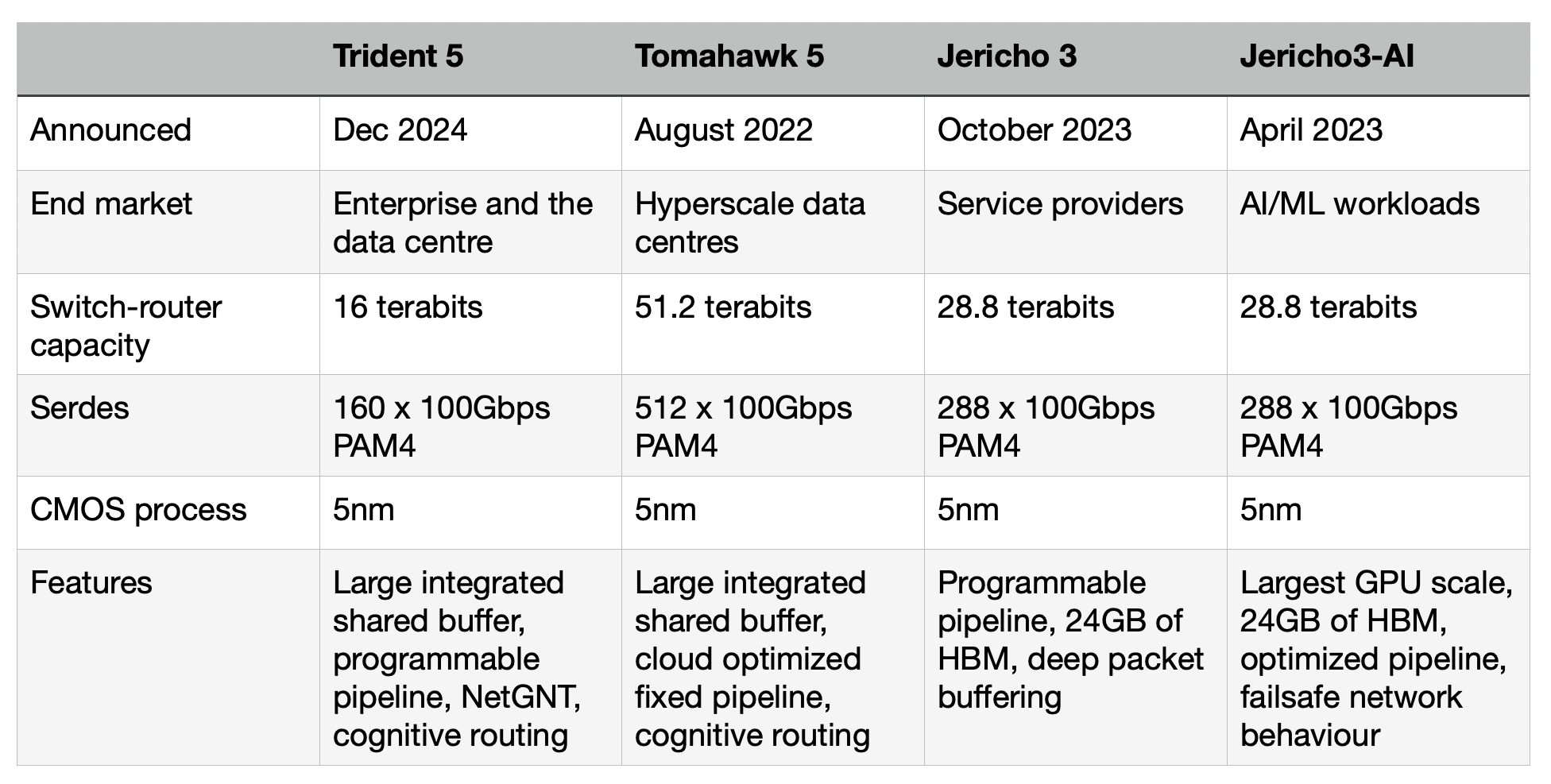
Trident family
Trident is one of Broadcom’s main three lines of networking and switch chips, the Jericho and Tomahawk being the other two.
Service providers favour the Jericho family for high-end IP routing applications. The Ethernet switch router chip’s features include a programmable pipeline and off-chip store for large traffic buffering and look-up tables.
The latest Jericho 3, the 28.8 terabits-per-sec (Tbps) Jericho 3, was announced in September. Broadcom launched the first family device, the Jericho3-AI, earlier this year; a chip tailored for AI networking requirements.
In contrast, Broadcom’s Tomahawk Ethernet network switch family addresses the data centre operators’ needs. The Tomahawk has a relatively simple fixed packet-processing pipeline to deliver the highest switching capacity. The Tomahawk 5 has a capacity of 51.2 terabits and includes 512, 100-gigabit PAM4 serialiser-deserializer (serdes).
“The big hyperscalers want maximum bandwidth and maximum radix [switches],” says Grindley. “The hyperscalers have a pretty simple fabric network and do everything else themselves.”
The third family, the Trident Ethernet switch chips, is popular for enterprise applications. Like the Jericho, the Trident has a programmable pipeline to address enterprise networking tasks such as Virtual Extensible LAN (VXLAN), tunnelling protocols, and segment routing (SRv6).
The speeds and timelines of the various Tomahawk and Trident chips are shown in the chart.

Trident 5-X12
The Trident 5-X12 is implemented using a 5nm CMOS process and has a capacity of 16 terabits. The chip’s input-output includes 160, 100-gigabit PAM4 serdes. These are the serdes that Broadcom introduced with the Tomahawk 5.
The first chip of each new generation of Trident usually has the highest capacity and is followed by lower-capacity devices tailored to particular markets.
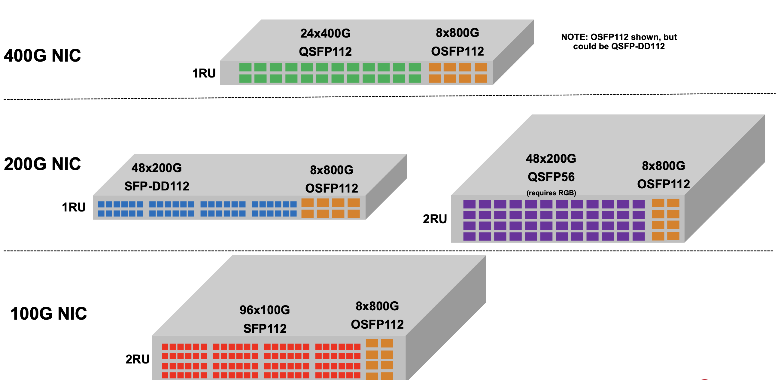
Trident 5 is aimed at top-of-rack switch applications. Typically, 24 or 48 ports of the top-of-rack switch are used for downlinks to connect to servers, while 4 or 8 are used for higher-capacity uplinks (see diagram).
The Trident 5 can support 48 ports of 200 gigabits for the downlinks and eight 800 gigabit for the uplinks. To support 800-gigabit interfaces, the chip uses eight 100-gigabit serdes and an one-chip 800-gigabit media access controller (MAC). Other top-of-rack switch configurations are shown in the diagram.
Currently, 400-gigabit network interface cards are used for demanding applications such as machine learning. Trident5 is also ready to transition to 800-gigabit network interface cards.
Another Tomahawk feature the Trident 5 has adopted is cognitive routing, a collection of congestion management techniques for demanding machine-learning workloads.
One of the techniques is global load balancing. Previous Trident devices supported dynamic load balancing, where the hardware could see the congested port and adapt in real-time. However, such a technique gives no insight into what happens further along the flow path. “If I knew that, downstream, somebody else was congested, then I could make a smarter decision,” says Grindley. Global load balancing does just this. It sends notification to the routing chips upstream that there is congestion so they can all work together.
Another cognitive routing feature is drop congestion notification. Here, packets dropped due to congestion are captured such that what is sent is only their header data and where the packet was dropped. This mechanism improves flow completion times compared to normal packet loss, which is costly for machine-learning workloads.
Trident 5, like its predecessor, Trident 4, has a heterogeneous pipeline of tile types. The tiles contain static random-access memory (SRAM), ternary content-addressable memory (TCAM) or arithmetic logic units. The tiles allow multiple look-ups or actions in parallel at each stage in the pipeline.

Broadcom has a compiler that maps high-level packet-processing functions to its pipeline in the NPL programming language. The latency through the device stays constant, however the packet processing is changed, says Grindley.
Trident 5’s NetGNT inference engine is a new pipeline resource for higher-level traffic patterns. “NexGNT looks at things not at a packet-by-packet level, but across time and the overall packet flow through the network,” says Grindley.
The NetGNT
Until now system architects and network operation centre staff have defined a set of static rules written in software to uncover and treat suspicious packet flows. “A pre-coded set of rules is limited in its ability to catch higher-level traffic patterns,” says Grindley.
When Broadcom started the Trident 5 design, its engineers thought a neural network approach could be used. “We knew it would be useful if you had something that looked at a higher level, and we knew neural networks could do this kind of task,” says Grindley.
The neural network sits alongside the existing traffic analysis logic. Information such as packet headers, or data already monitored and generated by the pipeline, can be fed to the neural network to assess the traffic patterns.
“It sits there and looks for high-level patterns such as the start of a denial of service attack” says Grindley.
Training
The neural network is trained using supervised learning. A human expert must create the required training data and train the model using supervised learning. The result is a set of weights loaded onto the Trident 5’s neural network.

When the neural network is triggered, i.e. when it identifies a pattern of interest, the Trident 5 must decide what it should do. The chip can drop the packets or change the quality of service (QoS). The device can also drop a packet while creating a mirror packet containing headers and metadata. This can then be sent to a central analyser at the network operations centre to perform higher-level management algorithms.
Performance
The Trident 5 chip is now sampling. Broadcom says there is no performance data as end customers are still to train and run live traffic through the Trident 5’s inference engine.
“What it can do for them depends on getting good data and then running the training,” says Grindley. “Nobody has done this yet.”
Will the inference engine be used in other Broadcom networking chips?
“It depends on the market,” says Grindley. “We can replicate it, just like taking IP from the Tomahawk where appropriate.”

Juniper bolsters its MX routers with packet processing ASIC
Juniper Networks has developed its next-generation packet processor, a single-chip package that includes 3D-stacked high-bandwidth memory. The device’s first use will be to enhance three of Juniper’s flagship MX series edge routers.
The company has also announced software for the 5G cellular standard that separates the control and user planes, known as CUPS, and two new MX-series platforms that will use the company’s universal chassis.

The company’s MX series edge routers were first introduced in 2007. “The MX is a platform that is at the heart of our service provider customers globally, as well as a number of our cloud provider and enterprise customers,” says Sally Bament, Juniper’s vice president of service provider marketing (pictured).
The latest enhancements will provide the MX edge router customers with another decade of support to meet their evolving service requirements, says Bament.
 Source: Gazettabyte, Juniper Networks
Penta silicon
Juniper’s latest single-chip packet processor has a 500 gigabit-per-second (Gbps) duplex throughput and is implemented using a 16nm CMOS process. This compares to Juniper’s existing 120Gbps duplex 65nm CMOS Trio packet processor that is a four-device chipset that powers the MX platforms and was unveiled in 2009. The single packaged chip with its 3D-stacked memory reduces packaging by 83 per cent compared to the four-chip Trio chipset.
The Penta is being readied for the advent of 400–gigabit client-side interfaces and features 50Gbps serialiser/ deserialisers (serdes).
Juniper will use the Penta Silicon on its latest MPC10E linecard that has a capacity of 1.5 terabit-per-second (Tbps). The linecard will be used to enhance its MX240, MX480 and MX960 edge routers. The current MPC7E linecard, powered by the Trio, has a 480Gbps capacity.
 The MPC10E linecard showing the client interface options and the three Penta ICs. Source: Juniper Networks
The company highlights the Penta programmability, enabling it to accommodate new emerging routing protocols.
The custom chip is also the first with hardware acceleration for Layer 2 MACsec and Layer 3 IPsec encryption protocols, claims Juniper.
“The benefit [of hardware acceleration] is that you don’t have to trade off encryption with processing performance and scale,” says Bament. “We can terminate thousands of IPSec sessions without any performance impact.”
The Penta also supports the FlexEthernet standard.
CUPS
Juniper claims it is the first vendor to implement CUPS, developed by the 3GPP standards body.
CUPS stands for Control and User Plane Separation of Evolved Packet Core (EPC) nodes. “By decoupling the control and user planes, you can scale them independently,” says Bament.
Such a separation brings several benefits. CUPS can be used to reduce latency by moving user plane nodes closer to the radio access network. Low latency is required to enable emerging network edge applications such as self-driving cars and virtual reality-augmented reality.
Adding more user plane nodes will also help service providers cope with the continual increase in mobile data traffic. AT&T says data in its mobile network has grown 3,600x since 2007 and it expects a further near-10x growth by 2022.
With CUPS, service providers can combine different vendors’ control plane and user plane solutions in their network. “We can now interoperate with third-party 5G control planes from vendors,” says Bament. Juniper already partners with Affirmed Networks, a virtualised 5G control plane vendor.
Service providers also have a choice for the user plane itself: they can use physical hardware such as Juniper’s MX platforms or virtualised user plane solutions from third-party vendors, or both solutions in their networks.
Universal chassis
Juniper has also unveiled two additional MX platforms that use its universal chassis announced a year ago. Having a universal chassis simplifies inventory management and operational costs.
The common chassis is already used for Juniper’s PTX packet transport core routers and its QFX switches for the data centres. At the time of the universal chassis launch, Juniper said it would also support MX linecards.
The two new MX edge routers using the universal platform are the MX10008 and MX10016. The 13 rack unit (13RU) MX10008 has a 19.2-terabit capacity while the 21RU MX10016 doubles it to 38.4 terabits.
White boxes
The leading service providers are increasingly promoting the adoption of white boxes yet the Juniper announcement includes all the classical elements of traditional telecom equipment: chassis, line cards and custom silicon.
“There is certainly a trend towards white-box implementations and certainly customers are buying software from us and putting it on white boxes,” says Bament. “But it is limited; there is still a way to go in terms of broad adoption.”
Bament points to Juniper’s software-based vMX virtual edge routing solution as well as its CUPS software to show that it is pursuing virtual network function solutions as well as enhancing its MX platforms to benefit service providers’ existing investments.
The two MX platforms will be available in the second half of this year, the Penta ASIC-based MPC10E line card for the MX240, MX480 and MX960 will be available in the first quarter of next year while the CUPS software is due in the first half of 2019.
Further information
Juniper Trio white paper, click here
EZchip packs 100 ARM cores into one networking chip
 The Tile-Mx100. Source: EZchip
- The industry's first detailed chip featuring 100, 64-bit ARM cores
- The Tile-Mx devices will perform control plane processing and data plane processing
- The 100-core chip will have 100 Gigabit Ethernet ports and support 200 Gigabit duplex traffic
EZchip has detailed the industry's first 100-core processor. Dubbed the Tile-Mx100, the processor will be the most powerful of a family of devices aimed at such applications as software-defined networking (SDN), network function virtualisation (NFV), load-balancing and security. Other uses include video processing and application recognition, to identify applications riding over a carrier's network.
Known for its network processors, EZchip has branched out to also include general-purpose processors following its acquisition of multicore specialist, Tilera. It now competes with such companies as Broadcom, Cavium and Intel.
What's new about the EZchip Tile-Mx100 is that it is the first such processor with 100 cache-coherent programmable CPU cores and it is by far the largest 64-bit ARM processor yet announced
EZchip's NPS network processor is a custom IC designed to maximise packet-processing performance. The Tile-Mx also targets networking but using standard ARM cores. Engineers will benefit from open source software, third-party applications and ARM development tools. "We believe the market needs a standard, open architecture," says Amir Eyal, vice president of business development at EZchip.
"A multicore standard processor tailored for networking is nothing new; numerous such processors have been available for years from several vendors," says Tom Halfhill, senior analyst at The Linley Group. "What's new about the EZchip Tile-Mx100 is that it is the first such processor with 100 cache-coherent programmable CPU cores and it is by far the largest 64-bit ARM processor yet announced."
EZchip has detail three Tile-Mx devices, the most powerful being the Tile-Mx100 that uses 100, 64-bit ARM Cortex-A53 cores. The Cortex-A53 is newer and smaller than the Cortex-A57, and has a relatively low power consumption. Handset and tablet designs are also using the ARM Cortex-A53 core. Both the A53 and A57 cores use the ARMv8-A instruction set.
"We have taken the A53 in order to put more cores on the die," says Eyal. "The idea with networking applications is that the more packets you can process in parallel, the better." A chip hosting many, smaller cores helps meet this goal.
Tile-Mx architecture
The Tile-Mx100 device will process traffic at rates up to 200 Gigabit-per-second (Gbps) rates, or 200 Gbps duplex. In contrast, EZchip's NPS family of devices has a roadmap with a traffic processing performance of 400 Gbps to 800 Gbps duplex.
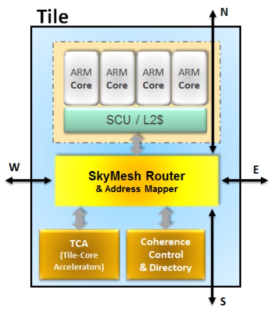
The Tile-Mx uses a two-level architecture. The 100 cores are partitioned into 25 processing clusters or tiles, each comprising four ARM cores that share network acceleration hardware and level-2 cache memory. Each tile also features router hardware, part of the chip's interconnect network that handles the tile's input/ output (I/O) requirements.
 Source: EZchip
"The key technology for the Tile-Mx architecture is the interconnect that enables 100 CPUs to be connected in a coherent manner," says Jag Bolaria, principal analyst at The Linley Group.
"There are five different networks [part of the mesh] that interconnect the 100 cores in parallel, preventing bottlenecks and contention," says Eyal. The mesh also ensures that each core can talk to the chip's I/O and to the memory. The mesh is a fifth iteration, having been improved with each generation of chip design, says Eyal, and has a total bandwidth of 25 Terabits.
The mesh also implements cache coherency, an important aspect of multi-processor design that ensures that cache memory is updated when accessed by any of the cores without needing to introduce idle states first.
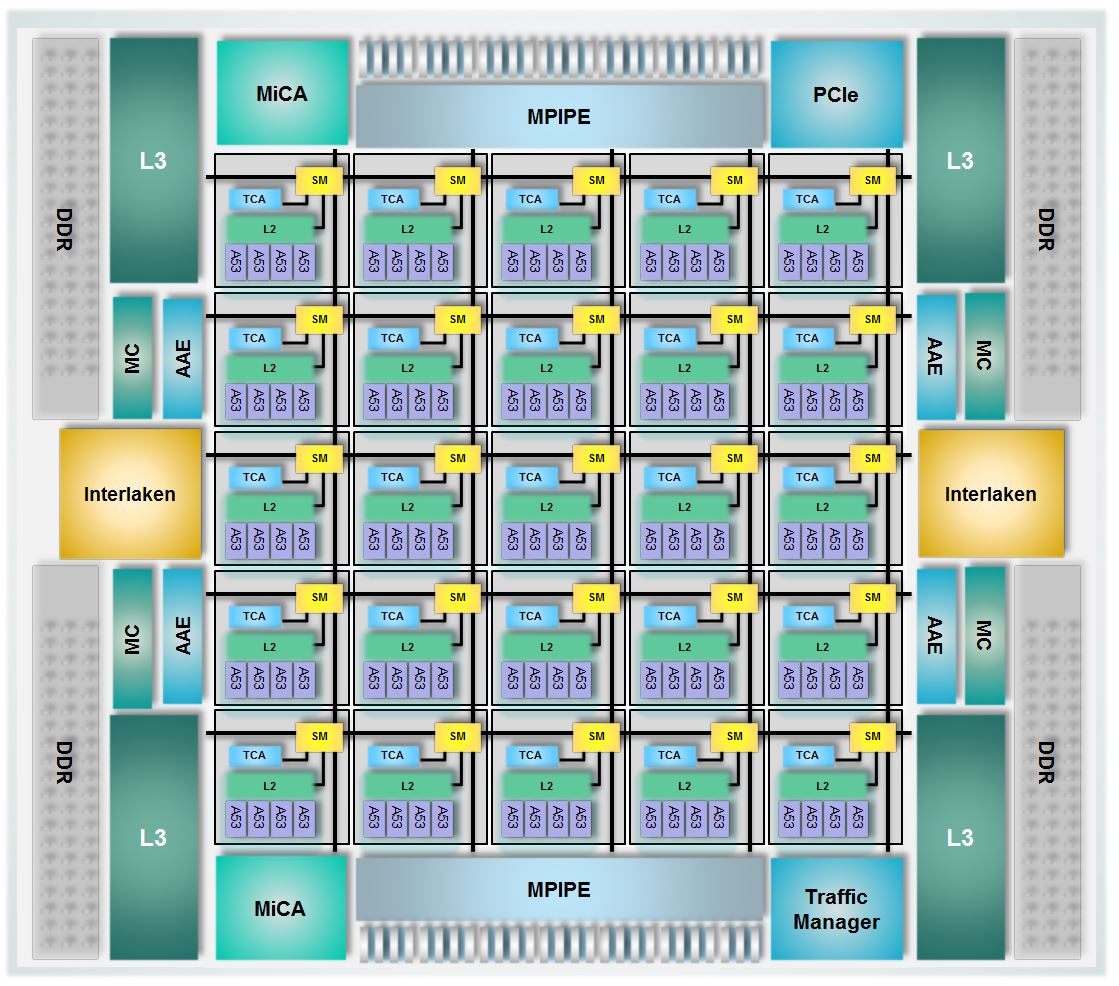
Other chip features include a traffic manager, essentially the one used for EZchip's NPUs, which prioritises traffic, allocates bandwidth and prevents packet loss. There are also hardware units (see MiCA blocks in main chip diagram), developed by Tilera, which do preliminary packet classification before presenting the packets to the cores.
The chip's I/O includes 1, 10, 25, 40, 50 and 100 Gigabit Ethernet interfaces, the Interlaken interface and PCI Express, used to connect the chip to a host processor such as an Intel x86 microprocessor.
The idea with networking applications is that the more packets you can process in parallel, the better
EZchip is not detailing the device's interface mix or such metrics as the chip's pin-count, clock speed or power consumption. However, EZchip says the chip's power consumption will be under 100W.
When a packet is presented to the chip, it is assigned to a core which processes it to completion before sending it typically to the I/O. For the programmer, the 100-core device appears as a single processor; it is the hardware on-chip that handles the details, sending an incoming packet to the next free core.
Ezchip shows examples of possible platforms that could use the Tile-Mx.
One is a 1-rack-unit-high pizza box in the data centre used to deliver virtual network functions. Such a NFV server would benefit from the Tile-Mx's hardware-accelerated table look-ups, packet classification and packet flow management in and out of the device. Another design example is using the device for an intelligent network interface card (NIC) in a standard Intel x86-based server.
The two other Tile-Mx family devices will use 36 and 64 Cortex-A53 cores. First Tile-Mx samples are expected in the second half of 2016.
Multicore trends
The Linley Group says that despite the unprecedented 100 ARM cores, EZchip's family of device faces competition. Moreover, the trend to increase core-count has its limits.
EZchip is already shipping a 72-core processor it acquired from Tilera although the device is not ARM-based. And Cavium's largest processor has 48 cores, says Halfhill. Broadcom's largest processor has only 20 cores, but those CPUs are quad-threaded, so the processor can handle up to 80 packet streams. "Not quite as many as the Tile-Mx100, but it is in the same ballpark," says Halfhill.
"Keep in mind that Tile-Mx100 production is about two years out; a lot can happen in two years," adds Halfhill.
According to Bolaria, multicore designs are good for applications that are highly parallelised such as packet processing and deep packet processing. But NPUs are better if all that is being done is packet processing.
"Many cores is not particularly good for applications that need good single-thread performance," says Bolaria. "This is where [an Intel] Xeon will shine — for applications such as high-performance computing, simulations and algorithms."
Coherent interconnects also limit CPU scaling, says Bolaria. Tile-Mx gets around the interconnect limitation by clustering four ARM cores into a tile, so that effectively 25 nodes only are connected. "With more nodes, it becomes difficult to maintain cache coherency and performance," says Bolaria.
Another limitation is partitioning applications into smaller chunks for execution on 100 cores. Some tasks are serial by nature and cannot benefit from parallel processing. "Amdahl’s law limits performance gains from adding more CPUs," says Bolaria.