Taking a unique angle to platform design

- A novel design based on a vertical line card shortens the trace length between an ASIC and pluggable modules.
- Reducing the trace length improves signal integrity while maintaining the merits of using pluggables.
- Using the vertical line card design will extend for at least two more generations the use of pluggables with Ethernet switches.
The travelling salesperson problem involves working out the shortest route on a round-trip to multiple cities. It’s a well-known complex optimisation problem.
Novel design that shortens the distance between an Ethernet switch chip and the front-panel optics
Systems engineers face their own complex optimisation problem just sending an electrical signal between two points, connecting an Ethernet switch chip to a pluggable optical module, for example.
Sending the high-speed signal over the link with sufficient fidelity for its recovery requires considerable electronic engineering design skills. And with each generation of electrical signalling, link distances are getting shorter.
In a paper presented at the recent ECOC show, held in Basel, consultant Chris Cole, working with Yamaichi Electronics, outlined a novel design that shortens the distance between an Ethernet switch chip and the front-panel optics.
The solution promises headroom for two more generations of high-speed pluggables. “It extends the pluggable paradigm very comfortably through the decade,” says Cole.
Since ECOC, there are plans to standardise the vertical line card technology in one or more multi-source agreements (MSAs), with multiple suppliers participating.
“This will include OSFP pluggable modules as well as QSFP and QSFP-DD modules,” says Cole.
Shortening links
Rather than the platform using stacked horizontal line cards as is common today, Cole and Yamaichi Electronics propose changing the cards’ orientation to the vertical plane.
Vertical line cards also enable the front-panel optical modules to be stacked on top of each other rather than side-by-side. As a result, the pluggables are closer to the switch ASIC; the furthest the high-speed electrical signalling must travel is three inches (7.6cm). The most distant span between the chip and the pluggable with current designs is typically nine inches (22.8cm).
“The reason nine inches is significant is that the loss is high as we reach 200 gigabits-per-second-per-lane and higher,” says Cole.
Current input-output proposals
The industry is pursuing several approaches to tackle such issues as the issues associated with high-speed electrical signalling and also input-output (I/O) bandwidth density.
One is to use twinaxial cabling instead of electrical traces on a printed circuit board (PCB). Such ‘Twinax’ cable has a lower loss, and its use avoids developing costly advanced-material PCBs.
Other approaches involve bringing the optics closer to the Ethernet switch chip, whether near-packaged optics or the optics and chip are co-packaged together. These approaches also promise higher bandwidth densities.
Cole’s talk focussed on a solution that continues using pluggable modules. Pluggable modules are a low-cost, mature technology that is easy to use and change.
However, besides the radio frequency (RF) challenges that arise from long electrical traces, the I/O density of pluggables is limited due to the size of the connector, while placing up to 36 pluggables on the 1 rack unit-high (1RU) front panel obstructs the airflow used for cooling.
Platform design
Ethernet switch chips double their capacity every two years. Their power consumption is also rising; Broadcom’s latest Tomahawk 5 consumes 500W.
The power supply a data centre can feed to each platform has an upper limit. It means fewer cards can be added to a platform if the power consumed per card continues to grow.
The average power dissipation per rack is 16kW, and the limit is around 32kW, says Cole. This refers to when air cooling is used, not liquid cooling.
He cites some examples.
A rack of Broadcom’s 12.8-terabit Tomahawk 3 switch chip – either with 32, 1RU or 16, 2RU cards with two chips per card – and associated pluggable optics consume over 30kW.
A 25.6-terabit Tomahawk 4-based chassis supports 16 line cards and consumes 28kW. However, using the recently announced Tomahawk 5, only eight cards can be supported, consuming 27KW.
“The takeaway is that rack densities are limited by power dissipation rather than the line card’s rack unit [measure],” says Cole.
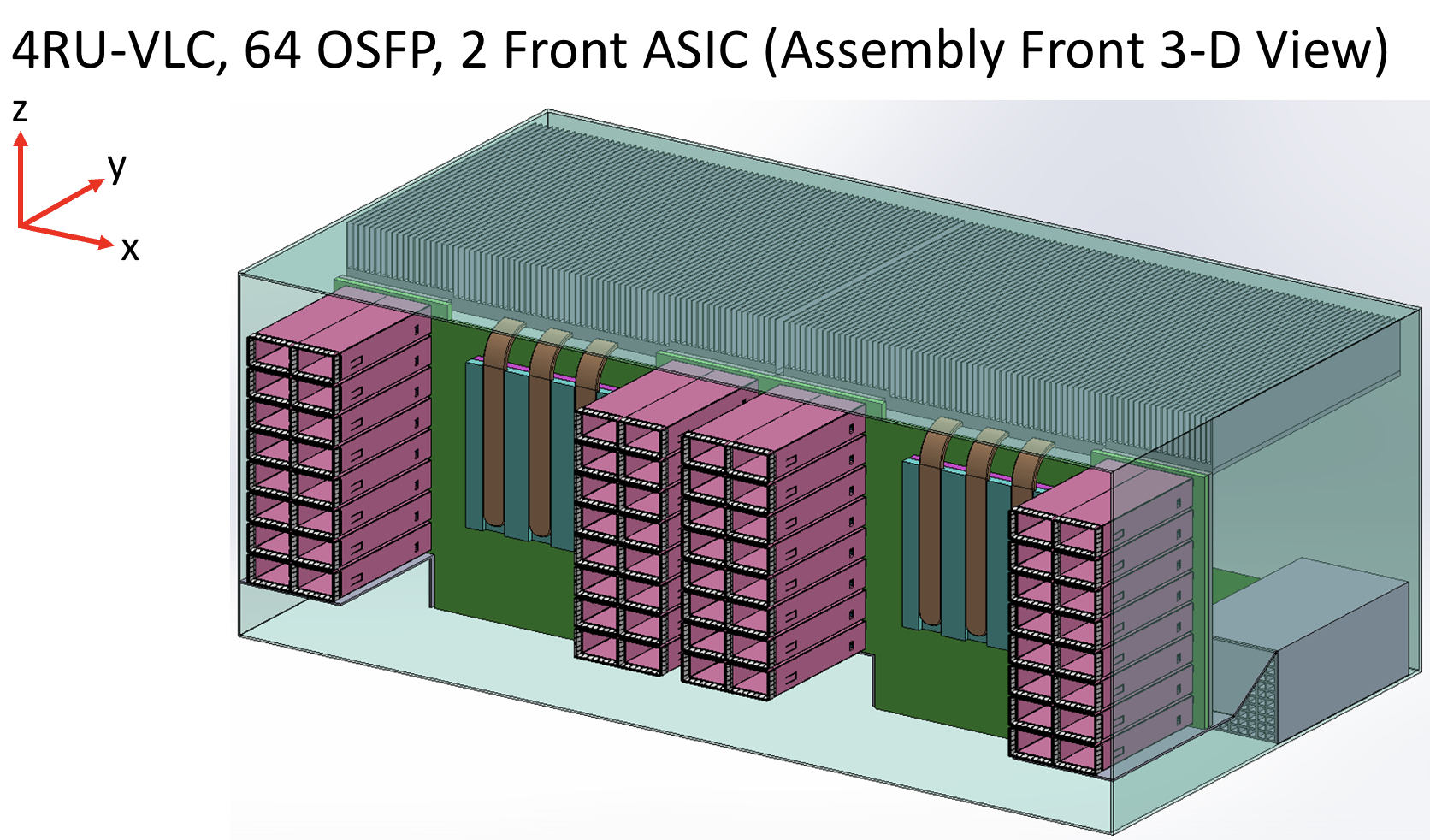
Vertical line card
The vertical line card design is 4RU high. Each card supports two ASICs on one side and 64 cages for the OSFP modules on the other.
A 32RU chassis can thus support eight vertical cards or 16 ASICs, equivalent to the chassis with 16 horizontal 2RU line cards.
The airflow for the ASICs is improved, enabling more moderate air fans to be used compared to 1RU or 2RU horizontal card chassis designs. There is also airflow across the modules.
“The key change in the architecture is the change from a horizontal card to a vertical card while maintaining the pluggable orientation,” says Cole.
As stated, the maximum distance between an ASIC and the pluggables is reduced to three inches, but Cole says the modules can be arranged around the ASIC to minimise the length to 2.5 inches.
Alternatively, if the height of the vertical card is an issue, a 3RU card can be used instead, which results in a maximum trace length of 3.5 inches. “[In this case], we don’t have dedicated air intakes for the CPU,” notes Cole.
Cole also mentioned the option of a 3RU vertical card that houses one ASIC and 64 OSFP modules. This would be suitable for the Tomahawk 5. However, here the maximum trace length is five inches.
Vertical connectors
Yamaichi Electronics has developed the vertical connectors needed to enable the design.
Cole points out that, unlike a horizontal connector, a vertical one uses equal-length contacts. This is not the case for a flat connector, resulting in performance degradation since a set of contacts has to turn and hence has a longer length.
Cole showed the simulated performance of an OSFP vertical connector with an insertion loss of over 70GHz.
“The loss up to 70GHz demonstrates the vertical connector advantage because it is low and flat for all the leads,” says Cole. “So this [design] is 200-gigabit ready.”
He also showed a vertical connector for the OSFP-XD with a similar insertion loss performance.
Also shown was a comparison with results published for Twinax cables. Cole says this indicates that the loss of a three-inch PCB trace is less than the loss of the cable.
“We’ve dramatically reduced the RF maximum length, so we had solved the RF roadblock problem, and we maintain the cost-benefit of horizontal line cards,” says Cole.
The I/O densities may be unchanged, but it preserves the mature technology’s benefits. “And then we get a dramatic improvement in cooling because there are no obstructions to airflow,” says Cole.
Vladimir Kozlov, CEO of the market research firm, LightCounting, wondered in a research note whether the vertical design is a distraction for the industry gearing up for co-packaged optics.
“Possibly, but all approaches for reducing power consumption on next-generation switches deserve to be tested now,” said Kozlov, adding that adopting co-packaged optics for Ethernet switches will take the rest of the decade.
“There is still time to look at the problem from all angles, literally,” said Kozlov

Nokia adds 400G coherent modules across its platforms

Nokia is now shipping its 400-gigabit coherent multi-haul CFP2-DCO. The module exceeds the optical performance of 400ZR and ZR+ coherent pluggables.
Nokia’s CFP2-DCO product follows its acquisition of silicon photonics specialist, Elenion Technologies, in 2020.
Nokia has combined Elenion’s coherent optical modulator and receiver with its low-power 64-gigabaud (GBd) PSE-Vc coherent digital signal processor (DSP).
Nokia is also adding coherent pluggables across its platform portfolio.
“Not just optical transport and transponder platforms but also our IP routing portfolio as well,” says Serge Melle, director of product marketing, IP-optical networking at Nokia.
“This [amplifier and filter] allows for much better optical performance,”
“This [amplifier and filter] allows for much better optical performance,”
Melle is an optical networking industry veteran. He joined Nokia two years ago after a 15-year career at Infinera. Melle started at Pirelli in 1995 when it was developing a 4×2.5-gigabit wavelength-division multiplexing (WDM) system. In between Pirelli and Infinera, Melle was at Nortel Networks during the optical boom.
400ZR, ZR+ and the multi-haul CFP2-DCO
The CFP2-DCO’s optical performance exceeds that of the QSFP-DD and OSFP form factors implementing 400ZR and ZR+ but is inferior to line-card coherent transponders used for the most demanding optical transport applications.
The 400ZR coherent OIF standard transmits a 400-gigabit wavelength up to 120km linking equipment across data centres. Being a standard, 400ZR modules are interoperable.
The ZR+ adds additional transmission speeds – 100, 200 and 300-gigabits – and has a greater reach than ZR. ZR+ is not a standard but there is the OpenZR+ multi-source agreement (MSA).
Implementing 400ZR and ZR+ coherent modules in a QSFP-DD or OSFP module means they can be inserted in client-side optics’ ports on switches and routers.
The OIF did not specify a form factor as part of the 400ZR standard, says Melle, with the industry choosing the QSFP-DD and OSFP. But with the modules’ limited power dissipation, certain modes of the coherent DSP are turned off, curtailing the feature set and the reach compared to a CFP2-DCO module.
The modules also have physical size restrictions.
“You don’t have enough thermal budget to put an optical amplifier inside the QSFP-DD package,” says Melle. “So you are left with whatever power the DWDM laser outputs through the modulator.” This is -7dBm to -10dBm for 400ZR and ZR+ optics, he says.
The CFP2-DCO is larger such that the DSP modes of encryption, OTN client encapsulation, LLDP snooping (used to gather data about attached equipment), and remote network monitoring (RMON) can be enabled.
The CFP2-DCO can also house an optical amplifier and tunable filter. The filter reduces the out-of-band optical signal-to-noise ratio (OSNR) thereby increasing the module’s sensitivity. “This [amplifier and filter] allows for much better optical performance,” says Melle. A 400-gigabit multi-haul module has a 0dBm optical output power, typically.
The different transceiver types are shown in the table.
Nokia’s paper at the recent OFC virtual conference and exhibition detailed how its 400-gigabit multi-haul CFP2-DCO achieved a reach of 1,200km.
The paper details the transmission of 52, 400-gigabit signals, each occupying a 75GHz channel, for a total capacity of 20.8 terabits-per-second (Tbps).
Melle stresses that the demonstration was more a lab set-up than a live network where a signal goes through multiple reconfigurable optical add-drop multiplexers (ROADMs) and where amplifier stages may not be equally spaced.
That said, the CFP2-DCO’s reach in such networks is 750km, says Nokia.
IP-optical integration
Having coherent pluggables enables 400 Gigabit Ethernet (400GbE) payloads to be sent between routers over a wide area network, says Nokia.
“Given this convergence in form factor, with the QSFP-DD and ZR/ ZR+, you can now do IP-optical integration, putting coherent optics on the router without sacrificing port density or having locked-in ports,” says Melle.
Nokia is upgrading its IP and optical portfolio with coherent pluggables.
“In the routers, ZR/ ZR+, and in transponders not only the high-performance coherent optics – the [Nokia] PSE-Vs [DSP] – but also the CFP2-DCO multi-haul,” says Melle. “The 400-gigabit multi-haul is also going to be supported in our routers.”
Accordingly, Nokia has developed two sets of input-output (I/O) router cards: one supporting QSFP-DDs suited for metro-access applications, and the second using CFP2-DCO ports for metro and regional networks.
The choice of cards adds flexibility for network operators; they no longer need to have fixed CFP2-DCO slots on their router faceplates, whether they are used or not. But being physically larger, there are fewer CFP2-DCO ports than QSFP-DD ports on the I/O cards.
While the QSFP-DD MSA initially defined the module with a maximum power dissipation of 14.5W, a coherent QSFP-DD module consumes 18-20W. Dissipating the heat generated by the modules is a challenge.
Nokia’s airflow cooling is simplified by placing a module on both sides of the line card rather than stacking two CFP2-DCOs, one on top of the other.
Nokia is adding its CFP2-DCO to its 1830 optical transport portfolio. These include its PSI-M compact modular systems, the PSS transponder systems and also its PSS-x OTN switching systems.
The 400ZR/ZR+ module will be introduced with all its routing platforms this summer – the 7250 IXR, 7750 SR, 7750 SR-s, and the 7950 XRS, whereas the CFP2-DCO will be added to its 7750 and 7950 series later this year.
Nokia will source the 400ZR/ZR+ from third parties as well as from its optical networks division.
Its routers use QSFP-DD form-factor for all 400GbE ports and this is consistent for most router vendors in the industry. “Thus, our use and supply of 400ZR/ZR+ pluggable DCOs will focus on the QSFP-DD form-factor,” says Melle. However, the company says it can offer the OSFP form-factor depending on demand.
Network planning study
Nokia published a paper at OFC on the ideal coherent solution for different applications.
For metro aggregation rings with 4-5 nodes and several ROADM pass-throughs, using ZR+ modules is sufficient. Moreover, using the ZR+ avoids any loss in router port density.
For metro-regional core applications, the ZR+’s optical performance is mostly insufficient. Here, the full 400-gigabit rate can not be used but rather 300 gigabit-per-second (Gbps) or even 200Gbps to meet the reach requirements.
Using a 400-gigabit multi-haul pluggable on a router might not match the density of the QSFP-DD but it enables a full 400-gigabit line rate.
For long-haul, the CFP2-DCO’s performance is “reasonable”, says Nokia, and this is where high-performance transponders are used.
What the OFC paper argues is that there is no one-size-fits-all solution, says Melle.
800-Gigabit coherent pluggables
Traditionally, the IEEE has defined short-reach client-side optics while the OIF defines coherent standards.
“If we want this IP-optical convergence continuing in the next generation of optics, those two worlds are going to have to collaborate more closely,” says Melle.
That’s because when a form-factor MSA will be defined, it will need to accommodate the short-reach requirements and the coherent optics. If this doesn’t happen, says Melle, there is a risk of a new split occuring around the IP and optical worlds.
The next generation of coherent pluggables will also be challenging.
All the vendors got together in 2019 and said that 400ZR was just around the corner yet the modules are only appearing now, says Melle.
The next jump in pluggable coherent optics will use a symbol rate of 90-130GBd.
“That is very much the cutting-edge so it brings back the optics as a critical enabling technology, and not just optics but the packaging,” concludes Melle.

Inphi unveils first 800-gigabit PAM-4 signal processing chip
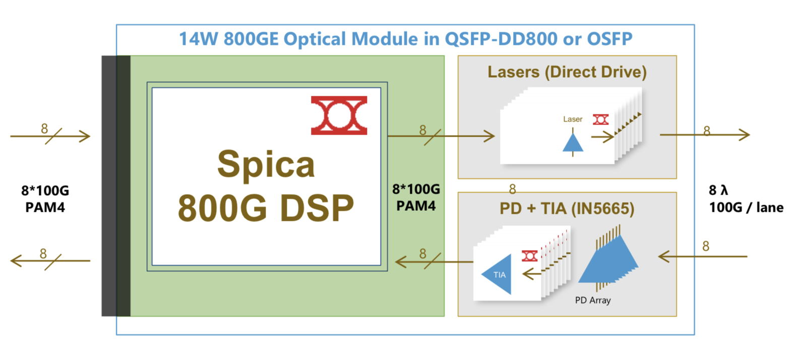
Inphi has detailed what it claims is the industry’s first digital signal processor (DSP) chip family for 800-gigabit client-side pluggable modules.
Dubbed Spica, the 4-level pulse-amplitude modulation (PAM-4) DSP family is sampling and is in the hands of customers.
The physical-layer company has also announced its third-generation Porrima family of PAM-4 DSPs for 400-gigabit pluggables.
The Porrima DSP with integrated laser driver has being made using a 7nm CMOS process; until now a 16nm CMOS has been used. Fabricating the chip using the more advanced process will reduce the power consumption of 400-gigabit module designs.
Applications
Eight-hundred-gigabit multi-source agreements (MSAs) will enable a new generation of high-speed optical transceivers to come to market.
The 800G Pluggable MSA developing optical specifications for 800-gigabit pluggable modules, is one that Inphi is promoting, while the QSFP-DD800 MSA is extending the double density form factor for 800 gigabits.

The main two markets driving a need for 800-gigabit modules are artificial intelligence (AI) and data centre switching, says Eric Hayes, senior vice president, networking interconnect at Inphi.
“AI, while still in its infancy, has all these applications and workloads that it can drive,” he says. “But one thing they have in common when we look at the data centres building large AI clusters is that they have very large data sets and lots of data flow.”
The speed of the input-output (I/O) of the AI processors used in the clusters is rising to cope with the data flows.
The second application that requires 800-gigabit modules is the advent of 25.6-terabit Ethernet switches used to network equipment within the data centre.
Inphi says there are two types of 25.6-terabit switch chips emerging: one uses 50-gigabit PAM-4 while the second uses 100-gigabit PAM-4 electrical interfaces.
“The 25.6-terabyte switch with 100-gigabit I/O is wanted for one-rack-unit (1RU) platforms,” says Hayes. “To do that, you need an 800-gigabit module.” Such switches have yet to reach the marketplace.
The first-generation AI processors used 25-gigabit non-return-to-zero (NRZ) signalling for the I/O while many of the devices shipping today use 50-gigabit PAM-4. “The latest designs that are coming to market have 100-gigabit I/O and we have the first DSP offering 100-gigabit on the host side,” says Hayes.
Spica and Porrima ICs
The Spica DSP takes 100-gigabits PAM-4 electrical signals from the host and performs retiming and pre-emphasis to generate the 100-gigabit PAM-4 signals used for modulation the optics before transmission. The laser driver is integrated on-chip.
The transmit path is a simpler design than the Porrima in that the signalling rate is the same at the input and the output. Accordingly, no gearbox circuitry is needed.
The main signal processing is performed at the receiver to recover the sent PAM-4 signals. A hybrid design is used combining analogue and digital signal processing, similar to the design used for the Porrima.
The Spica device supports 2×400-gigabit or 8×100-gigabit module designs and enables 800-gigabit or 8×100-gigabit optical interconnects. The 800-gigabit form factors used are the QSFP-DD800 and the OSFP. Inphi says both designs consume under 14W.
“The first module being built [using the Spica] is the OSFP because the end-user is demanding that, but we also have customers building QSFP-DDs,” says Hayes.
Meanwhile, Inphi’s Porrima family of devices is targeted at the 400G DR4 and 400G FR4 specifications as well as 100-gigabit module designs that use 100-gigabit PAM-4.
The two module types can even be combined when a 400-gigabit pluggable such as a QSFP-DD or an OSFP is used in breakout mode to feed four 100-gigabit modules implement using such form factors as the QSFP, uQSFP or SFP-DD.
Transitioning the Porrima to a 7nm process saves 1.5W of power, says Hayes, resulting in an 8W 400-gigabit module. The latest Porrima is sampling and is with customers.
Roadmap
Inphi says optical modules using the Spica DSP will be deployed in volume from the second half of 2021.
Before then, the DSP will be tested as part of customers’ module designs, then be integrated with the software before the complete 800-gigabit module is tested.
“There will then be interoperability testing between the modules once they become available and then small pilot networks using 800-gigabit modules will be built and tested before the go-ahead to mass deployment,” says Hayes.
All these stages will require at least a year’s work.

Acacia unveils its 400G coherent module portfolio

Acacia Communications has unveiled a full portfolio of 400-gigabit coherent optics and has provided test samples to customers, one being Arista Networks.
Delivering a complete set of modules offers a comprehensive approach to address the next phase of coherent optics, the company says.
The 400-gigabit coherent designs detailed by Acacia are implemented using the QSFP-DD, OSFP and CFP2 pluggable form factors.
Collectively, the pluggables support three performance categories: the 400ZR standard, OpenZR+ that is backed by several companies, and the coherent optics specification used for the Open ROADM multi-source agreement (MSA).
OIF-defined 400ZR standard designed for hyperscalers
“These are challenging specifications,” says Tom Williams, vice president of marketing at Acacia. “Even the 400ZR, where the objective has been to simplify the requirements.”
400ZR and OpenZR+
The OIF-defined 400ZR standard is designed for hyperscalers to enable the connection of switches or routers in data centres up to 120km apart.
The 400ZR standard takes in a 400 Gigabit Ethernet (GbE) client signal and outputs a 400-gigabit coherent signal for optical transmission.
“Hyperscaler customers want a limited subset of performance [with the ZR] because they don’t want to introduce operational complexity,” says Williams.
Acacia is implementing the 400ZR standard with two module offerings: the QSFP-DD and the OSFP.
Acacia is also a founding member of OpenZR+, the industry initiative that supports both 400ZR and extended optical performance modes. The other OpenZR+ members are NEL, Fujitsu Optical Components, Lumentum, Juniper Networks and Cisco Systems which is in the process of acquiring Acacia.
OpenZR+ supports 100GbE and its multiples (200GbE and 300GbE) input signals, not just 400GbE as used for ZR. To transmit the 200- 300- and 400GbE client signals, OpenZR+ uses quadrature phase-shift keying (QPSK), 8-ary quadrature amplitude modulation (8-QAM), and 16-QAM, respectively.
OpenZR+ also employs an enhanced forward-error correction (oFEC) used for the Open ROADM specification and delivers improved dispersion compensation performance.
“OpenZR+ is not just about going further but also being able to offer more functionality than 400ZR,” says Williams.
Acacia is implementing OpenZR+ using the QSFP-DD and OSFP form factors.
Open ROADM
The Open ROADM specification is the most demanding of the three modes and is targeted for use by the telecom operators. Here, a CFP2-DCO module is used due to its greater power envelope. And while the Open ROADM optics is aimed at telcos, the CFP2-DCO also supports OpenZR+ and 400ZR modes.
“The telcos are not as focussed on [face plate] density,” says Williams. “The CFP2-DCO has a higher output and is not limited to just Ethernet but also multiplexed client signals and OTN.”
Since line cards already use CFP2-DCO modules, the Open ROADM module enables a system upgrade. Existing line cards using the 200-gigabit CFP2-DCO may not support 400GbE client signals but with the Open ROADM CFP2’s higher symbol rate, it offers enhanced reach performance.
This is because the Open ROADM CFP2-DCO uses a 64 gigabaud (GBd) symbol rate enabling a 200-gigabit signal to be transmitted using QPSK modulation. In contrast, 32GBd is used for the existing 200-gigabit CFP2-DCOs requiring 16-QAM. Using QPSK rather than 16-QAM enables better signal recovery.
There is also an interoperability advantage to the new CFP2-DCO in that its 200-gigabit mode is compliant with the CableLabs specification.
All three designs – 400ZR, OpenZR+ and Open ROADM – use Acacia’s latest 7nm CMOS Greylock low-power coherent digital signal processor (DSP).
This is the company’s third-generation low-power DSP following on from its Sky and Meru DSPs. The Meru DSP is used in existing 32GBd 100/ 200-gigabit CFP2-DCOs.
3D stacking
Acacia has spent the last year and a half focusing on packaging, using techniques from the semiconductor industry to ensure the pluggable form factors can be made in volume.
The higher baud rate used for the 400-gigabit coherent modules means that the electronic ICs and the optics need to be closely coupled. “Moving up the baud rate means that the interconnection between the [modulator] driver [chip] and the modulator can become a limiting factor,” says Williams.
Acacia is not detailing the 3D design except to say that the Greylock DSP, its silicon-photonics photonic integrated circuit (PIC), and the modulator driver and trans-impedance amplifier (TIA) are all assembled into one package using chip-stacking techniques. The chip is then mounted onto a printed circuit board much like a BGA chip, resulting in a more scalable process, says Acacia.
“We have taken the DSP and optics and turned that into an electronic component,” says Williams. “Ultimately, we believe it will lead to improvements in reliability using this volume-repeatable process.”
Acacia says its modules will undergo qualification during most of this year after which production will ramp.
No one module design will be prioritised, says Williams: “There are a lot of benefits of doing all three, leveraging a lot of common elements.”

Optical module trends: A conversation with Finisar
Finisar demonstrated recently a raft of new products that address emerging optical module developments. These include:
- A compact coherent integrated tunable transmitter and receiver assembly
- 400GBASE-FR8 and -LR8 QSFP-DD pluggable modules and a QSFP-DD active optical cable
- A QSFP28 100-gigabit serial FR interface
- 50-gigabit SFP56 SR and LR modules
Rafik Ward, Finisar’s general manager of optical interconnects, explains the technologies and their uses.
Compact coherent
Finisar is sampling a compact integrated assembly that supports 100-gigabit and 200-gigabit coherent transmission.
The integrated tunable transmitter and receiver assembly (ITTRA), to give it its full title, includes the optics and electronics needed for an analogue coherent optics interface.
The 32-gigabaud ITTRA includes a tunable laser, optical amplifier, modulators, modulator drivers, coherent mixers, a photo-detector array and the accompanying trans-impedance amplifiers, all within a gold box. “An entire analogue coherent module in a footprint that is 70 percent smaller than the size of a CFP2 module,” says Ward. The ITTRA's power consumption is below 7.5W.
 Rafik WardFinisar says the ITTRA is smaller than the equivalent integrated coherent transmitter-receiver optical sub-assembly (IC-TROSA) design being developed by the Optical Internetworking Forum (OIF).
“We potentially could take this device and enable it to work in that [IC-TROSA] footprint,” says Ward.
Using the ITTRA enables higher-density coherent line cards and frees up space within an optical module for the coherent digital signal processor (DSP) for a CFP2 Digital Coherent Optics (CFP2-DCO) design.
Ward says the CFP2 is a candidate for a 400-gigabit coherent pluggable module along with the QSFP-DD and OSFP form factors. “All have their pros and cons based on such fundamental things as the size of the form factor and power dissipation,” says Ward.
But given coherent DSPs implemented in 7nm CMOS required for 400 gigabit are not yet available, the 100 and 200-gigabit CFP2 remains the module of choice for coherent pluggable interfaces.
 The demonstration of the ITTRA implementing a 200-gigabit link using 16-QAM at OFC 2018. Source: Finisar
400 gigabits
Finisar also demonstrated its first 400-gigabit QSFP-DD pluggable module products based on the IEEE standards: the 2km 400GBASE-FR8 and the 10km 400GBASE-LR8. The company also unveiled a QSFP-DD active optical cable to link equipment up to 70m apart.
The two QSFP-DD pluggable modules use eight 50-gigabit PAM-4 electrical signal inputs that are modulated onto eight lasers whose outputs are multiplexed and sent over a single fibre. Finisar chose to implement the IEEE standards as its first QSFP-DD products as they are low-power and lower risk 400-gigabit solutions.
The alternative 2km 400-gigabit design, developed by the 100 Lambda MSA, is the 400G-FR4 that uses four 100-gigabit optical lanes. “This has some risk elements to it such as the [PAM-4] DSP and making 100-gigabit serial lambdas work,” says Ward. “We think the -LR8 and -FR8 are complementary and could enable a fast time-to-market for people looking at these kinds of interfaces.”
The QSFP-DD active optical cable may have a reach of 70m but typical connections are 20m. Finisar uses its VCSEL technology to implement the 400-gigabit interface. At the OFC show in March, Finisar demonstrated the cable working with a Cisco high-density port count 1 rack-unit switch.
I sometimes get asked by customers what is the best way to get to higher-density 100 gigabit. I point to the 400-gigabit DR4.
QSFP28 FR
Finisar also showed it 2km QSFP28 optical module with a single wavelength 100-gigabit PAM-4 output. The QSFP28 FR takes four 25 gigabit-per-second electrical interfaces and passes them through a gearbox chip to form a 50-gigabaud PAM-4 signal that is used to modulate the laser.
The QSFP28 FR is expected to eventually replace the CWDM4 that uses four 25-gigabit wavelengths multiplexed onto a single fibre. “The end-game is to get a 100-gigabit serial module,” says Ward. “This module represents the first generation of that.”
Finisar is also planning a 500m QSFP28 DR. The QSFP28 DR and FR will work with the 500m IEEE 400GBASE-DR4 that has four outputs, each a fibre carrying a 100-gigabit PAM-4 signal, with the -DR4 outputs interfacing with up to four FR or DR modules.
“I sometimes get asked by customers what is the best way to get to higher-density 100 gigabit,” says Ward. “I point to the 400 gigabit DR4, even though we call it a 400-gigabit part, it is also a 4x100-gigabit DR solution.”
Ward says that the 500m reach of the DR is sufficient for the vast majority of links in the data centre.
SFP56 SR and LR
Finisar has also demonstrated two SFP56 modules: a short reach (SR) version that has a reach of 100m over OM4 multi-mode fibre and the 10km LR single-mode interface. The SR is VSCEL-based while the LR uses a directly-modulated distributed feedback laser.
The SFP is deployed widely at speeds up to and including 10 gigabits while the 25-gigabit SFP shipments are starting to ramp. The SFP56 is the next-generation SFP module with a 50-gigabit electrical input and a 50-gigabit PAM-4 optical output.
The SFP56 will be used for several applications, says Finisar. These include linking servers to switches, connecting switches in enterprise applications, and 5G wireless applications.
Finisar says its 50 and 100 gigabit-per-lane products will likely be released throughout 2019, in line with the industry. “The 8-channel devices will likely come out at least a few quarters before the 4-channel devices,” says Ward.
400ZR will signal coherent’s entry into the datacom world
- 400ZR will have a reach of 80km and a target power consumption of 15W
- The coherent interface will be available as a pluggable module that will link data centre switches across sites
- Huawei expects first modules to be available in the first half of 2020
- At OFC, Huawei announced its own 250km 400-gigabit single-wavelength coherent solution that is already being shipped to customers
Coherent optics will finally cross over into datacom with the advent of the 400ZR interface. So claims Maxim Kuschnerov, senior R&D manager at Huawei.
 Maxim Kuschnerov400ZR is an interoperable 400-gigabit single-wavelength coherent interface being developed by the Optical Internetworking Forum (OIF).
The 400ZR will be available as a pluggable module and as on-board optics using the COBO specification. The IEEE is also considering a proposal to adopt the 400ZR specification, initially for the data-centre interconnect market. “Once coherent moves from the OIF to the IEEE, its impact in the marketplace will be multiplied,” says Kuschnerov.
But developing a 400ZR pluggable represents a significant challenge for the industry. “Such interoperable coherent 16-QAM modules won’t happen easily,” says Kuschnerov. “Just look at the efforts of the industry to have PAM-4 interoperability, it is a tremendous step up from on-off keying.”
Despite the challenges, 400ZR products are expected by the first half of 2020.
400ZR use cases
The web-scale players want to use the 400ZR coherent interface to link multiple smaller buildings, up to 80km apart, across a metropolitan area to create one large virtual data centre. This is a more practical solution than trying to find a large enough location that is affordable and can be fed sufficient power.
Once coherent moves from the OIF to the IEEE, its impact in the marketplace will be multiplied
Given how servers, switches and pluggables in the data centre are interoperable, the attraction of the 400ZR is obvious, says Kuschnerov: “It would be a major bottleneck if you didn't have [coherent interface] interoperability at this scale.”
Moreover, the advent of the 400ZR interface will signal the start of coherent in datacom. Higher-capacity interfaces are doubling every two years or so due to the webscale players, says Kuschnerov, and with the advent of 800-gigabit and 1.6-terabit interfaces, coherent will be used for ever-shorter distances, from 80km to 40km and even 10km.
At 10km, volumes will be an order of magnitude greater than similar-reach dense wavelength-division multiplexing (DWDM) interfaces for telecom. “Datacom is a totally different experience, and it won’t work if you don’t have a stable supply base,” he says. “We see the ZR as the first step combining coherent technology and the datacom mindset.”
Data centre players will plug 400ZR modules into their switch-router platforms, avoiding the need to interface the switch-router to a modular, scalable DWDM platform used to link data centres.
The 400ZR will also find use in telecom. One use case is backhauling residential traffic over a cable operator’s single spans that tend to be lossy. Here, ZR can be used at 200 gigabits - using 64 gigabaud signalling and QPSK modulation - to extend the reach over the high-loss spans. Similarly, the 400ZR can also be used for 5G mobile backhaul, aggregating multiple 25-gigabit streams.
Another application is for enterprise connectivity over distances greater than 10km. Here, the 400ZR will compete with direct-detect 40km ER4 interfaces.
Having several use cases, not just data-centre interconnect, is vital for the success of the 400ZR. “Extending ZR to access and metro-regional provides the required diversity needed to have more confidence in the business case,” says Kuschnerov.
The 400ZR will support 400 gigabits over a single wavelength with a reach of 80km, while the target power consumption is 15W.
The industry is still undecided as to which pluggable form factor to use for 400ZR. The two candidates are the QSFP-DD and the OSFP. The QSFP-DD provides backward compatibility with the QSFP+ and QSFP28, while the OSFP is a fresh design that is also larger. This simplifies the power management at the expense of module density; 32 OSFPs can fit on a 1-rack-unit faceplate compared to 36 QSFP-DD modules.
The choice of form factor reflects a broader industry debate concerning 400-gigabit interfaces. But 400ZR is a more challenging design than 400-gigabit client-side interfaces in terms of trying to cram optics and the coherent DSP within the two modules while meeting their power envelopes.
The OSFP is specified to support 15W while simulation results published at OFC 2018 suggest that the QSFP-DD will meet the 15W target. Meanwhile, the 15W power consumption will not be an issue for COBO on-board optics, given that the module sits on the line card and differs from pluggables in not being confined within a cage.
Kuschnerov says that even if it proves that only the OSFP of the two pluggables supports 400ZR, the interface will still be a success given that a pluggable module will exist that delivers the required face-plate density.
400G coherent
Huawei announced at OFC 2018 its own single-wavelength 400-gigabit coherent technology for use with its OptiX OSN 9800 optical and packet OTN platform, and it is already being supplied to customers.
The 400-gigabit design supports a variety of baud rates and modulation schemes. For a fixed-grid network, 34 gigabaud signalling enables 100 gigabits using QPSK, and 200 gigabits using 16-QAM, while at 45 gigabaud 200 gigabits using 8-QAM is possible. For flexible-grid networks, 64 gigabaud is used for 200-gigabit transmission using QPSK and 400 gigabits using 16-QAM.
Huawei uses an algorithm called channel-matched shaping to improve optical performance in terms of data transmission and reach. This algorithm includes such techniques as pre-emphasis, faster-than-Nyquist, and Nyquist shaping. According to Kuschnerov, the goal is to squeeze as much capacity out of a network’s physical channel so that advanced coding techniques such as probabilistic constellation shaping can be used to the full. For Huawei’s first 400-gigabit wavelength solution, constellation shaping is not used but this will be added in its upcoming coherent designs.
Huawei has already demonstrated the transmission of 400 gigabits over 250km of fibre. “Current generation 400G-per-lambdas does not enable long-haul or regional transmission so the focus is on shorter reach metro or data-centre-interconnect environments,” says Kuschnerov.
When longer reaches are needed, Huawei can offer two line cards, each supporting 200 gigabits, or a single line card hosting two 200-gigabit modules. The 200-gigabits-per-wavelength is achieved using 64 gigabaud and QPSK modulation, resulting in a 2,500km reach.
Up till now, such long-haul distances have been served using 100-gigabitwavelengths. Now, says Kuschnerov, 200 gigabit at 64 gigabaud is becoming the new norm in many newly built networks while the 34 gigabaud 200 gigabit is being favoured in existing networks based on a 50GHz grid.
Oclaro makes available its EMLs and backs 400G-FR4
Lumentum’s plan to acquire Oclaro for $1.8 billion may have dominated the news at last month’s OFC show held in San Diego, but it was business as usual for Oclaro with its product and strategy announcements.
 Adam Carter, chief commercial officer (pictured), positions Oclaro’s announcements in terms of general industry trends.
“On the line side, everywhere there are 100-gigabit and 200-gigabit wavelengths, you will see that transition to 400 gigabit and 600 gigabit,” he says. “And on the client side, you have 100 gigabit going to 400 gigabit.”
400G-FR
Oclaro announced it will offer the QSFP56-DD module implementing 400-FR4, the four-wavelength 400-gigabit 2km client-side interface. The 400G-FR4 is a design developed by the 100G Lambda MSA.
“This [QSFP-DD FR4] will enable our customers, particularly network equipment manufacturers, to drive 400 gigabit up to 36 ports in a one-rack-unit [platform],” says Carter.
Oclaro has had the required optical components - its 53-gigabaud lasers and high-end photo-detectors - for a while. What Oclaro has lacked is the accompanying 4-level pulse amplitude modulation (PAM-4) gearbox chip to take the 8x50 gigabits-per-second electrical signals and encode them into four 50-gigabaud ones.
The chips have now arrived for testing and if the silicon meets the specs, Oclaro will deliver the first modules to customers later this year.
Oclaro chose the QSFP-DD first as it expects the form factor to sell in higher volumes but it will offer the 400G-FR4 in the OSFP module.
Certain customers prefer the OSFP, in part because of its greater power-handling capabilities. “Some people believe that the OSFP’s power envelope gives you a little bit more freedom,” he says. “There is still a debate in the industry whether the QSFP-DD will be able to do long-reach [80km data centre interconnect] types of products.”
Oclaro says its transmit and receive optical sub-assemblies (TOSAs and ROSAs) are designed to fit within the more demanding QSFP-DD such they will also suit the OSFP.
If people want to buy the [EML] chips and do next-generation designs, they can come to Oclaro
EMLs for sale
Oclaro has decided to sell its electro-absorption modulated lasers (EMLs), capable of 25, 50 and 100-gigabit speeds.
“If people want to buy the chips and do next-generation designs, they can come to Oclaro for some top-end single-mode chipsets that we have developed for our own use,” says Carter.
Oclaro's EMLs are used for both coarse wavelength-division multiplexing (CWDM) and the tighter LAN-WDM wavelength grid based client-side interfaces and are available in uncooled and cooled packages.
Until now the company only sold its 25-gigabit directly modulated lasers (DMLs). “We have been selling [EMLs] strategically to one very large customer who consigns them to a manufacturer,” says Carter.
The EMLs are being made generally available due to demand. “There are not many manufacturers of this chip in the world,” says Carter, adding that the decision also reflects an evolving climate for business models.
5G and cable
Oclaro claims it is selling the industry’s first 10-gigabit tunable SFP+ operating over industrial temperature (I-temp) ranges: -40 to 85oC. There are two tunable variants spanning 40km and 80km, both supporting up to 96 dense WDM (DWDM) channels on a fibre. The module was first announced at OFC 2017.
Oclaro says cable networks and 5G wireless will require the I-temp tunable SFP+.
The cable industry’s adoption of a distributed access architecture (DAA) brings fibre closer to the network’s edge and splits part of the functionality of the cable modem termination system (CMTS) - the remote PHY - closer to the residential units. This helps cable operators cope with continual traffic growth and their facilities becoming increasingly congested with equipment. Comcast, for example, says it is seeing an annual growth in downstream traffic (to the home) of 40-50 percent.
The use of tunable SFP+ modules boost the capacity that can be sent over a fibre, says Carter. But the tunable SFP+ modules are now located at the remote PHY, an uncontrolled temperature environment.
For 5G, the 10Gbps tunables will carry antenna traffic to centralised base stations. Carter points out that the 40km and 80km reach of the tunable SFP+ will not be needed in all geographies but in China, for example, the goal is to limit the number of central offices such that the distances are greater.
Oclaro also offers an I-temp fixed-wavelength 25-gigabit SFP28 LR module. “It is lower cost than the tunable SFP+ so if you need 10km [for mobile fronthaul], you would tend to go for this transceiver,” says Carter.
Also unveiled is an optical chip combining a 1310nm distributed feedback laser (DFB) laser and a Mach-Zehnder modulator. “The 1310nm device will be used in certain applications inside the data centre,” says Carter. “There are customers that are looking at using PAM-4 interfaces for short-reach connections between leaf and spine switches.” The device will support 50-gigabit and 100-gigabit PAM-4 wavelengths.
Line-side optics
Oclaro announced it is extending its integrated coherent transmitter and integrated coherent receiver to operate in the L-band. The coherent optical devices support a symbol rate of up to 64 gigabaud to enable 400-gigabit and 600-gigabit wavelengths.
Telcos want to use the L-band alongside the C-band to effectively double the capacity of a fibre.
Also announced by Oclaro at OFC was a high-bandwidth co-packaged modulator driver, an indium phosphide-based Mach-Zehnder modulator.
Oclaro was part of the main news story at last year’s OFC when Ciena announced it would share its 400-gigabit WaveLogic Ai coherent digital signal processor (DSP) with three module makers: Oclaro, Lumentum and NeoPhotonics. Yet there was no Oclaro announcement at this year’s OFC regarding the transponder.
Carter says the WaveLogic Ai transponder is sampling and that it has been demonstrated to customers and used in several field trials: “It is still early right now with regard volume deployments so there is nothing to announce yet."
DustPhotonics reveals its optical transceiver play
A start-up that has been active for a year has dropped its state of secrecy to reveal it is already shipping its first optical transceiver product.
The company, DustPhotonics, is backed by private investors and recently received an undisclosed round of funding that will secure the company’s future for the next two years.
Product plans
DustPhotonics' first product is the multi-mode 100m-reach 100GBASE-SR4 QSFP28. The company will launch its first 400-gigabit optical modules later this year.
 Ben Rubovitch
“We probably are going to be one of the first to market with [400-gigabit] QSFP-DD and OSFP multi-mode solutions,” says Ben Rubovitch, CEO of DustPhotonics.
The start-up has developed 50 gigabit-per-lane technology required for higher-speed modules such as the QSFP56, QSFP-DD and OSPF pluggables. The QSFP-DD form factor is designed to be backwards compatible with the QSFP and QSFP28 and is backed by the likes of Facebook and Cisco, while the OSFP is a new form factor supported by Google and switch maker Arista Networks.
DustPhotonics chose the 4-lane 25-gigabit QSFP28 to prove the working of its 50 gigabit-per-lane technology. “The reason we did that is that the PAM-4 chipsets weren’t ready when we started,” says Rubovitch. “So we invested the first year solving the production issues and the optical interface and used the QSFP28 as the platform.”
The challenge with a 50 gigabit-per-lane optical interface is that the photo-detector aperture used is smaller. “So on our QSFP28 we used a small photo-detector to prove the optical solution,” says Rubovitch.
The start-up is now developing faster speed multi-mode designs: a 200-gigabit QSFP56 pluggable, a 400-gigabit QSFP-DD implementing the 400GBASE-SR8 standard and a similar active optical cable variant; products that it hopes to sample in the second quarter of this year. This will be followed by similar SR8 implementations using the OSFP.
 DustPhotonics' optical product roadmap. Source: Gazettabyte/ DustPhotonics.
DustPhotonics is also adapting its optical packaging technology to support single-mode designs: the 500m IEEE 400GBASE-DR4 and the 2km 400G-FR4, part of the 100G Lambda multi-source agreement (MSA). Both the DR4 and FR4 designs use 100-gigabit optical lanes.
Technology
Rubovitch says that despite the many optical transceiver players and the large volumes of modules now manufactured, pluggable optics remain expensive. “The front panel of a top-of-rack switch [populated with modules] costs ten times more than the switch itself,” he says.
DustPhotonics has tackled the issue of cost by simplifying the module’s bill of materials and the overall manufacturing process.
The start-up buys the lasers and electronic ICs needed and adds its own free-space optics for both multi-mode and single-mode transceiver designs. “It is all plastic-molded so we don’t use any glass types or any integrated lasers and that simplifies much of the process,” says Rubovitch. Indeed, he claims the design reduces the bill of materials of its transceivers by between 30 and 50 percent.
The front panel of a top-of-rack switch [populated with modules] costs ten times more than the switch itself
DustPhotonics has also developed a passive alignment process. “We have narrowed the one accurate step - where we align the optics - to one machine,” says Rubovitch. “This compares to two steps ‘accurate’ and one step ‘align’ for active alignment.” Active alignment for a QSFP28 module takes ten minutes, he says, whereas DustPhotonics’ passive alignment process takes under a minute per module.
“There is also a previous manufacturing stage where we place the VCSELs and photo-detectors on a substrate itself and we don’t need accuracy here, unlike other solutions,” he says.
The overall result is a simpler, more cost-effective design. “We are already manufacturing in a volume production line and we see the numbers and how competitive we are, and it is going to create an even larger advantage at 400 gigabits,” says Rubovitch.
DustPhotonics’ passive alignment process takes under a minute per module
What next?
DustPhotonics is also developing embedded optics, where the optics are placed next to an ASIC, and even in-package designs where the optics and ICs are co-packaged.
Rubovitch says such technologies will be needed because of the very high power 100-gigabit electrical transceivers consume on a switch chip, for example, as well the silicon area they require; precious silicon real estate needed to cope with the ever-increasing packet-processing demands. “Bringing the optics very close [to the chip] can help solve those issues for the switch providers,” he says.
As Rockley Photonics’ CEO, Andrew Rickman, observed recently, combining optics with the switch silicon has long been discussed yet has still to be embraced by the switch chip makers. This explains why Rockley developed its own switch ASIC to demonstrate a complete in-packaged reference design.
Rubovitch agrees that the concept of optics replacing electrical interfaces has long been spoken of but that hasn’t happened due to copper speeds continuing to advance. There is already a 100 gigabit-per-lane solution that will meet the demands of the next generation of switch designs, he says: “It really depends on what is going to be the next leap: 200 gigabits or 400-gigabits.”
Using optics to replace electrical interfaces could come with the advent of 25 terabit switch silicon or maybe the generation after. “Or maybe something in between: 25 terabit solutions will start to move gradually to a more packaged solution or at least closer on-board optics,” concludes Rubovitch.
The many paths to 400 gigabits
The race is on to deliver 400-gigabit optical interfaces in time for the next-generation of data centre switches expected in late 2018.
The industry largely agrees that a four-wavelength 400-gigabit optical interface is most desirable yet alternative designs are also being developed.
Optical module makers must consider such factors as technical risk, time-to-market and cost when choosing which design to back.
 Rafik Ward, FinisarUntil now, the industry has sought a consensus on interfaces, making use of such standards bodies as the IEEE to serve the telecom operators.
Now, the volumes of modules used by the internet giants are such that they dictate their own solutions. And the business case for module makers is sufficiently attractive that they are willing to comply.
Another challenge at 400 gigabits is that there is no consensus regarding what pluggable form factor to use.
“There is probably more technical risk in 400 gigabits than any of the historical data-rate jumps we have seen,” says Rafik Ward, vice president of marketing at Finisar.
Shrinking timeframes
One-hundred-gigabit interfaces are now firmly established in the marketplace. It took several generations to achieve the desired module design. First, the CFP module was used, followed by the CFP2. The industry then faced a choice between the CFP4 and the QSFP28 form factors. The QSFP28 ended up winning because the 100-gigabit module met the price, density and performance expectations of the big users - the large-scale data centre players, says Paul Brooks, director of strategy for lab and production at Viavi Solutions.
“The QSFP28 is driving huge volumes, orders of magnitude more than we see with the other form factors,” he says.
There is probably more technical risk in 400 gigabits than any of the historical data-rate jumps we have seen
It was the telcos that initially drove 100-gigabit interfaces, as with all the previous interface speeds. Telcos have rigorous optical and physical media device requirements such that the first 100-gigabit design was the 10km 100GBASE-LR4 interface, used to connect IP routers and dense wavelength-division multiplexing (DWDM) equipment.
 Paul Brooks, Viavi Solutions
But 100 gigabits is also the first main interface speed influenced by the internet giants. “One-hundred-gigabit volumes didn’t take that inflection point until we saw the PSM4 and CWDM4 [transceiver designs],” says Brooks. The PSM4 and CWDM4 are not IEEE specification but multi-source agreements (MSAs) driven by the industry.
The large-scale data centre players are now at the forefront driving 400 gigabits. They don’t want to wait for three generations of modules before they get their hands on an optimised design. They want the end design from the start.
“There was a lot of value in having iterations at 100 gigabits before we got to the high-volume form factor,” says Ward. “It will be more challenging with the compressed timeframe for 400 gigabits.”
Datacom traffic is driven by machine-to-machine communication whereas telecom is driven by consumer demand. Machine-to-machine has twice the growth rate.
Data centre needs
Brandon Collins, CTO of Lumentum, explains that the urgency of the large-scale data centre players for 400 gigabits is due to their more pressing capacity requirements compared to the telcos.
 Brandon Collings, LumentumDatacom traffic is driven by machine-to-machine communication whereas telecom is driven by consumer demand. “Machine-to-machine has twice the growth rate,” says Collins. “The expectation in the market - and everything in the market aligns with this - is that the datacom guys will be adopting in volume much sooner than the telecom guys.”
The data centre players require 400-gigabit interfaces for the next-generation 6.4- and 12.8-terabit top-of-rack switches in the data centre.
“The reason why the top-of-rack switch is going to need 400-gigabit uplinks is because server speeds are going to go from 25 gigabits to 50 gigabits,” says Adam Carter, chief commercial operator for Oclaro.
A top-of-rack switch’s downlinks connect to the servers while the uplinks interface to larger ‘spine’ switches. For a 36-port switch, if four to six ports are reserved for uplinks and the remaining ports are at 50 gigabits-per-second (Gbps), 100-gigabit uplinks cannot accommodate all the traffic.
The 6.4-terabit and 12.8-terabit switches are expected towards the end of next year. These switches will be based on silicon such as Broadcom’s Tomahawk-III, start-up Innovium’s Teralynx and Mellanox’s Spectrum-2. All three silicon design examples use 50-gigabit electrical signalling implemented using 4-level pulse-amplitude modulation (PAM-4).
PAM-4, a higher order modulation scheme, used for the electrical and optical client interfaces is another challenge at 400-gigabit. The use of PAM-4 requires a slight increase in bandwidth, says Brooks, and introduces a loss that requires compensation using forward error correction (FEC). “Four-hundred-gigabits is the first Ethernet technology where you always have FEC on,” he says.
CFP8
The modules being proposed for 400-gigabit interfaces include the CFP8, the Octal Small Form Factor (OSFP) and the double-density QSFP (QSFP-DD) pluggable modules. COBO, the interoperable on-board optics standard, will also support 400-gigabit interfaces.
The QSFP-DD is designed to be backward compatible with the QSFP and QSFP28 pluggables while the OSFP is a new form factor.
At OFC earlier this year, several companies showcased 400-gigabit CFP8-based designs.
NeoPhotonics detailed a CFP8 implementing 400GBASE-LR8, the IEEE 802.3bs Task Force’s 10km specification that uses eight wavelengths, each at 50-gigabit PAM4. Finisar announced two CFP8 transceivers: the 2km 400GBASE-FR8 and the 10km 400GBASE-LR8. Oclaro also announced two CFP8 designs: the 10km 400GBASE-LR8 and an even longer reach 40km version.
The 400-gigabit CFP8 is aimed at traditional telecom applications such as linking routers and transport equipment.
NeoPhotonics’ CFP8 is not yet in production and the company says it is not seeing a present need. “There is probably a short window before it gets replaced by the QSFP-DD or, on the telecom side, the OSFP,” says Ferris Lipscomb, vice president of marketing at NeoPhotonics.
Finisar expects its 400-gigabit CFP8 products by the year-end, while Oclaro is sampling its 10km 400-gigabit CFP8.
But the large-scale data centre players are not interested in the CFP8 which they see as too bulky for the data centre. Instead, Amazon, Facebook, and equipment vendor Cisco Systems are backing the higher-density QSFP-DD, while Google and Arista Networks are proponents of the OSFP.
“The data centre players don’t need IEEE standardisation, they need the lowest cost and the most compact form factor,” says Lumentum’s Collings.
QSFP-DD and OSFP
To achieve 400 gigabits, the QSFP-DD has twice the number of electrical lanes of the QSFP, going from four to eight, while each lane’s speed is doubled to 56Gbps using PAM-4.
“Time and time again we have heard with the QSFP-DD that plugging in legacy modules is a key benefit of that technology,” says Scott Sommers, group product manager at Molex and a co-chair of the QSFP-DD MSA. The power envelope of the QSFP-DD is some 12W.
 Yasunori Nagakubo, Fujitsu Optical ComponentsYasunori Nagakubo, director of marketing at Fujitsu Optical Components also highlights the high-density merits of the QSFP-DD. Up to 36 ports can fit on the front panel of a one-rack-unit (1RU) box, enabling a throughput of 14.4 terabits.
In contrast, the OSFP has been designed with a fresh sheet of paper. The form factor has a larger volume and surface area compared to the QSFP-DD and, accordingly, has a power envelope of some 16W. Up to 32 OSFP ports can fit on a 1RU front panel.
“The QSFP-DD is a natural evolution of the QSFP and is used for switch-to-switch interconnect inside the data centre,” says Robert Blum, director of strategic marketing and business development at Intel’s silicon photonics product division. He views the OSFP as being a more ambitious design. “Obviously, you have a lot of overlap in terms of applications,” says Blum. “But the OSFP is trying to address a wider segment such as coherent and also be future proofed for 800 gigabits.”
“A lot of people are trying to make everything fit inside a QSFP-DD but, after all, the OSFP is still a bigger form factor which is easier for different components to fit in,” says Winston Way, CTO, systems at NeoPhotonics. Should a 400-gigabit design meet the more constrained volume and power requirements of the QSFP-DD, the design will also work in an OSFP.
The consensus among the module makers is that neither the QSFP-DD nor the OSFP can be ignored and they plan to back both.
This [400 gigabits] may be the last hurrah for face-plate pluggables
“We have been in this discussion with both camps for quite some time and are supporting both,” says Collings. What will determine their relative success will be time-to-market issues and which switch vendors produces the switch with the selected form factors and how their switches sell. “Presumably, switches are bought on other things than which pluggable they elected to use,” says Collings.
Is having two form factors an issue for Microsoft?
“Yes and no,” says Brad Booth, principal network architect for Microsoft’s Azure Infrastructure and chair of the COBO initiative. “I understand why the QSFP-DD exists and why the OSFP exists, and both are the same reason why we started COBO.”
COBO will support 400-gigabit interfaces and also 800 gigabits by combining two modules side-by-side.
Booth believes that 400-gigabit pluggable module designs face significant power consumption challenges: “I’ve been privy to data that says this is not as easy as many people believe.”
 Brad Booth, MicrosoftIf it were only 400-gigabit speeds, it is a question of choosing one of the two pluggable modules and running with it, he says. But for future Ethernet speeds, whether it is 800 gigabits or 1.6 terabits, the design must be able to meet the thermal environment and electrical requirements.
“I do not get that feeling when I look at anything that is a face-plate pluggable,” says Booth. “This [400 gigabits] may be the last hurrah for face-plate pluggables.”
Formats
There are several 400-gigabit interface specifications at different stages of development.
The IEEE’s 802.3bs 400 Gigabit Ethernet Task Force has defined four 400 Gigabit specifications: a multi-mode fibre design and three single-mode interfaces.
The 100m 400GBASE-SR16 uses 16 multi-mode fibres, each at 25Gbps. The -SR16 has a high fibre count but future 400-gigabit multi-mode designs are likely to be optimised. One approach is an eight-fibre design, each at 50Gbps. And a four-fibre design could be developed with each fibre using coarse wavelength-division multiplexing (CWDM) carrying four 25-gigabit wavelengths.
The expectation is that at OFC 2018 next March, many companies will be demonstrating their 400-gigabit module designs including four-wavelength ones
The three single-mode IEEE specifications are the 500m 400GBASE-DR4 which uses four single-mode fibres, each conveying a 100-gigabit wavelength, and the 2km 400GBASE-FR8 and 10km 400GBASE-LR8 that multiplex eight wavelengths onto a single-mode fibre, each wavelength carrying a 50-gigabit PAM-4 signal.
The 2km and 10km IEEE specifications use a LAN-WDM spacing scheme and that requires tight wavelength control and hence laser cooling. The standards also use the IEEE CDAUI-8 electrical interface that supports eight 50-gigabit PAM-4 signals. The -FR8 and -LR8 standards are the first 400-gigabit specifications being implemented using the CFP8 module.
A new initiative, the CWDM8 MSA, has been announced to implement an alternative eight-wavelength design based on CWDM such that laser cooling is not required. And while CWDM8 will also use the CDAUI-8 electrical interface, the signals sent across the fibre are 50-gigabit non-return-to-zero (NRZ). A retimer chip is required to convert the input 50-gigabit PAM-4 electrical signals into 50-gigabit NRZ before being sent optically.
 Robert Blum, IntelProponents of the CWDM8 MSA see it as a pragmatic solution that offers a low-risk, timely way to deliver 400-gigabit interfaces.
“When we looked at what is available and how to do an optical interface, there was no good solution that would allow us to meet those timelines, fit the power budget of the QSFP-DD and be at the cost points required for data centre deployment,” says Intel’s Blum. Intel is one of 11 founding companies backing the new MSA.
A disadvantage of the MSA is that it requires eight lasers instead of four, adding to the module’s overall cost.
“Making lasers at eight different wavelengths is not a trivial thing,” says Vivek Rajgarhia, senior vice president and general manager, lightwave at Macom.
This is what the 100G Lambda MSA aims to address with its four 100-gigabit wavelength design over duplex fibre. This can be seen as a four-wavelength CWDM complement to the IEEE’s 400GBASE-DR4 500m specification.
 Vivek Rajgarhia, Macom
The first 400-gigabit standard the MSA is developing is the 400G-FR4, a 2km link that uses a CDAUI-8 interface and an internal PAM4 chip to create the 100-gigabit PAM-4 signals that are optically multiplexed onto a fibre.
The large-scale data centre players are the main drivers of four-wavelength 400-gigabit designs. Indeed, two large-scale data centre operators, Microsoft and Alibaba, have joined the 100G Lambda MSA.
“People think that because I work at Microsoft, I don’t talk to people at Google and Facebook,” says Booth. “We may not agree but we do talk.
“My point to them was that we need a CWDM4 version of 400 gigabits; the LAN-WDM eight-wavelength is a non-starter for all of us,” says Booth. “If you talk to any of the big end users, they will tell you it is a non-starter. They are waiting for the FR4.”
“Everyone wants 400 gigabit - 4x100-gigabit, that is what they are looking for,” says Rajgarhia.
If companies adopt other solutions it is purely a time-to-market consideration. “If they are going for intermediate solutions, as soon as there is 400 gigabits based on 100-gigabit serial, there is no need for them, whether it is 200-gigabit or 8x50-gigabit modules,” says Rajgarhia.
At the recent ECOC 2017 show, Macom demonstrated a 100-gigabit single-wavelength solution based on its silicon photonics optics and its 100-gigabit PAM-4 DSP chip. MultiPhy also announced a 100-gigabit PAM-4 chip at the show and companies are already testing its silicon.
The expectation is that at OFC 2018 next March, many companies will be demonstrating their 400-gigabit module designs including four-wavelength ones.
Fujitsu Optical Components says it will have a working four-wavelength 400-gigabit module demonstration at the show. “Fujitsu Optical Components favours a 4x100-gigabit solution for 400 gigabits instead of the alternative eight-wavelength solutions,” says Nagakubo. “We believe that eight-wavelength solutions will be short lived until the 4x100-gigabit design becomes available.”
The roadmap is slipping and slipping because the QSFP-DD is hard, very hard
Challenges and risk
“Everyone understands that, ultimately, the end game is the QSFP-DD but how do we get there?” says Viavi’s Brooks.
He describes as significant the challenges involved in developing a four-wavelength 400-gigabit design. These include signal integrity issues, the optics for 100-gigabit single wavelengths, the PAM-4 DSP, the connectors and the ‘insanely hot and hard’ thermal issues.
“All these problems need to be solved before you can get the QSFP-DD to a wider market,” says Brooks. “The roadmap is slipping and slipping because the QSFP-DD is hard, very hard.”
Lumentum’s Collins says quite a bit of investment has been made to reduce the cost of existing 100-gigabit CWDM4 designs and this investment will continue. “That same technology is basically all you need for 400 gigabits if you can increase the bandwidth to get 50 gigabaud and you are using a technology that is fairly linear so you can switch from NRZ to PAM-4 modulation.”
In other words, extending to a 400-gigabit four-wavelength design becomes an engineering matter if the technology platform that is used can scale.
Microsoft’s Booth is also optimistic. He does not see any challenges that suggest that the industry will fail to deliver the 400-gigabit modules that the large-scale data centre players require: “I feel very confident that the ecosystem will be built out for what we need.”
Module companies backing the most technically-challenging four-wavelength designs face the largest risk, yet also the greatest reward if they deliver by the end of 2018 and into 2019. Any slippage and the players backing alternative designs will benefit.
How the 400-gigabit market transpires will be ‘very interesting’, says Finisar’s Ward: “It will be clear who executes and who does not.”
Oclaro’s 400-gigabit plans
Adam Carter, Oclaro’s chief commercial officer, discusses the company’s 400-gigabit and higher-speed coherent optical transmission plans and the 400-gigabit client-side pluggable opportunity.
Oclaro showcased its first coherent module that uses Ciena’s WaveLogic Ai digital signal processor at the ECOC show held recently in Gothenburg.
 Adam CarterOclaro is one of three optical module makers, the others being Lumentum and NeoPhotonics, that signed an agreement with Ciena earlier this year to use the system vendor’s DSP technology and know-how to bring coherent modules to market. The first product resulting from the collaboration is a 5x7-inch board-mounted module that supports 400-gigabits on a single-wavelength.
The first WaveLogic Ai-based modules are already being tested at several of Oclaro’s customers’ labs. “They [the module samples] are very preliminary,” says Adam Carter, the chief commercial officer at Oclaro. “The really important timeframe is when we get towards the new year because then we will have beta samples.”
DSP developments
The coherent module is a Ciena design and Carter admits there isn’t going to be much differentiation between the three module makers’ products.
“We have some of the key components that sit inside that module and the idea is, over time, we would design in the rest of the componentry that we make that isn’t already in there,” says Carter. “But it is still going to be the same spec between the three suppliers.”
The collaboration with the module makers helps Ciena promote its coherent DSP to a wider market and in particular China, a market where its systems are not deployed.
Over time, the scope for differentiation between the three module makers will grow. “It [the deal] gives us access to another DSP chip for potential future applications,” says Carter.
Here, Oclaro will be the design authority, procuring the DSP chip for Ciena before adding its own optics. “So, for example, for the [OIF’s] 400G ZR, we would ask Ciena to develop a chip to a certain spec and then put our optical sub-assemblies around it,” says Carter. “This is where we do believe we can differentiate.”
Oclaro also unveiled at ECOC an integrated coherent transmitter and an intradyne coherent receiver optical sub-assemblies using its indium phosphide technology that operate at up to 64 gigabaud (Gbaud).
We expect to see 64Gbaud optical systems being trialed in 2018 with production systems following at the end of next year
A 64Gbaud symbol rate enables a 400-gigabit wavelength using 16-ary quadrature amplitude modulation (16-QAM) and a 600-gigabit wavelength using 64-QAM.
Certain customers want such optical sub-assemblies for their line card designs and Oclaro will also use the building blocks for its own modules. The devices will be available this quarter. “We expect to see 64Gbaud optical systems being trialed in 2018 with production systems following at the end of next year and the beginning of 2019,” says Carter.
Oclaro also announced that its lithium niobate modulator supporting 400-gigabit single wavelengths is now in volume production. “Certain customers do have their preferences when it comes to first designs and particularly for long-reach systems,” says Carter. “Lithium niobate seems to be the one people go with.”
400-gigabit form factors
Oclaro did not make any announcements regarding 400-gigabit client-side modules at ECOC. At the OFC show held earlier this year, it detailed two CFP8-based 400-gigabit designs based on eight wavelengths with reaches of 10km and 40km.
“We are sampling the 400-gigabit 10km product right now,” says Carter. “The product is being tested at the system level and will go through various qualification runs.”
The 40km CFP8 product is further out. There are customers interested in such a module as they have requirements to link IP routers that are more than 10km apart.
Carter describes the CFP8 400-gigabit modules as first-generation products. The CFP8 is similar in size to the CFP2 pluggable module and that is too large for the large-scale data centre players. They want higher aggregate bandwidth and greater front panel densities for their switches and are looking such form factors as the double-density QSFP (QSFP-DD) and the Octal Small Form Factor pluggable (OSFP).
The OSFP is a fresh design, has a larger power envelope - some 15W compared to the 12W of the QSFP-DD - and has a roadmap that supports 800-gigabit data rates. In contrast, the QSFP-DD is backward compatible with the QSFP, an attractive feature for many vendors.
But it is not only a module’s power envelope that is an issue for 400-gigabit designs but also whether a one-rack-unit box can be sufficiently cooled when fully populated to avoid thermal runaway. Some 36 QSFP-DDs can fit on the front panel compared to 32 OSFPs.
Carter stresses both form factors can’t be dismissed for 400-gigabit: “Everyone is pursuing designs that are suitable for both.” Oclaro is not an advocate of either form factor given it provides optical sub-assemblies suitable for both.
The industry really wants four-channels. When you use more lasers, you are adding more cost.
Optical formats
Oclaro’s core technology is indium phosphide and, as such, its focusses on single-mode fibre designs.
The single mode options for 400 gigabits are split between eight-wavelength designs such as the IEEE 802.3bs 2km 400GBASE-FR8 and 10km 400GBASE-LR8 and the newly announced CWDM8 MSA, and four-wavelength specifications - the 500m IEEE 802.3bs parallel fibre 400GBASE-DR4 and the 2km 100G Lambda MSA 400G-FR4 that is under development. Oclaro is a founding member of the 100 Gigabit Lambda MSA but has not joined the CWDM8 MSA.
"The industry really wants four channels," says Carter. "When you use more lasers, you are adding more cost." It is also not trivial fitting eight lasers into a CFP8 never mind into the smaller QSFP-DD and OSFP modules.
“There might be some that have the technology to do the eight-channel part and there might be customers that will use that,” says Carter. “But most of the discussions we’ve been having are around four channels.”
Challenges
The industry’s goal is to have 400-gigabit QSFP-DD and OSFP module in production by the end of next year and into 2019. “There is still some risk but everybody is driving to meet that schedule,” says Carter.
Oclaro says first samples of 100-gigabit PAM-4 chips needed for 100-gigabit single wavelengths are now in the labs. Module makers can thus add their optical sub-assemblies to the chips and start testing system performance. Four-channel PAM-4 chips will be needed for the 400-gigabit module products.
Carter also acknowledges that any further delay in four-wavelength designs could open the door for other 400-gigabit solutions and even interim 200-gigabit designs.
“As a transceiver supplier and an optical component supplier you are always aware of that,” he says. “You have to have backup plans if that comes off.”