
Building the data rate out of smaller baud rates

In the second article addressing the challenges of increasing the symbol rate of coherent optical transport systems, Professor Andrew Lord, BT’s head of optical network research, argues that the time is fast approaching to consider alternative approaches.
Coherent discourse 2
Coherent optical transport systems have advanced considerably in the last decade to cope with the relentless growth of internet traffic.
One-hundred-gigabit wavelengths, long the networking standard, have been replaced by 400-gigabit ones while state-of-the-art networks now use 800 gigabits.
Increasing the data carried by a single wavelength requires advancing the coherent digital signal processor (DSP), electronics and optics.
It also requires faster symbol rates.
Moving from 32 to 64 to 96 gigabaud (GBd) has increased the capacity of coherent transceivers from 100 to 800 gigabits.
Last year, Acacia, now part of Cisco, announced the first 1-terabit-plus wavelength coherent modem that uses a 128GBd symbol rate.
Other vendors will also be detailing their terabit coherent designs, perhaps as soon as the OFC show, to be held in San Diego in March.
The industry consensus is that 240GBd systems will be possible towards the end of this decade although all admit that achieving this target is a huge challenge.
Baud rate
Upping the baud rate delivers several benefits.
A higher baud rate increases the capacity of a single coherent transceiver while lowering the cost and power used to transport data. Simply put, operators get more bits for the buck by upgrading their coherent modems.
But some voices in the industry question the relentless pursuit of higher baud rates. One is Professor Andrew Lord, head of optical network research at BT.
“Higher baud rate isn’t necessarily a panacea,” says Lord. “There is probably a stopping point where there are other ways to crack this problem.”
Parallelism
Lord, who took part in a workshop at ECOC 2021 addressing whether 200+ GBd transmission systems are feasible, says he used his talk to get people to think about this continual thirst for higher and higher baud rates.
“I was asking the community, ‘Are you pushing this high baud rate because it is a competition to see who builds the biggest rate?’ because there are other ways of doing this,” says Lord.
One such approach is to adopt a parallel design, integrating two channels into a transceiver instead of pushing a single channel’s symbol rate.
“What is wrong with putting two lasers next to each other in my pluggable?” says Lord. “Why do I have to have one? Is that much cheaper?”
For an operator, what matters is the capacity rather than how that capacity is achieved.
Lord also argues that having a pluggable with two lasers gives an operator flexibility.
A single-laser transceiver can only go in one direction but with two, networking is possible. “The baud rate stops that, it’s just one laser so I can’t do any of that anymore,” says Lord.
The point is being reached, he says, where having two lasers, each at 100GBd, probably runs better than a single laser at 200GBd.
Excess capacity
Lord cites other issues arising from the use of ever-faster symbol rates.
What about links that don’t require the kind of capacity offered by very high baud rate transceivers?
If the link spans a short distance, it may be possibe to use a higher modulation scheme such as 32-ary quadrature amplitude modulation (32-QAM) or even 64-QAM. With a 200GBd symbol rate transceiver, that equates to a 3.2-terabit transceiver. “Yet what if I only need 100 gigabits,” says Lord.
One option is to turn down the data rate using, say, probabilistic constellation shaping. But then the high-symbol rate would still require a 200GHz channel. Baud rate equals spectrum, says Lord, and that would be wasting the fibre’s valuable spectrum.
Another solution would be to insert a different transceiver but that causes sparing issues for the operators.
Alternatively, the baud rate could be turned down. “But would operators do that?” says Lord. “If I buy a device capable of 200GBd, wouldn’t I always operate it at its maximum or would I turn it down because I want to save spectrum in some places?”
Turning the baud rate down also requires the freed spectrum to be used and that is an optical network management challenge.
“If I need to have to think about defragmenting the network, I don’t think operators will be very keen to do that,” says Lord.
Pushing electronics
Lord raises another challenge: the coherent DSP’s analogue-to-digital and digital-to-analogue converters.
Operating at a 200+ GBd symbol rate means the analogue-to-digital converters at the coherent receiver must operate at least at 200 giga-samples per second.
“You have to start sampling incredibly fast and that sampling doesn’t work very well,” says Lord. “It’s just hard to make the electronics work together and there will be penalties.”
Lord cites research work at UCL that suggests that the limitations of the electronics – and the converters in particular – are not negligible. Just connecting two transponders over a short piece of fibre shows a penalty.
“There shouldn’t be any penalty but there will be, and the higher the baud rate, you will get a penalty back-to-back because the electronics are not perfect,” he says.
He suspects the penalty is of the order of 1 or 2dB. That is a penalty lost to the system margin of the link before the optical transmission even starts.
Such loss is clearly unacceptable especially when considering how hard engineers are working to enhance algorithms for even a few tenths of a dB gain.
Lord expects that such compromised back-to-back performance will ultimately lead to the use of multiple adjacent carriers.
“Advertising the highest baudrate is obviously good for publicity and shows industry leadership,” he concludes. “But it does feel that we are approaching a limit for this, and then the way forward will be to build aggregate data rates out of smaller baud rates.”

Acacia targets access networks with coherent QSFP-DD

- Acacia Communications has announced a 100-gigabit coherent QSFP-DD pluggable module.
- The module is the first of several for aggregation in the access network.
The second article addressing what next for coherent
Part 2: 100-gigabit coherent QSFP-DD
Acacia Communications has revisited 100-gigabit coherent but this time for access rather than metro networks.
Acacia’s metro 100-gigabit coherent pluggable product, a CFP, was launched in 2014. The pluggable has a reach from 80km to 1,200km and consumes 24-26W.
The latest coherent module is the first QSFP-DD to support a speed lower than the 400-gigabit 400ZR and ZR+ applications that have spurred the coherent pluggable market.
The launching of a 100-gigabit coherent QSFP-DD reflects a growing need to aggregate 10 Gigabit Ethernet (GbE) links at the network edge as 5G and fibre are deployed.
“The 10GbE links in all the different types of access networks highlight a need for a cost-effective way to do this aggregation,” says Tom Williams, vice president of marketing at Acacia.
Why coherent?
The deployment of 5G, business services, 10-gigabit passive optical networking (PON) and distributed access architecture (DAA) are driving greater traffic at the network edge.
Direct-detection optics is the main approach used for aggregation but Acacia argues coherent is now a contender.
Until now, Acacia has only been able to offer coherent metro products for access. The company believes a 100-gigabit coherent module is timely given the network edge traffic growth coupled with the QSFP-DD form factor being suited for the latest aggregation and switch platforms. Such platforms are not the high-capacity switches used in data centres yet port density still matters.
“We think we can trigger a tipping point and drive coherent adoption for these applications,” says Williams.
Using coherent brings robustness long associated with optical transport networks. “You just plug both ends in and it works,” he says.
In access, the quality of fibre in the network varies. With coherent, there is no need for an engineer to do detailed characterisations of the link thereby benefiting operational costs.
Adopting coherent technology for access also provides a way to scale. “You may only need 100 gigabits today but there is a clear path to 200 and 400 gigabit and the use of DWDM [dense wavelength-division multiplexing],” says Williams.
100-gigabit QDFP-DD
Acacia’s 100-gigabit QSFP-DD uses a temperature-controlled fixed laser and has a reach of 120km. The 120km span may rarely be needed in practice – up to 80km will meet most applications – but the extra margin will accommodate any vagaries in links.
The module uses Acacia’s 7nm CMOS low-power Greylock coherent digital signal processor (DSP). The Greylock is Acacia’s third-generation low power DSP chip that is used for its 400ZR and ZR+ modules.
The 100-gigabit QSFP-DD shares the same packaging as the 400ZR and ZR+ modules. The DSP, silicon-photonics photonic integrated circuit (PIC), modulator driver and trans-impedance amplifier (TIA) are all assembled into one package using chip-stacking techniques, what Acacia calls an opto-electronic multi-chip module (OEMCM).
“Everything other than the laser is in a single package,” says Williams. “The more we make optics look like electronics and the fewer interconnect points we have, the higher the reliability will be.”
The packaging approach brings size and optical performance benefits. The optics and DSP must be tightly coupled to ensure signal integrity as the symbol rates go up for 400-gigabit and soon 800-gigabit data rates. But this is less of an issue at 100-gigabit given the symbol rate is 32-gigabaud only.
Opportunities
The 100-gigabit QSFP-DD is now sampling and undergoing qualification. Acacia has yet to announce its general availability.
The company is planning other coherent modules for access including a tunable laser-based QSFP-DD as well as designs that meet various environmental requirements.
“We view coherent as moving into the access market and that will require solutions that address the entire market,” says Williams. That said, Acacia admits uncertainty remains as to how widely coherent will be adopted.
“The market has to play out and there are other competitive solutions,” says Williams. “We believe coherent will be the right solution but how that plays out near- to mid-term is uncertain.”

The era of 400G coherent pluggables finally emerges

Part 1: 7nm coherent DSPs, ZR and ZR+
The era of 400-gigabit coherent pluggable modules has moved a step closer with Inphi’s announcement of its Canopus coherent digital signal processor (DSP) and its QSFP-DD ColorZ II optical module.
NeoPhotonics has also entered the fray, delivering first samples of its 400-gigabit ClearLight CFP2-DCO module that uses the Canopus DSP.
The ColorZ II and ClearLight modules support the 400ZR OIF standard used to link data centres up to 120km apart. They also support extended modes, known as ZR+, that is not standardised.
ZR+’s modes include 400 Gigabit-per-second (Gbps) over distances greater than 400ZR’s 120km and lower data rates over metro-regional and long-haul distances.
The announcements of the Canopus DSP and 400-gigabit pluggable coherent modules highlight the approaches being taken for ZR+. Optical module vendors are aligning around particular merchant DSPs such that interoperability exists but only within each camp.
The first camp involves Inphi and three other module vendors, one being NeoPhotonics. The second camp is based on the OpenZR+ specification that offers interoperability between the DSPs of the merchant players, Acacia Communications and NTT Electronics (NEL). Cisco is in the process of acquiring Acacia.
Market analysts, however, warn that such partial interoperability for ZR+ harms the overall market opportunity for coherent pluggables.
“ZR+ should be interoperable like ZR, and come along with the hard decisions the ZR standard required,” says Andrew Schmitt, founder and directing analyst at research form, Cignal AI.

The optical module vendors counter that only with specialist designs – designs that are multi-sourced – can the potential of a coherent DSP be exploited.
Applications
The advent of 400-gigabit coherent optics within compact client-side form factors is a notable development, says Inphi. “The industry has been waiting for this inflextion point of having, for the first time, 400-gigabit coherent pluggables that go on router and switch interfaces,” says Pranay Aiya, vice president of product marketing and applications engineering at Inphi.
“IP over DWDM has never happened; we have all heard about it till the cows come home,” says Aiya.
IP-over-DWDM failed to take off because of the power and space demands of coherent optics, especially when router and switch card slots come at a premium. Using coherent optics on such platforms meant trading off client-side faceplate capacity to fit bulkier coherent optics. This is no longer the case with the advent of QSFP-DD and OSFP coherent modules.
“If you look at the reasons why IP-over-DWDM – coloured optics directly on routers – failed, all of those reasons have changed,” says Schmitt. The industry is moving to open line systems, open network management, and more modular network design.
“All of the traffic is IP and layer-1 switching and grooming isn’t just unnecessary, it is more expensive than low-feature layer-2 switching,” says Schmitt, adding that operators will use pluggables wherever the lower performance is acceptable. Moreover, this performance gap will narrow with time.
The Canopus DSP also supports ZR+ optical performance and, when used within a CFP2-DCO module with its greater power enveloped than OSFP and QSFP-DD, enables metro and long-haul distances, as required by the telecom operators. This is what Neophotonics has announced with its ClearLight CFP2-DCO module.

Canopus
Inphi announced the Canopus DSP last November and revealed a month later that it was sampling its first optical module, the ColorZ II, that uses the Canopus DSP. The ColorZ II is a QSFP-DD pluggable module that supports 400ZR as well as the ZR+ extended modes.
Inphi says that, given the investment required to develop the 7nm CMOS Canopus, it had to address the bulk of the coherent market.
“We were not going after the ultra-long-haul and submarine markets but we wanted pluggables to address 80-90 per cent of the market,” says Aiya.
This meant developing a chip that would support the OIF’s 400ZR, 200-gigabit using quadrature phased-shift keying (QPSK) modulation for long haul, and deliver 400-gigabit over 500-600km.
The Canopus DSP also supports probabilistic constellation shaping (PCS), a technology that until now has been confined to the high-end coherent DSPs developed by the leading optical systems vendors.
With probabilistic shaping, not all the constellation points are used. Instead, those with lower energy are favoured; points closer to the origin on a constellation graph. The only time all the constellation points are used is when sending the maximum data rate for a given modulation scheme.
Choosing the inner, lower-energy constellation points more frequently than the outer points to send data reduces the average energy and improves the signal-to-noise ratio. To understand why, the symbol error rate at the receiver is dominated by the distance between neighbouring points on the constellation. Reducing the average energy keeps the distance between the points the same, but since a constant signal power level is used for DWDM transmission, applying gain increases the distance between the constellation points. The result is improved optical performance.
Probabilistic shaping also allows an exact number of bits-per-symbol to be sent, even non-integer values.

For example, using standard modulation schemes such as 64-QAM with no constellation shaping, 6 bits-per-symbol are sent. Using shaping and being selective as to which constellation points are used, 5.7 bits-per-symbol could be sent, for example. This enables finer control of the sent data, enabling operators to squeeze the maximum data rate to suit the margins on a given fibre link.
“This is the first time a DSP with probabilistic shaping has been available in a size and power that enables pluggables,” says Aiya.
The resulting optical performance using the Canopus is up to 1,500km at 300Gbps signals and up to 2,000km for 200Gbps transmissions (see Table above). As for baud rates, the DSP ranges from 30+ to the mid-60s Gigabaud.
Inphi also claims a 75 per cent reduction in power consumption of the Canopus compared to 16nm CMOS DSPs found in larger, 4×5-inch modules.
Several factors account for the sharp power reduction: the design of the chip’s architecture and physical layout, and the use of 7nm CMOS. The Canopus uses functional blocks that extend the reach, and these can be turned off to reduce the power consumption when lower optical performance is acceptable.
The architectural improvements and the physical layout account for half of the overall power savings, says Aiya, with the rest coming from using a 7nm CMOS.
The result is a DSP a third the size of 16nm DSPs. “It [pluggables] requires the DSP to be very small; it’s not a paperweight anymore,” says Aiya.
400ZR and ZR+
The main challenge for the merchant coherent DSP camps is the several, much larger 400ZR eco-systems from Ciena, Cisco and Huawei.
“Each one of these eco-systems will be larger than the total merchant market of 400ZR,” says Vladimir Kozlov, CEO and founder of LightCounting. The system vendors will make sure that their products offer something extra if plugged into their equipment while maintaining interoperability. “This could be some simple AI-like features monitoring the link performance and warning customers of poor operation of devices on the other side of the link if these are made by another supplier,” says Kozlov.
LightCounting says that ZR+ units will be half to a third of the the number of 400ZR units shipped. However, each ZR+ module will command a higher selling price.
Regarding the ZR+ camps, one standardisation effort is OpenZR+ that adopts the forward-error correction (oFEC) scheme of the OpenROADM MSA, supports multiplexing of 100 Gigabit Ethernet (GbE) and 200GbE client signals, and different line rates – 100-400Gbps – to achieve greater reaches.
The backers of OpenZR+ include the two merchant DSP vendors, Acacia and NEL, as well as Fujitsu Optical Components, Lumentum, and Juniper Networks.
The second ZR+ camp includes four module-makers that are adopting the Canopus: Inphi, Molex Optoelectronics, NeoPhotonics and an unnamed fourth company. According to Schmitt, the unnamed module maker is II-VI. II-VI declined to comment when asked to confirm.
Schmitt argues that ZR+ should be interoperable, just like 400ZR. “I think NEL, Acacia, and Inphi should have an offsite and figure this out,” he says. “These three companies are in a position to nail down the specs and create a large, disruptive coherent pluggable market.”

Simon Stanley, founder and principal consultant at Earlswood Marketing Limited, expects several ZR+ solutions to emerge but that the industry will settle on a common approach. “You will initially see both ZR+ and OpenZR+,” says Stanley. “ZR+ will be specific to each operator but over time I expect OpenZR+ or something similar to become the standard solution.”
But the optical vendors stress the importance of offering differentiated designs to exploit the coherent DSP’s full potential. And maximising a module’s optical performance is something operators want.
“We are all for standards where it makes sense and where customers want it,” says Inphi’s Aiya. “But for customers that require the best performance, we are going to offer them an ecosystem around this DSP.”
“It is always a trade-off,” adds Ferris Lipscomb, vice president of marketing at NeoPhotonics. “More specialised designs that aren’t interoperable can squeeze more performance out; interoperable has to be the lowest common denominator.”
Next-generation merchant DSPs
The next stage in coherent merchant DSP development is to use a 5nm CMOS process, says Inphi. Such a state-of-the-art [CMOS] process will be needed to double capacity again while keeping the power consumption constant.
The optical performance of a 5nm coherent DSP in a pluggable will approach the high-end coherent designs. “It [the optical performance of the two categories] is converging,” says Aiya.
However, demand for such a device supporting 800 gigabits will take time to develop. Several years have passed for demand for 400-gigabit client-side optics to ramp and there will be a delay before telecom operators need 400-gigabit wavelengths in volume, says Inphi.
LightCounting points out that it will take Inphi and its ecosystem of suppliers at least a year to debug their products and demonstrate interoperability.
“And keep in mind that we are talking about the industry that is changing very slowly,” concludes Kozlov.


Companies gear up to make 800 Gig modules a reality
Nine companies have established a multi-source agreement (MSA) to develop optical specifications for 800-gigabit pluggable modules.
The MSA has been created to address the continual demand for more networking capacity in the data centre, a need that is doubling roughly every two years. The largest switch chips deployed have a 12.8 terabit-per-second (Tbps) switching capacity while 25.6-terabit and 51-terabit chips are in development.
“The MSA members believe that for 25.6Tbps and 51.2Tbps switching silicon, 800-gigabit interconnects are required to deliver the required footprint and density,” says Maxim Kuschnerov, a spokesperson for the 800G Pluggable MSA.
A 1-rack-unit (1RU) 25.6-terabit switch platform will use 32, 800-gigabit modules while a 51.2-terabit 2RU platform will require 64.
The MSA has been founded now to ensure that there will be optical and electrical components for 800-gigabit modules...
Motivation
The founding members of the 800G MSA are Accelink, China Telecommunication Technology Labs, H3C, Hisense Broadband, Huawei Technology, Luxshare, Sumitomo Electric Industries, Tencent, and Yamaichi Electronics. Baidu, Inphi and Lumentum have since joined the MSA.
The MSA has been founded now to ensure that there will be optical and electrical components for 800-gigabit modules when 51.2-terabit platforms arrive in 2022.
And an 800-gigabit module will be needed rather than a dual 400-gigabit design since the latter will not be economical.
“Historically, the cost of optical short-reach interfaces has always scaled with laser count,” says Kuschnerov. “Pluggables with 8, 10 or 16 lasers have never been successful in the long run.”
He cites such examples as the first 100-gigabit module implemented using 10×10-gigabit channels, and the early wide-channel 400 Gigabit Ethernet designs such as the SR16 parallel fibre and the FR8 specifications. The yield for optics doesn’t scale in the same way as CMOS for parallel designs, he says.
That said, the MSA will investigate several designs for the different reaches. For 100m, 8-channel and 4-channel parallel fibre designs will be explored while for the longer reaches, single-fibre coarse wavelength division multiplexing (CWDM) technology will be used.

Shown from left to right are a PSM8 and a PSM4 module for 100m spans, and the CWDM4 design for 500m and 2km reaches. Source: 800G Pluggable MSA.
“Right now, we are discussing several technical options, so there’s no conclusion as to which design is best for which reach class,” says Kuschnerov.
The move to fewer channels is similar to how 400 Gigabit Ethernet modules have evolved: the 8-channel FR8 and LR8 module designs address early applications but, as demand ramp, they have made way for more economical four-channel FR4 and LR4 designs.
Specification work
The MSA will focus on several optical designs for the 800G Pluggable MSA, all using 112Gbps electrical input signals.
The first MSA design, for applications up to 100m, will explore 8×100-gigabit optical channels as a fast-to-market solution. This is a parallel single-mode 8-channel (PSM8) design, with each 100-gigabit channel carried over a dedicated fibre. The module will use 16 fibres overall: eight for input and eight for output. The MSA will also explore a PSM4 design – ‘the real 800G’ – where each fibre carries 200 gigabits.
The CWDM designs, for 500m and 2km, will require a digital signal processor (DSP) to implement four-level pulse-amplitude modulation (PAM4) signalling that generates the 200-gigabit channels. An optical multiplexer and demultiplexer will also be needed for the two designs.

The MSA will explore the best technologies for each of the three spans. The modulation technologies to be investigated include silicon photonics, directly modulated lasers (DML) and externally modulated lasers (EML).
Challenges
The MSA foresees several technical challenges at 800 gigabits.
One challenge is developing 100-gigabaud direct-detect optics needed to generate the four 200 gigabit channels using PAM4. Another is fitting the designs into a QSFP-DD or OSFP pluggable module while meeting their specified power consumption limitations. A third challenge is choosing a low-power forward error correction scheme and a PAM4 digital signal processor (DSP) that meet the MSA’s performance and latency requirements.
“We expect first conclusions in the fourth quarter of 2020 with the publication of the first specification,” says Kuschnerov.
The 800G Pluggable MSA is also following industry developments such as the IEEE proposal for the 8×100-gigabit SR8 over multi-mode fibre that uses VCSELs. But the MSA believes VCSELs represent a higher risk.
“Our biggest challenge is creating sufficient momentum for the 800-gigabit ecosystem, and getting key industry contributors involved in our activity,” says Kuschnerov.
Arista Networks, the switch vendor that has long promoted 800-gigabit modules, says it has no immediate plans to join the MSA.
“But as one of the supporters of the OSFP MSA, we are aligned in the need to develop an ecosystem of technology suppliers for components and test equipment for OSFP pluggable optics at 800 gigabits,” says Martin Hull, Arista’s associate vice president, systems engineering and platforms.
Hull points out that the OSFP pluggable module MSA was specified with 800 gigabits in mind.
Next-generation Ethernet
The fact that there is no 800 Gigabit Ethernet standard will not hamper the work, and the MSA cannot wait for the development of such a standard.
“The IEEE is in the bandwidth assessment stage for beyond 400-gigabit rates and we haven’t seen too many contributions,” says Kuschnerov. The IEEE would then need to start a Call For Interest and define an 800GbE Study Group to evaluate the technical feasibility of 800GbE. Only then will an 800GbE Task Force Phase start. “We don’t expect the work on 800GbE in IEEE to progress in line with our target for component sampling,” says Kuschnerov. First prototype 800G MSA modules are expected in the fourth quarter of 2021.
Arista’s Hull stresses that an 800GbE standard is not needed given that 800-gigabit modules support standardised rates based on 2×400-gigabit and 8×100-gigabit.
Moreover, speed increments for Ethernet are typically more than 2x. “That would suggest an expectation for 1 Terabit Ethernet (TbE) or 1.6TbE speeds,” says Hull. This was the case with the bandwidth transition from 10GbE to 40GbE (4x), and 40GbE to 100GbE (2.5x).
“It would be unusual for Ethernet’s evolution to slow to a 2x rate and make 800 Gigabit Ethernet the next step,” says Hull. “The introduction of 112Gbps serdes allows for a doubling of input-output (I/O) on a per-physical interface but this is not the next Ethernet speed.”
Pluggable versus co-packaged optics
There is an ongoing industry debate as to when switch vendors will be forced to transition from pluggable optics on the front panel to photonics co-packaged with the switch ASIC.
The issue is that with each doubling of switch chip speed, it becomes harder to get the data on and off the chip at a reasonable cost and power consumption. Driving the ever faster signals from the chip to the front-panel optics is also becoming challenging.
Packaging the optics with the switch chip enables the high-speed serialiser-deserialiser (serdes), the circuitry that gets data on and off the chip, to be simplified; no longer will the serdes need to drive high-speed signals across the printed circuit board (PCB) to the front panel. Adopting co-packaged optics simplifies the PCB design, constrains the switch chip’s overall power consumption given how hundreds of serdes are used, and reduces the die area reserved for the serdes.
But transitioning to co-packaged optics represents a significant industry shift.
The consensus at a panel discussion at the OFC show, held in March, entitled Beyond 400G for Hyperscaler Data Centres, was that the use of front-panel pluggable optics will continue for at least two more generations of switch chips: at 25.6Tbps and at 51.2Tbps.
It is a view shared by the 800G Pluggable MSA and one of its motivating goals.
“The MSA believes that 800-gigabit pluggables are technically feasible and offer clear benefits versus co-packaging,” says Kuschnerov. “As long as the industry can support pluggables, this will be the preferred choice of the data centre operators.”
It has always paid off to bet on the established technology as long as it is technically feasible due to the sheer amount of investment already made, says Kuschnerov.
Major shifts in interconnects such as coherent replacing direct detect, or PSM/ CWDM pushing out VCSELs, or optics replacing copper have happened only when legacy technologies approach their limits and which can’t be overcome easily, he says: “We don’t believe in such fundamental limitations for 800-gigabit pluggables.”
So when will the industry adopt co-packaged optics?
“We believe that beyond 51.2Tbps there is a very high risk surrounding the serdes and thus co-packaging might become necessary to overcome this limitation,” says Kuschnerov.
Switch-chip-maker, Broadcom, has said that co-packaged optics will be adopted alongside pluggables, enabling the hyperscalers to lessen the risk of the new technology’s introduction. Broadcom believes that co-packaged optics solutions will appear as early as the advent of 25.6-terabit switch chips.
An earlier transitional introduction is also a view shared by Hugo Saleh, vice president of marketing and business development at silicon photonics specialist at Ayar Labs, which recently unveiled its optical I/O chiplet technology is being co-packaged with Intel’s Stratix 10 FPGA.
Saleh says the consensus is that the node past 51.2Tbps must use in-packaged optics. But he also expects overlap before then, especially for high-end and custom solutions.
“It [co-packaged optics] is definitely coming, and it is coming sooner than some folks expect,” says Saleh.
Several companies have contacted the MSA since its 800-gigabit announcement. The 800G MSA is also in discussion with several component and module vendors that are about to join, from Asia and elsewhere. Inphi and Lumentum have joined since the MSA was announced.
Discussions have started with system vendors and hyperscale data center operators; Baidu is one that has since signed up.

The many paths to 400 gigabits
The race is on to deliver 400-gigabit optical interfaces in time for the next-generation of data centre switches expected in late 2018.
The industry largely agrees that a four-wavelength 400-gigabit optical interface is most desirable yet alternative designs are also being developed.
Optical module makers must consider such factors as technical risk, time-to-market and cost when choosing which design to back.
 Rafik Ward, FinisarUntil now, the industry has sought a consensus on interfaces, making use of such standards bodies as the IEEE to serve the telecom operators.
Now, the volumes of modules used by the internet giants are such that they dictate their own solutions. And the business case for module makers is sufficiently attractive that they are willing to comply.
Another challenge at 400 gigabits is that there is no consensus regarding what pluggable form factor to use.
“There is probably more technical risk in 400 gigabits than any of the historical data-rate jumps we have seen,” says Rafik Ward, vice president of marketing at Finisar.
Shrinking timeframes
One-hundred-gigabit interfaces are now firmly established in the marketplace. It took several generations to achieve the desired module design. First, the CFP module was used, followed by the CFP2. The industry then faced a choice between the CFP4 and the QSFP28 form factors. The QSFP28 ended up winning because the 100-gigabit module met the price, density and performance expectations of the big users - the large-scale data centre players, says Paul Brooks, director of strategy for lab and production at Viavi Solutions.
“The QSFP28 is driving huge volumes, orders of magnitude more than we see with the other form factors,” he says.
There is probably more technical risk in 400 gigabits than any of the historical data-rate jumps we have seen
It was the telcos that initially drove 100-gigabit interfaces, as with all the previous interface speeds. Telcos have rigorous optical and physical media device requirements such that the first 100-gigabit design was the 10km 100GBASE-LR4 interface, used to connect IP routers and dense wavelength-division multiplexing (DWDM) equipment.
 Paul Brooks, Viavi Solutions
But 100 gigabits is also the first main interface speed influenced by the internet giants. “One-hundred-gigabit volumes didn’t take that inflection point until we saw the PSM4 and CWDM4 [transceiver designs],” says Brooks. The PSM4 and CWDM4 are not IEEE specification but multi-source agreements (MSAs) driven by the industry.
The large-scale data centre players are now at the forefront driving 400 gigabits. They don’t want to wait for three generations of modules before they get their hands on an optimised design. They want the end design from the start.
“There was a lot of value in having iterations at 100 gigabits before we got to the high-volume form factor,” says Ward. “It will be more challenging with the compressed timeframe for 400 gigabits.”
Datacom traffic is driven by machine-to-machine communication whereas telecom is driven by consumer demand. Machine-to-machine has twice the growth rate.
Data centre needs
Brandon Collins, CTO of Lumentum, explains that the urgency of the large-scale data centre players for 400 gigabits is due to their more pressing capacity requirements compared to the telcos.
 Brandon Collings, LumentumDatacom traffic is driven by machine-to-machine communication whereas telecom is driven by consumer demand. “Machine-to-machine has twice the growth rate,” says Collins. “The expectation in the market - and everything in the market aligns with this - is that the datacom guys will be adopting in volume much sooner than the telecom guys.”
The data centre players require 400-gigabit interfaces for the next-generation 6.4- and 12.8-terabit top-of-rack switches in the data centre.
“The reason why the top-of-rack switch is going to need 400-gigabit uplinks is because server speeds are going to go from 25 gigabits to 50 gigabits,” says Adam Carter, chief commercial operator for Oclaro.
A top-of-rack switch’s downlinks connect to the servers while the uplinks interface to larger ‘spine’ switches. For a 36-port switch, if four to six ports are reserved for uplinks and the remaining ports are at 50 gigabits-per-second (Gbps), 100-gigabit uplinks cannot accommodate all the traffic.
The 6.4-terabit and 12.8-terabit switches are expected towards the end of next year. These switches will be based on silicon such as Broadcom’s Tomahawk-III, start-up Innovium’s Teralynx and Mellanox’s Spectrum-2. All three silicon design examples use 50-gigabit electrical signalling implemented using 4-level pulse-amplitude modulation (PAM-4).
PAM-4, a higher order modulation scheme, used for the electrical and optical client interfaces is another challenge at 400-gigabit. The use of PAM-4 requires a slight increase in bandwidth, says Brooks, and introduces a loss that requires compensation using forward error correction (FEC). “Four-hundred-gigabits is the first Ethernet technology where you always have FEC on,” he says.
CFP8
The modules being proposed for 400-gigabit interfaces include the CFP8, the Octal Small Form Factor (OSFP) and the double-density QSFP (QSFP-DD) pluggable modules. COBO, the interoperable on-board optics standard, will also support 400-gigabit interfaces.
The QSFP-DD is designed to be backward compatible with the QSFP and QSFP28 pluggables while the OSFP is a new form factor.
At OFC earlier this year, several companies showcased 400-gigabit CFP8-based designs.
NeoPhotonics detailed a CFP8 implementing 400GBASE-LR8, the IEEE 802.3bs Task Force’s 10km specification that uses eight wavelengths, each at 50-gigabit PAM4. Finisar announced two CFP8 transceivers: the 2km 400GBASE-FR8 and the 10km 400GBASE-LR8. Oclaro also announced two CFP8 designs: the 10km 400GBASE-LR8 and an even longer reach 40km version.
The 400-gigabit CFP8 is aimed at traditional telecom applications such as linking routers and transport equipment.
NeoPhotonics’ CFP8 is not yet in production and the company says it is not seeing a present need. “There is probably a short window before it gets replaced by the QSFP-DD or, on the telecom side, the OSFP,” says Ferris Lipscomb, vice president of marketing at NeoPhotonics.
Finisar expects its 400-gigabit CFP8 products by the year-end, while Oclaro is sampling its 10km 400-gigabit CFP8.
But the large-scale data centre players are not interested in the CFP8 which they see as too bulky for the data centre. Instead, Amazon, Facebook, and equipment vendor Cisco Systems are backing the higher-density QSFP-DD, while Google and Arista Networks are proponents of the OSFP.
“The data centre players don’t need IEEE standardisation, they need the lowest cost and the most compact form factor,” says Lumentum’s Collings.
QSFP-DD and OSFP
To achieve 400 gigabits, the QSFP-DD has twice the number of electrical lanes of the QSFP, going from four to eight, while each lane’s speed is doubled to 56Gbps using PAM-4.
“Time and time again we have heard with the QSFP-DD that plugging in legacy modules is a key benefit of that technology,” says Scott Sommers, group product manager at Molex and a co-chair of the QSFP-DD MSA. The power envelope of the QSFP-DD is some 12W.
 Yasunori Nagakubo, Fujitsu Optical ComponentsYasunori Nagakubo, director of marketing at Fujitsu Optical Components also highlights the high-density merits of the QSFP-DD. Up to 36 ports can fit on the front panel of a one-rack-unit (1RU) box, enabling a throughput of 14.4 terabits.
In contrast, the OSFP has been designed with a fresh sheet of paper. The form factor has a larger volume and surface area compared to the QSFP-DD and, accordingly, has a power envelope of some 16W. Up to 32 OSFP ports can fit on a 1RU front panel.
“The QSFP-DD is a natural evolution of the QSFP and is used for switch-to-switch interconnect inside the data centre,” says Robert Blum, director of strategic marketing and business development at Intel’s silicon photonics product division. He views the OSFP as being a more ambitious design. “Obviously, you have a lot of overlap in terms of applications,” says Blum. “But the OSFP is trying to address a wider segment such as coherent and also be future proofed for 800 gigabits.”
“A lot of people are trying to make everything fit inside a QSFP-DD but, after all, the OSFP is still a bigger form factor which is easier for different components to fit in,” says Winston Way, CTO, systems at NeoPhotonics. Should a 400-gigabit design meet the more constrained volume and power requirements of the QSFP-DD, the design will also work in an OSFP.
The consensus among the module makers is that neither the QSFP-DD nor the OSFP can be ignored and they plan to back both.
This [400 gigabits] may be the last hurrah for face-plate pluggables
“We have been in this discussion with both camps for quite some time and are supporting both,” says Collings. What will determine their relative success will be time-to-market issues and which switch vendors produces the switch with the selected form factors and how their switches sell. “Presumably, switches are bought on other things than which pluggable they elected to use,” says Collings.
Is having two form factors an issue for Microsoft?
“Yes and no,” says Brad Booth, principal network architect for Microsoft’s Azure Infrastructure and chair of the COBO initiative. “I understand why the QSFP-DD exists and why the OSFP exists, and both are the same reason why we started COBO.”
COBO will support 400-gigabit interfaces and also 800 gigabits by combining two modules side-by-side.
Booth believes that 400-gigabit pluggable module designs face significant power consumption challenges: “I’ve been privy to data that says this is not as easy as many people believe.”
 Brad Booth, MicrosoftIf it were only 400-gigabit speeds, it is a question of choosing one of the two pluggable modules and running with it, he says. But for future Ethernet speeds, whether it is 800 gigabits or 1.6 terabits, the design must be able to meet the thermal environment and electrical requirements.
“I do not get that feeling when I look at anything that is a face-plate pluggable,” says Booth. “This [400 gigabits] may be the last hurrah for face-plate pluggables.”
Formats
There are several 400-gigabit interface specifications at different stages of development.
The IEEE’s 802.3bs 400 Gigabit Ethernet Task Force has defined four 400 Gigabit specifications: a multi-mode fibre design and three single-mode interfaces.
The 100m 400GBASE-SR16 uses 16 multi-mode fibres, each at 25Gbps. The -SR16 has a high fibre count but future 400-gigabit multi-mode designs are likely to be optimised. One approach is an eight-fibre design, each at 50Gbps. And a four-fibre design could be developed with each fibre using coarse wavelength-division multiplexing (CWDM) carrying four 25-gigabit wavelengths.
The expectation is that at OFC 2018 next March, many companies will be demonstrating their 400-gigabit module designs including four-wavelength ones
The three single-mode IEEE specifications are the 500m 400GBASE-DR4 which uses four single-mode fibres, each conveying a 100-gigabit wavelength, and the 2km 400GBASE-FR8 and 10km 400GBASE-LR8 that multiplex eight wavelengths onto a single-mode fibre, each wavelength carrying a 50-gigabit PAM-4 signal.
The 2km and 10km IEEE specifications use a LAN-WDM spacing scheme and that requires tight wavelength control and hence laser cooling. The standards also use the IEEE CDAUI-8 electrical interface that supports eight 50-gigabit PAM-4 signals. The -FR8 and -LR8 standards are the first 400-gigabit specifications being implemented using the CFP8 module.
A new initiative, the CWDM8 MSA, has been announced to implement an alternative eight-wavelength design based on CWDM such that laser cooling is not required. And while CWDM8 will also use the CDAUI-8 electrical interface, the signals sent across the fibre are 50-gigabit non-return-to-zero (NRZ). A retimer chip is required to convert the input 50-gigabit PAM-4 electrical signals into 50-gigabit NRZ before being sent optically.
 Robert Blum, IntelProponents of the CWDM8 MSA see it as a pragmatic solution that offers a low-risk, timely way to deliver 400-gigabit interfaces.
“When we looked at what is available and how to do an optical interface, there was no good solution that would allow us to meet those timelines, fit the power budget of the QSFP-DD and be at the cost points required for data centre deployment,” says Intel’s Blum. Intel is one of 11 founding companies backing the new MSA.
A disadvantage of the MSA is that it requires eight lasers instead of four, adding to the module’s overall cost.
“Making lasers at eight different wavelengths is not a trivial thing,” says Vivek Rajgarhia, senior vice president and general manager, lightwave at Macom.
This is what the 100G Lambda MSA aims to address with its four 100-gigabit wavelength design over duplex fibre. This can be seen as a four-wavelength CWDM complement to the IEEE’s 400GBASE-DR4 500m specification.
 Vivek Rajgarhia, Macom
The first 400-gigabit standard the MSA is developing is the 400G-FR4, a 2km link that uses a CDAUI-8 interface and an internal PAM4 chip to create the 100-gigabit PAM-4 signals that are optically multiplexed onto a fibre.
The large-scale data centre players are the main drivers of four-wavelength 400-gigabit designs. Indeed, two large-scale data centre operators, Microsoft and Alibaba, have joined the 100G Lambda MSA.
“People think that because I work at Microsoft, I don’t talk to people at Google and Facebook,” says Booth. “We may not agree but we do talk.
“My point to them was that we need a CWDM4 version of 400 gigabits; the LAN-WDM eight-wavelength is a non-starter for all of us,” says Booth. “If you talk to any of the big end users, they will tell you it is a non-starter. They are waiting for the FR4.”
“Everyone wants 400 gigabit - 4x100-gigabit, that is what they are looking for,” says Rajgarhia.
If companies adopt other solutions it is purely a time-to-market consideration. “If they are going for intermediate solutions, as soon as there is 400 gigabits based on 100-gigabit serial, there is no need for them, whether it is 200-gigabit or 8x50-gigabit modules,” says Rajgarhia.
At the recent ECOC 2017 show, Macom demonstrated a 100-gigabit single-wavelength solution based on its silicon photonics optics and its 100-gigabit PAM-4 DSP chip. MultiPhy also announced a 100-gigabit PAM-4 chip at the show and companies are already testing its silicon.
The expectation is that at OFC 2018 next March, many companies will be demonstrating their 400-gigabit module designs including four-wavelength ones.
Fujitsu Optical Components says it will have a working four-wavelength 400-gigabit module demonstration at the show. “Fujitsu Optical Components favours a 4x100-gigabit solution for 400 gigabits instead of the alternative eight-wavelength solutions,” says Nagakubo. “We believe that eight-wavelength solutions will be short lived until the 4x100-gigabit design becomes available.”
The roadmap is slipping and slipping because the QSFP-DD is hard, very hard
Challenges and risk
“Everyone understands that, ultimately, the end game is the QSFP-DD but how do we get there?” says Viavi’s Brooks.
He describes as significant the challenges involved in developing a four-wavelength 400-gigabit design. These include signal integrity issues, the optics for 100-gigabit single wavelengths, the PAM-4 DSP, the connectors and the ‘insanely hot and hard’ thermal issues.
“All these problems need to be solved before you can get the QSFP-DD to a wider market,” says Brooks. “The roadmap is slipping and slipping because the QSFP-DD is hard, very hard.”
Lumentum’s Collins says quite a bit of investment has been made to reduce the cost of existing 100-gigabit CWDM4 designs and this investment will continue. “That same technology is basically all you need for 400 gigabits if you can increase the bandwidth to get 50 gigabaud and you are using a technology that is fairly linear so you can switch from NRZ to PAM-4 modulation.”
In other words, extending to a 400-gigabit four-wavelength design becomes an engineering matter if the technology platform that is used can scale.
Microsoft’s Booth is also optimistic. He does not see any challenges that suggest that the industry will fail to deliver the 400-gigabit modules that the large-scale data centre players require: “I feel very confident that the ecosystem will be built out for what we need.”
Module companies backing the most technically-challenging four-wavelength designs face the largest risk, yet also the greatest reward if they deliver by the end of 2018 and into 2019. Any slippage and the players backing alternative designs will benefit.
How the 400-gigabit market transpires will be ‘very interesting’, says Finisar’s Ward: “It will be clear who executes and who does not.”
Acacia looks to co-package its coherent PIC and DSP-ASIC
- Acacia Communications is working to co-package its coherent DSP and its silicon photonics transceiver chip.
- The company is also developing a digital coherent optics module that will support 400 gigabit.
Acacia Communications is working to co-package its coherent DSP and its silicon photonics transceiver chip. The line-side optical transceiver company is working on a digital coherent optics module that will support 400 gigabits.
Acacia announced last November that it was sampling the industry’s first CFP2 Digital Coherent Optics (CFP2-DCO) that supports 100- and 200-gigabit line rates. The CFP2-DCO integrates the DSP and its silicon photonics chip within a CFP2 module, which is half the size of a CFP module, with each chip packaged separately.
The CFP2-DCO adds to the company’s CFP2-ACO design that was announced a year ago. In the CFP2-ACO, the CFP2 module contains just the optics with the DSP-ASIC chip on the same line card connected to the module via a special high-speed interface connector.
Now, Acacia is working to co-package the two chips, which will not only improve the performance of its CFP2-DCO but also enable new, higher-performance optical modules such as a 400-gigabit DCO. The Optical Internetworking Forum announced a new implementation agreement last December for an interoperable 400-gigabit ZR (80km) coherent interface.
Both [the DSP and silicon photonics chip] are based on CMOS processes. The next step for Acacia is to bring them into a single package.
Portfolio upgrades
Acacia has also upgraded its existing portfolio of coherent transceivers. The company has integrated the enhanced silicon photonics coherent transceiver in its AC100-CFP and its AC-400 5x7-inch modules.
The silicon-photonics transceiver achieves a more efficient coupling of light in and out of the chip and uses an improved modulator driver design that reduces the overall power consumption. The design also supports flexible grid, enabling channel sizes of 37.5GHz in addition to fixed-grid 50GHz channels.
The resulting AC100-CFP module has a greater reach of 2,500km and a lower power consumption than the first generation design announced in 2014. The enhanced PIC has also been integrated within the AC-400. The AC-400, announced in 2015, integrates two silicon photonics chips to support line rates of 200, 300 and 400 gigabits.
CFP2-DCO
Acacia is using the coherent transceiver photonic integrated circuit (PIC), first used in its CFP2-ACO, alongside a new coherent DSP to integrate the optics and DSP within the compact CFP2.
“The third-generation PIC is a mini PIC; in a gold box that is about the size of a dime, which is a third of the size of our original PIC,” says Benny Mikkelsen, founder and CTO of Acacia.
One design challenge with its latest DSP was retaining the reach of the original DSP used in the AC100-CFP while lowering its power consumption. Having an inherently low-power coherent DSP design in the first place is one important factor. Mikkelsen says this is achieved based on several factors such as the DSP algorithms chosen and how they are implemented in hardware, the clock frequencies used within the chip, how the internal busses are implemented, and the choice of bits-per-symbol used for the processing.
The resulting DSP’s power consumption can be further reduced by using an advanced CMOS process. Acacia uses a 16nm CMOS process for its latest DSP.
Other challenges to enable a CFP2-DCO module include reducing the power consumption of the optics and reducing the packaging size. “The modulator driver is the piece part that consumes the most power on the optics side,” says Mikkelsen.
Acacia's CFP2-DCO supports polarisation multiplexing, quadrature phase-shift keying (PM-QPSK) for 100 gigabits, and two modulation schemes: polarisation multiplexing, 8-ary quadrature amplitude multiplexing (PM-8QAM) and 16-ary QAM - for 200-gigabit line rates. In contrast, its -ACO supports just PM-QPSK and PM-16QAM.
At 100 gigabits, the DSP consumes about half the power of the Sky DSP used in the original AC100. Using PM-8QAM for 200 gigabits means the new DSP and optics support a higher baud rate - some 45 gigabaud compared to the traditional 32-35 gigabaud used for 100 and 200-gigabit transmission. However, while this increases the power consumption, the benefit of 8QAM is a 200-gigabit reach beyond 1,000km.
Mikkelsen stresses that a key reason the company can achieve a CFP2-DCO design is having both technologies in-house: “You can co-optimise the DSP and the silicon photonics”.
We think, at least in the near term, that the OSPF module seems to be a good form factor to work on
ACO versus DCO
Since Acacia now offers both the CFP2-ACO and CFP2-DCO modules, it is less concerned about how the relative demand for the two modules develops. “We don’t care too much which one is going to have the majority of the market,” says Mikkelsen. That said, Acacia believes that the CFP2-DCO market will become the larger of the two.
When the CFP2-ACO was first considered several years ago, the systems vendors and optical module makers shared a common interest. Systems vendors wanted to use their custom coherent DSP-ASICs while the -ACO module allowed component makers that didn't have the resources to develop their own DSP to address the market with their optics. It was also necessary to separate the DSP and the optics if the smaller CFP2 form factor was to be used.
But bringing CFP2-ACOs to volume production has proved more difficult than first envisaged. The CFP2-DCO is far easier to use, says Mikkelsen. The module can be plugged straight into equipment whereas the CFP2-ACO must be calibrated by a skilled optical engineer when a wavelength is first turned up.
Future work
Acacia is now looking at new module form factors and new packaging technologies. “Both [the DSP and silicon photonics chip] are based on CMOS processes,” says Mikkelsen. “The next step for Acacia is to bring them into a single package.”
In addition to the smaller size, a single package promises a slightly lower power consumption as well as manufacturing cost advantages. “We also expect to see higher performance once the DSP and optics are sitting next to each other which we believe will improve signal integrity between the two,” says Mikkelsen.
Acacia is not waiting for any industry challenges to be overcome for a single-package design to be achieved. The company points out that its silicon photonics chip is not temperature sensitive, aiding its co-packaging with the DSP.
Acacia is working on a 400-gigabit DCO design and is looking at several potential module types. The company is a member of the OSFP module MSA as well as the Consortium of On-Board Optics (COBO) which has started a coherent working group. “We think, at least in the near term, that the OSPF module seems to be a good form factor to work on,” says Mikkelsen.
Effdon Networks extends the 10x10 MSA to 80km
Effdon Networks has demonstrated a 100 Gigabit CFP module with an 80km reach; a claimed industry first. The company has also developed the Qbox, a 1 rack unit (1RU) extended reach platform capable of 400-800 Gigabit-per-second (Gbps) with a reach of 80-200km.
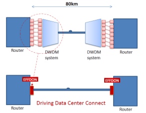 Effdon's CFP does not require the use of external DWDM multiplexing/ demultiplexing and can be added directly onto a router. Source: Effdon Networks
Available 100 Gigabit CFP modules have so far achieved 10km. Now with the Effdon module a 80km reach has been demonstrated that uses 10Gbps optics and no specialist silicon.
Effdon's design is based on the 10x10 MSA (multi-source agreement). "We have managed to resolve the technology barriers - using several techniques - to get to 80km," says Eitan Efron, CEO of Effdon Networks.
There is no 100 Gigabit standard for 80km. The IEEE has two 100 Gigabit standards: the 10km long reach 100GBASE-LR4 and the 40km extended reach 100GBASE-ER4.
Meanwhile, the 100 Gigabit 10x10 MSA based on arrays of 10, 10 Gigabit lasers and detectors, has three defined reaches: 2km, 10km and 40km. At the recent OFC/NFOEC exhibition, Oplink Communication and hybrid integration specialist, Kaiam, showed the 10x10 MSA CFP achieving 40km.
Effdon has not detailed how it has achieved 80km but says its designers have a systems background. "All the software that you need for managing wavelength-division multiplexing (WDM) systems is in our device," says Efron. "Basically we have built a system in a module."
These system elements include component expertise and algorithmic know-how. "Algorithms and software; this is the main IP of the company," says Efron. "We are using 40km components and we are getting 80km."
100 Gigabit landscape
Efron says that while there are alternative designs for 100 Gigabit transmission at 80km or more, each has challenges.
A 100Gbps coherent design achieves far greater reaches but is costly and requires a digital signal processor (DSP) receiver ASIC that consumes tens of watts. No coherent design has yet been implemented using a pluggable module.
Alternative CFP-based 100Gbps direct-detection designs based on a 4x28Gbps architecture exist. But their 28Gbps lanes experience greater dispersion that make achieving 80km a challenge.
MultiPhy's MP1100Q DSP chip counters dispersion. The chip used in a CFP module achieves a 55km point-to-point reach using on-off keying and 800km for dense WDM metro networks using duo-binary modulation.
Finisar and Oclaro also offer 100Gbps direct detection CFP modules for metro dense WDM using duo-binary modulation but without a receiver DSP. ADVA Optical Networking is one system vendor that has adopted such 100Gbps direct-detect modules. Another company developing a 4x28Gbps direct detect module is Oplink Communications.
But Effdon points out that its point-to-point CFP achieves 80km without using an external DWDM multiplexer and demultiplexer - the multiplexing/demultiplexing of the wavelengths is done within the CFP - or external amplification and dispersion compensation. As a result, the CFP plugs straight into IP routers and data centre switches.
"What they [data centre managers] want is what they have today at 10 Gig: ZR [80km] optical transceivers," says Efron

Market demand
"We see a lot of demand for this [80km] solution," says Efron. The design, based on 10 Gigabit optics, has the advantage of using mature high volume components while 25Gbps component technology is newer and available in far lower volumes.
"This [cost reduction associated with volume] will continue; we see 10 Gig lasers going into servers, base stations, data centre switches and next generation PON," says Efron. "Ten Gigabit optical components will remain in higher volume than 25 Gig in the coming years."
The 10x10 MSA CFP design can also be used to aggregate multiple 10 Gig signals in data centre and access networks. This is an emerging application and is not straightforward for the more compact, 4x25Gbps modules as they require a gearbox lane-translation IC.
Reach extension
Effdon Networks' Qbox platform provides data centre managers with 400-800Gbps capacity while offering a reach up to 200km. The box is used with data centre equipment that support CXP or QSFP modules but not the CFP. The 1RU box thus takes interfaces with a reach of several tens of meters to deliver extended transmission.
Qbox supports eight client-side ports - either 40 or 100 Gbps - and four line-facing ports at speeds of 100Gbps or 200Gbps for a reach of 80 to 200km. In future, the platform will deliver 400Gbps line speeds, says Efron.
Samples of the 80km CFP and Qbox are available for selected customers, says Effdon, while general availability of the products will start in the fourth quarter of 2013.

NeoPhotonics' PIC transceiver tackles PON business case
Gazettabyte completes its summary of optical announcements at ECOC, held in Amsterdam. In the third and final part, NeoPhotonics’ GPON multiport transceiver is detailed.
Part 3: NeoPhotonics
 “Anything that can be done to get high utilisation of your equipment, which represents your up-front investment, helps the business case"
Chris Pfistner, NeoPhotonics
NeoPhotonics has announced a Gigabit passive optical network (GPON) transceiver designed to tackle the high up-front costs operators face when deploying optical access.
The GPON optical line terminal (OLT) transceiver has a split ratio of 1:128 - a passive optical network (PON) supporting 128 end points - yet matches the optical link budget associated with smaller split ratios. The transceiver, housed in an extended SFP module, has four fibre outputs, each supporting a conventional GPON OLT. The transceiver also uses a mode-coupling receiver implemented using optical integration.
According to NeoPhotonics, carriers struggle with the business case for PON given the relatively low take-up rates by subscribers, at least initially. “Anything that can be done to get high utilisation of your equipment, which represents your up-front investment, helps the business case,” says Chris Pfistner, vice president of product marketing at NeoPhotonics. “With a device like this, you can now cover four times the area you would normally cover.”
The GPON OLT transceiver, the first of a family, has been tested by operator BT that has described the technology as promising.
Reach and split ratio
The GPON transceiver supports up to 128 end points yet meets the GPON Class B+ 28dB link budget optical transceiver specification.
The optical link budget can be traded to either maximise the PON’s distance, limited due to the loss per fibre-km, or to support higher split ratios. However, a larger split ratio increases the insertion loss due to the extra optical splitter stages the signal passes through. Each 1:2 splitter introduces a 3.5dB loss, eroding the overall optical link budget and hence the PON’s reach.
GPON was specified with a Class B 20dB and Class C 30dB link budget. However once PON deployments started a 28dB Class B+ was created to match the practical requirements of operators. For Verizon, for example, a reach of 10-11km covers 95% of its single family units, says NeoPhotonics.
Operators wanting to increase the split ratio to 1:64 need an extra 4dB. This has led to the 32dB link budget Class C+. For shorter runs, in such cases as China, the Class C+ is used for a 1:128 split ratio. “They [operators] are willing to give up distance to cover an extra 1-by-2 split,” says Pfistner.
NeoPhotonics supports the 1:128 split ratio without suffering such loss by introducing two techniques: the mode-coupling receiver (MCR) and boosting the OLT transceiver's transmitter power.
A key issue dictating a PON performance is the sensitivity of the OLT's burst mode receiver. The upstream fibres are fed straight onto the NeoPhotonics’ MCR, eliminating the need for a 4x1 combiner (inverse splitter) and a resulting 6dB signal loss.
 The GPON OLT transceiver showing the transmit and the mode-coupling receiver. Source: NeoPhotonics
The MCR is not a new concept, says Pfistner, and can be implemented straightforwardly using bulk optics. But such an implementation is relatively large. Instead, NeoPhotonics has implemented the MCR as a photonic integrated circuit (PIC) fitting the design within an extended SFP form factor.
“The PIC draws on our long experience of planar lightwave circuit technology, and [Santur’s] indium phosphide array technology, to do fairly sophisticated devices,” says Pfistner. NeoPhotonics acquired Santur in 2011.
The resulting GPON transceiver module fits within an SFP slot but it is some 1.5-2cm longer than a standard OLT SFP. Most PON line cards support four or eight OLT ports. Pfistner says a 1:4 ratio is the sweet spot for initial rollouts but higher ratios are possible.
On the transmit side, the distributed feedback (DFB) laser also goes through a 1:4 stage which introduces a 6dB loss. The laser transmit power is suitably boosted to counter the 6dB loss.
Operators
BT has trialled the optical performance of a transceiver prototype. “BT confirmed that the four outputs each represents a Class B+ GPON OLT output,” says Pfistner. Some half a dozen operators have expressed an interest in the transceiver, ranging from making a request to working with samples.
China is one market where such a design is less relevant at present. That is because China is encouraging through subsidies the rollout of PON OLTs even if the take-up rate is low. Pfistner, quoting an FTTH Council finding, says that there is a 5% penetration typically per year: “Verizon has been deploying PON for six years and has about a 30% penetration.”
Meanwhile, an operator only beginning PON deployments will first typically go after the neighbourhoods where a high take-up rate is likely and only then will it roll out PON in the remaining areas.
After five years, a 25% uptake is achieved, assuming this 5% uptake a year. At a 4x higher split ratio, that is the same bandwidth per user as a standard OLT in a quarter of the area, says NeoPhotonics.
“One big concern that we hear from operators is: Now I'm sharing the [PON OLT] bandwidth with 4x more users,” says Pfistner. “That is true if you believe you will get to the maximum number of users in a short period, but that is hardly ever the case.”
And although the 1:128 split ratio optical transceiver accounts for a small part of the carrier’s PON costs, the saving the MCR transceiver introduces is at the line card level. "That means at some point you are going to save shelves and racks [of equipment],” says Pfistner.
Roadmap
The next development is to introduce an MCR transceiver that meets the 32dB Class C+ specification. “A lot of carriers are about to make the switch from B+ to C+ in the GPON world,” says Pfistner. There will also be more work to reduce the size of the MCR PIC and hence the size of the overall pluggable form factor.
Beyond that, NeoPhotonics says a greater than 4-port split is possible to change the economics of 10 Gigabit PON, for GPON and Ethernet PON. “There are no deployments right now because the economics are not there,” he adds.
“The standards effort is focussed on the 'Olympic thought': higher bandwidth, faster, further reach, mode-coupling receiver (MCR) whereas the carriers focus is: How do I lower the up-front investment to enter the FTTH market?” says Pfistner.
Further reading:
GPON SFP Transceiver with PIC based Mode-Coupled Receiver, Derek Nesset, David Piehler, Kristan Farrow, Neil Parkin, ECOC Technical Digest 2012 paper.
Lightwave: Mode coupling receiver increases PON split ratios, click here
Ovum: Lowering optical transmission cost at ECOC 2012, click here
Summary Gazettabyte stories from ECOC 2012, click here
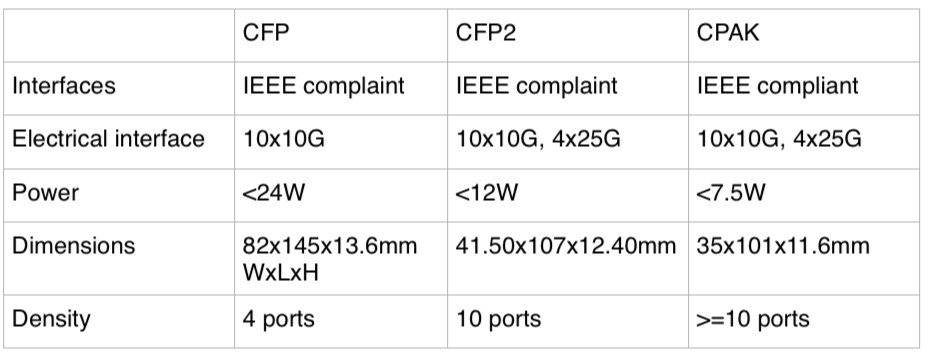
Does Cisco Systems' CPAK module threaten the CFP2?
Cisco Systems has been detailing over recent months its upcoming proprietary optical module dubbed CPAK. The development promises to reduce the market opportunity for the CFP2 multi-source agreement (MSA) and has caused some disquiet in the industry.
Source: Cisco Systems, Gazettabyte, see comments
"The CFP2 has been a bit slow - the MSA has taken longer than people expected - so Cisco announcing CPAK has frightened a few people," says Paul Brooks, director for JDSU's high speed transport test portfolio.
Brooks speculates that the advent of CPAK may even cause some module makers to skip the CFP2 and go straight to the smaller CFP4 given the time lag between the two MSAs is relatively short.
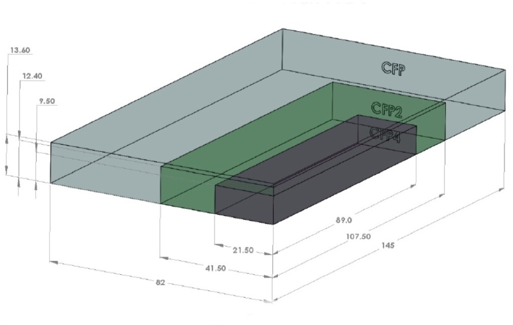
The CPAK module, smaller than the CFP2 MSA and three quarters its volume, has not been officially released and Cisco will not comment on the design but in certain company presentations the CPAK is compared with the CFP. The details are shown in the table above, with the CFP2’s details added.
The CPAK is the first example of Cisco's module design capability following its acquisition of silicon photonics player, Lightwire.
The development of the module highlights how the acquisition of core technology can give an equipment maker the ability to develop proprietary interfaces that promise costs savings and differentiation. But it also raises a question mark regarding the CFP2 and the merit of MSAs when a potential leading customer of the CFP2 chooses to use its own design.
 "The CFP2 has been a bit slow - the MSA has taken longer than people expected - so Cisco announcing CPAK has frightened a few people"
Paul Brooks, JDSU
Industry analysts do not believe it undermines the CFP2 MSA. “I believe there is business for the CFP2,” says Daryl Inniss, practice leader, Ovum Components. “Cisco is shooting for a solution that has some staying power. The CFP2 is too large and the power consumption too high while the CFP4 is too small and will take too long to get to market; CPAK is a great compromise.”
That said, Inniss, in a recent opinion piece entitled: Optical integration challenges component/OEM ecosystem, writes:
“Cisco’s Lightwire acquisition provides another potential attack on the traditional ecosystem. Lightwire provides unique silicon photonics based technology that can support low power consumption and high-density modules. Cisco may adopt a proprietary transceiver strategy to lower cost, decrease time to market, and build competitive barriers. It need not go through the standards process, which would enable its competitors and provide them with its technology. Cisco only needs to convince its customers that it has a robust supply chain and that it can support its product.”
Vladimir Kozlov, CEO of market research firm, LightCounting, is not surprised by the development. “Cisco could use more proprietary parts and technologies to compete with Huawei over the next decade,” he says. “From a transceiver vendor perspective, custom-made products are often more profitable than standard ones; unless Cisco will make everything in house, which is unlikely, it is not bad news.”
JDSU has just announced that its ONT-100G test set supports the CFP2 and CFP4. The equipment will also support CPAK. "We have designed a range of adaptors that allows us to interface to other optics including one very large equipment vendor's - Cisco's - own CFP2-like form factor," says Brooks.
However, Brooks still expects the industry to align on a small number of MSAs despite the advent of CPAK. "The majority view is that the CFP2 and CFP4 will address most people's needs," says Brooks. "Although there is some debate whether a QSFP2 may be more cost effective than the CFP4." The QSFP2 is the next-generation compact follow-on to the QSFP that supports the 4x25Gbps electrical interface.
The CFP2 pluggable module gains industry momentum
Finisar and Oclaro unveiled their first CFP2 optical transceiver products at the recent ECOC exhibition in Amsterdam. JDSU also announced that its ONT-100G test equipment now supports the latest 100Gbps module form factor.
 Source: Oclaro
The CFP2 is the follow-on module to the CFP, supporting the IEEE 100 Gigabit Ethernet and ITU OTU4 standards. It is half the size of the CFP (see image) and typically consumes half the power. Equipment makers can increase the front-panel port density from four to eight by migrating to the CFP2.
Oclaro also announced a second-generation CFP supporting the 100GBASE-LR4 10km and OTU4 standards that reduces the power consumption from 24W to 16W. The power saving is achieved by replacing a two-chip silicon-germanium 'gearbox' IC with a single CMOS chip. The gearbox translates between the 10x10Gbps electrical interface and the 4x25Gbps signals interfacing to the optics.
The CFP2, in contrast, doesn’t include the gearbox IC.
"One of the advantages of the CFP2 module is we have a 4x25Gbps electrical interface," says Rafik Ward, vice president of marketing at Finisar. "That means that within the CFP2 module we can operate without the gearbox chip." The result is a compact, lower-power design, which is further improved by the use of optical integration.
"That 2.5x faster [interface of the CFP2] equates to about a 6x greater difficulty in signal integrity issues, microwave techniques etc"
Paul Brooks, JDSU
The transmission part of the CFP module typically comprises four externally modulated lasers (EMLs), each individually cooled. The four transmitter optical sub-assemblies (TOSAs) then interface to a four-channel optical multiplexer.
Finisar's CFP2 design uses a single TOSA holding four distributed feedback (DFB) lasers, a shared thermo-electric cooler and the multiplexer. The result of using DFBs and an integrated TOSA is that Finisar's CFP2 consumes just 8W.
Oclaro uses photonic integration on the receiver side, integrating four receiver optical sub-assemblies (ROSAs) as well as the optical demultiplexer into a single design, resulting in a 12W CFP2.
At ECOC, Oclaro demonstrated interoperability between its latest CFP and the CFP2. “It shows that the new modules will talk to existing ones,” says Robert Blum, director of product marketing for Oclaro's photonic components.
Meanwhile JDSU demonstrated its ONT-100G test set that supports the CFP2 and CFP4 MSAs.
"Initially the [test set] applications are focused on those doing the fundamental building blocks [for the 100G CFP2] – chip vendors, optical module vendors, printed circuit board developers," says Paul Brooks, director for JDSU's high speed transport test portfolio. "We will roll out more applications within the year that cover early deployment and production."
The standards-based client-side interfaces is an attractive market for test and measurement companies. For line-side optical transmission, much of the development work is proprietary such that developing a test set to serve vendors' proprietary solutions is not feasible.
The biggest engineering challenge for the CFP2 is its adoption of high-speed 25Gbps electrical interfaces. "The CFP was based on third generation, mature 10 Gig I/O [input/output]," says Brooks. "To get to cost-effective CFP2 [modules] is a very big jump: that 2.5x faster [interface] equates to about a 6x greater difficulty in signal integrity issues, microwave techniques etc."
The company says that what has been holding up the emergence of the CFP2 module has been the 104-pin connector: "The pluggable connector is the big headache," says Brooks. "The expectation is that very soon we should get some early connectors."
The test equipment also supports developers of the higher-density CFP4 module, and other form factors such as the QSFP2.
JDSU will start shipping its CFP2 test equipment in the first quarter of 2013.
Oclaro's second-generation CFP and the CFP2 transceivers are sampling, with volume production starting in early 2013.
Finisar's CFP2 LR4 product will sample in 2012 and enter volume production in 2013.