
OIF moves to raise coherent transmission baud rate
"We want the two projects to look at those trade-offs and look at how we could build the particular components that could support higher individual channel rates,” says Karl Gass of Qorvo and the OIF physical and link layer working group vice chair, optical.
 Karl Gass
The OIF members, which include operators, internet content providers, equipment makers, and optical component and chip players, want components that work over a wide bandwidth, says Gass. This will allow the modulator and receiver to be optimised for the new higher baud rate.
“Perhaps I tune it [the modulator] for 40 Gbaud and it works very linearly there, but because of the trade-off I make, it doesn’t work very well anywhere else,” says Gass. “But I’m willing to make the trade-off to get to that speed.” Gass uses 40 Gbaud as an example only, stressing that much work is required before the OIF members choose the next baud rate.
"We want the two projects to look at those trade-offs and look at how we could build the particular components that could support higher individual channel rates”
The modulator and receiver optimisations will also be chosen independent of technology since lithium niobate, indium phosphide and silicon photonics are all used for coherent modulation.
The OIF has not detailed timescales but Gass says projects usually take 18 months to two years.
Meanwhile, the OIF has completed two projects, the specification outputs of which are referred to as implementation agreements (IAs).
One is for integrated dual polarisation micro-intradyne coherent receivers (micro-ICR) for the CFP2. At OFC 2015, several companies detailed first designs for coherent line side optics using the CFP2 module.
The second completed IA is the 4x5-inch second-generation 100 Gig long-haul DWDM transmission module.
UNIC silicon modulator
This is the silicon photonic start-up’s first announced modulator. The design has been developed in conjunction with Sun Microsystems as part of the DAPRA Ultraperformance Nanophotonic Intrachip Communications (UNIC) programme.
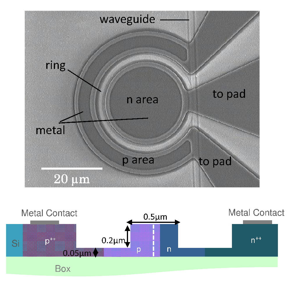 An image of the modulator and a cross-section diagram of the ring waveguide. Source: Kotura
Why is it important?
Optical components use a range of specialist, expensive materials. Silicon is one material that could transform the economics for optics. But for this to happen, the main optical functions – light generation, transmission and detection – need to be supported in silicon. To date, all the required functions except the laser itself - waveguides, modulators and photo-detectors - have been mastered and implemented in silicon.
However, the use of silicon photonics in commercial products has till now been limited. For example, Luxtera makes active optical cable that uses silicon photonics-based transceivers while Kotura has been producing silicon photonics-based VOAs for several years. Its VOA is used within reconfigurable optical add/drop multiplexers (ROADMs) and as a dimmer switch to protect optical receivers from network transients.
Kotura is also supplying its silicon-based Echelle gratings product for 40 and 100 Gigabit Ethernet (GbE) transceiver designs that require the multiplexing and demultiplexing of 4 and 10 wavelengths. The company’s gratings are also being used in Santur’s 100Gbit/s (10x10Gbit/s) transceiver design.
Kotura is in volume production of its VOAs and sampling its Ethernet gratings products, says Arlon Martin, vice-president of marketing and sales at Kotura: “The biggest interest is in 40 Gigabit Ethernet.” Given the small size of the gratings, Kotura is also seeing interest from vendors developing 40GbE transceivers in smaller form factors than the CFP module, such as the QSFP.
This will enable 1Tbit/s data rates over a single fibre to connect high-speed multi-core processor computing elements.
Arlon Martin of Kotura.
But the true potential for silicon photonics, one that promises huge volumes, is very short reach optical interconnects for use in high performance computing and within data centres. Having a low power silicon modulator means it can be integrated with other circuitry in CMOS rather than as a discrete design. Such an integrated approach ensures interconnect reliability.
Method used
There are several ways to modulate a laser. Direct modulation uses electronics to switch the laser on and off at the required rate to imprint the data onto the light. An electro-absorption modulated laser, in contrast, adds an element in front of an always-on laser that either passes or absorbs the light. Kotura’s modulator uses a third approach based on a micro-ring resonator and an adjacent waveguide.
The dimension of the ring – its circumference – dictates when optical resonance occurs. And by carefully matching the power coupling of the micro-ring and waveguide to that of the ring loss, signal attenuation– the light-off condition – is improved. The wavelength at which resonance occurs can be changed by playing with the optical properties of the ring waveguide.
Kotura and Sun have demonstrated the silicon modulator working at up to 11GHz, requiring a peak-to-peak voltage of 2V only. The modulator’s insertion loss is also an attractive 2dB though its working spectrum width is only 0.1nm.
“Our power number – 0.5mW at 10GHz - does not include the driver. But if you want to integrate a number of these on one chip, the low power consumption would enable this,” says Martin. Kotura claims the power consumption achieved is the lowest yet reported.
What next?
The modulator is one of the milestones of the DARPA UNIC programme now into the second of its five-year duration. “This [modulator] is prototype work, not a product,” says Martin, adding that Kotura has not fixed a date as to when the modulator will be commercially used.
As for how the device will ultimately be used, Kotura talks of interfaces operating between 100Gbit/s and 1 Tbit/s. Kotura is already working on an independent programme with CyOptics - the NIST Advanced Technology Programme - developing up to 1Tbit/s links using wavelength division multiplexing (WDM). Such designs use separate laser arrays - each laser at a specific wavelength – as well as gratings and photo-detectors.
In the future inexpensive light sources could generate up to 80 separate modulated lightpaths, Martin says. This will enable 1Tbit/s data rates over a single fibre to connect high-speed multi-core processor computing elements.
Is the idea similar to a broadband light source as proposed for WDM-PON? The UNIC partners have yet to reveal the programme’s detail. “Potentially on the right path,” is all Martin would say.
References:
[1] “Low Vpp, ultralow-energy, compact, high-speed silicon electro-optic modulator.” To read Kotura’s technical paper, click here.
[2] "PHOTONICS APPLIED: INTEGRATED PHOTONICS: Can optical integration solve the computational bottleneck?" OptoIQ, March 1, 2009, click here.