
Lockheed Martin looks to pooling and optical I/O
Electronic systems must peer into ever-greater swathes of the electromagnetic spectrum to ensure a battlefield edge.
Michael HoffSuch electronic systems are used in ground, air, and sea vehicles and even in space.
The designs combine sensors and electronic circuitry for tasks such as radar, electronic warfare, communications and targeting.
Existing systems are custom designs undertaking particular tasks. The challenge facing military equipment makers is that enhancing such systems is becoming prohibitively expensive.
One proposed cost-saving approach is to develop generic radio frequency (RF) and sensor technology that can address multiple tasks.
“Now, each sensor will have to satisfy the requirements for all of the backend processing,” says Michael Hoff, senior research engineer at Lockheed Martin Advanced Technology Laboratories.
Such hardware will be more complex but upgrading systems will become simpler and cheaper. The generic sensors can also be assigned on-the-fly to tackle priority tasks as they arise.
“This is a foundational architectural shift that we see having relevance for many applications,” says Hoff.
Generic sensing
The proposed shift in architectural design was discussed in a paper presented at the IEEE International Symposium on Phased Array Systems and Technology event held in October.
Co-authored by Lockheed Martin and Ayar Labs, the paper focuses on generic sensing and the vast amount of data it generates.
Indeed, the data rates are such that optical interconnect is needed. This is where Ayar Labs comes in with its single-die electro-optical I/O chiplet.
Lockheed Martin splits sensing into two categories: RF sensing and electro-optic/ infrared (or EO/IR). Electro-optic sensors are used for such applications as high-definition imaging.
“When we talk about platform concepts, we typically lump EO/IR into one category,” says Hoff. The EO/IR could be implemented using one broadband sensor or with several sensors, each covering specific wavelengths.
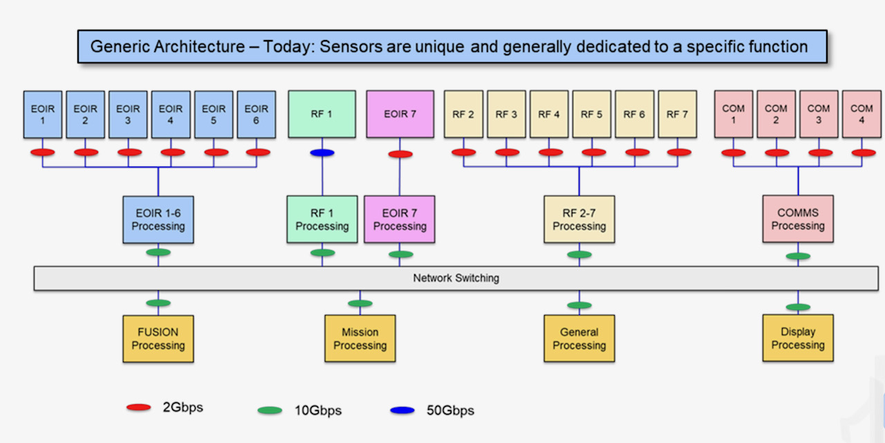
A representation of current systems is shown above. Here, custom designs comprising sensors, analogue circuitry, and processing pass data to mission-processing units. The mission equipment includes data fusion systems and displays.
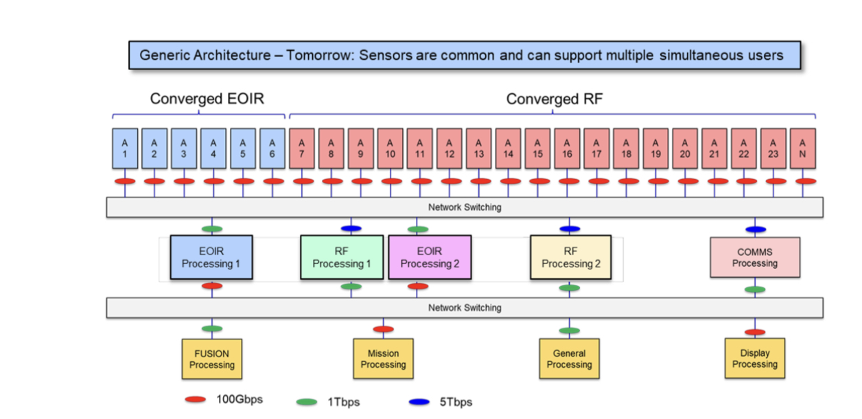
Lockheed Martin proposed architecture uses two generic sensor types – RF and EO/IR – which can be pooled as required (see diagram below).
For example, greater resources may need to be diverted urgently to the radar processing at the expense of communications that can be delayed.
“It’s a more costly individual development, but because it can be shared across different applications and in different teams, cost savings come out ahead,” says Hoff.
An extra networking layer is added to enable the reconfigurability between the sensors and the mission functions and processing systems that use, process, and digest the dat
Optical interconnect
Data traffic generated by modern military platforms continues to rise. One reason is that the frequencies sensed are approaching millimetre-wave. Another is that phased-array systems are using more elements so that more data streams must be be digitised and assessed.
Lockheed Martin cites as an example a military platform comprising 16 phased-array antennas, each with 64 elements.
Each element is sampled with a 14-bit, 100 gigasample-per-second analogue-to-digital converter. The data rate is further doubled since in-phase and quadrature channels are sampled. Each phased array thus generates 179.2 terabits-per-second (Tbps) while the total system data is 2.87 petabits-per-second.
Algorithms at the sensor source can trim the raw data by up to 256x, reducing each antenna’s data stream to 700Gbps, or 11.2Tbps overall.
Optical communications is the only way to transport such vast data flows to the mission processors, says Lockheed Martin.
Multi-chip modules
Any interconnect scheme must not only transfer terabits of data but also be low power and compact.
“The size, weight and power constraints, whether an optical transceiver or processing hardware, get more constrained as you move towards the sensor location,” says Hoff.
The likelihood is that integrated photonics is going to be required as bandwidth demand increases and as the interconnect gets closer to the sensor, he says.
Lockheed Martin proposes using a multi-chip module design that includes the optics, in this case, Ayar Labs’s TeraPhy chiplet.
The TeraPhy combines electrical and silicon photonics circuitry on a single die. Overall, the die has eight transceiver circuits, each supporting eight wavelengths. In turn, each wavelength carries 32 gigabit-per-second (Gbps) of data such that the 54mm2 die transmits 2Tbps in total.
Lockheed Martin has compared its proposed multi-chip module design that includes integrated optics with a discrete solution based on mid-board optics.
The company says integrated optics reduced the power consumed by 5x, from 224W to 45W, while the overall area is reduced a dozen fold, from 3,527 mm2 to 295mm2.
“You’re going to need optical interconnects at many different points,” says Hoff; the exact locations of these multi-chip modules being design-dependent.
Charles Wuischpard, CEO of Ayar Labs, points out that the TeraPhy is built using macro blocks to deliver 2Tbps.
“There are customer opportunities that require far less bandwidth, but what they want is a very tiny chip with very low energy consumption on the input-output [I/O] transport,” says Wuischpard. “There are different areas where the size, weight and power benefits come into play, and it may not all be with our single chiplet solution that we offer.”
Investor
Lockheed Martin became a strategic investor in Ayar Labs in 2019.
“We see this [Ayar Labs’ optical I/O technology] as a foundational technology that we want to be out in front of and want to be first adopters of,” says Hoff.

Data centre photonics - an ECOC report

- ECOC 2022 included talks on optical switching and co-packaged optics.
- Speakers discussed optical switching trends and Google’s revelation that it has been using optical circuit switching in its data centres.
- Nvidia discussed its latest chips, how they are used to build high-performance computing systems, and why optical input-output will play a critical role.
Co-packaged optics and optical switching within the data centre were prominent topics at the recent ECOC 2022 conference and exhibition in Basel, Switzerland.
There were also two notable data centre announcements before ECOC.
Tencent announced it would adopt Broadcom’s Humboldt design, a hybrid co-packaged optics version of the Tomahawk 4 switch chip, in its data centres. Tencent is the first hyperscaler to announce it is adopting co-packaged optics.
Google also revealed its adoption of optical circuit switching in its data centres. Google made the revelation in a paper presented at the Sigcomm 2022 conference held in Amsterdam in August.
Optical circuit switching
Google rarely details its data centre architecture, but when it does, it is usually at Sigcomm.
Google first discussed a decade of evolution of its ‘Jupiter’ data centre architecture in a paper at Sigcomm in 2015.
This year, Google gave an update revealing that it has been using optical circuit switching in its data centres for the past five years. As a result, Google can scale its data centre more efficiently using a reconfigurable optical layer.
Upgrading a data centre’s network is much more complex than upgrading servers and storage. Moreover, a data centre is operational far longer than each generation of equipment. It is thus hard for a data centre operator to foresee how equipment and workloads will evolve over the data centre’s lifetime, says Google.
Google would pre-deploy the spine layer when it started operating a data centre. For Google’s Jupiter architecture, 64 spine blocks, each using 40 gigabit-per-second (Gbps) links, would be deployed. Then, Google added newer aggregation blocks with 100Gbps links. But the hyperscaler could not fully benefit due to the pre-existing 40Gbps spine links.
Google wanted to avoid touching the spine switches. A partial upgrade would have limited benefits, while fully upgrading the spine would take months and be hugely disruptive and costly.
Google’s first solution introduced a MEMS-based optical circuit switching layer between the aggregation and spine blocks.
The MEMS-based switch is data rate agnostic and can support multiple generations of optical modules. The switch’s introduction also allowed Google to add new spine blocks alongside new aggregation blocks; the hyperscaler no longer had to pre-deploy the spine.
At some point, Google decided that for new data centre builds, it would use optical circuit switching only and remove the spine layer of electrical switches.
Adopting optical circuit switch-based interconnect changes Google’s data centres from a clos to a direct-connect architecture. However, not all paths are direct; some take two hops to link aggregation blocks.
Google has developed sophisticated control software to best exploit the direct connectivity for traffic flows.
The software also adapts the network topology – the optical links between the aggregation blocks and their capacities. Such topology changes occur every few weeks, with the system first learning the nature of the traffic and workloads.
Removing the spine layer and replacing it with optical circuit switches has reduced Google’s data centre networking costs by 30 per cent and power consumption by 41 per cent.
ECOC reflections about Google’s optical switch adoption
There was much discussion at ECOC of Google’s use of optical circuit switching in its data centres.
S.J. Ben Yoo, a distinguished professor at the University of California, Davis, gave an ECOC talk about new trends in optical switching. “These are expected future trends,” he said. “I don’t have a crystal ball.”
Prof. Ben Yoo stressed the difficulty of scaling up and scaling out data centre networking architectures in the era of artificial intelligence workloads.
He described co-packaged optics as ‘Trend 0’ because it only delivers bandwidth (input-output capacity).
In contrast, introducing a reconfigurable optical switching layer on top of electrical aggregation switches is the first trend in optical switching. This is what Google has done with its optical circuit switch.
The next development in the data centre, says Ben Yoo, will be the introduction of photonic integrated circuit-based optical switching.
Huawei’s Maxim Kuschnerov, in his ECOC talk, said optical switching in the data centre would only grow in importance.
“Are there use cases where we can use optical switching and what are they?” he said. “I like to take a use-case perspective and find a technology that fulfils that use case.”
His view is that with the classical clos architecture, you can’t just rip out a single layer of electrical switches and replace it with optical ones. “There is a reason why you need all these switches and aggregation functionality,” says Kuschnerov.
Kuschnerov views Google’s optical circuit switching as nothing more than an automated patch panel.
“This is not the optical switch which is the saviour of future data centres,” he says.
Mark Filer, optical network architect, systems and services infrastructure at Google, in an ECOC tutorial detailing how Google uses and benefits from standards, multi-source agreements and open-source developments, was asked about Google’s custom optical switch.

How could Google explain such a custom design if the hyperscaler is such a proponent of open standards? And would Google consider contributing its optical circuit switch and software design to an open community framework?
“My guess is over time, we may see that it finds its way into some kind of open framework,” said Filer, adding that right now, Google sees its optical circuit switch as delivering a competitive advantage.
Co-packaged optics
Benjamin Lee, a senior research scientist at Nvidia, in his ECOC address, discussed the high-performance computing market and the role graphics processing units (GPUs) play in accelerating artificial intelligence and machine learning tasks.
Nvidia not only develops processors, GPUs and data processing unit ICs but also networking silicon and systems that the company uses to make high-performance computing systems.
Lee’s talk addressed the role optical interconnect will play in ensuring continuing scaling of high-performance GPU-based computing systems.
Scaled systems
Nvidia’s latest GPU, announced earlier this year, is the 80-billion-transistor Hopper H100. The H100 deliver a six-fold improvement in throughput compared to Nvidia’s existing A100 GPU announced in 2020.
The Hopper is Nvidia’s first GPU that uses the latest generation of stacked DRAM memory, known as high bandwidth memory 3 (HBM3). In addition, Hopper also uses Nvidia’s fourth-generation NVlink interface.
Eight H100 GPUs fit within Nvidia’s DGX box, as do four Nvidia NVSwitches used to interconnect the GPUs. In addition, an Nvidia Superpod connects 32 DGX nodes – 256 GPUs – using an external tier of NVSwitches.
“A paradigm shift we’re seeing is that switched interconnect is becoming important for scale-up,” said Lee. “So when we want to make the node more computationally powerful, those switches are being put inside the box to connect the GPUs.”
Switch ASIC bandwidths are consistently improving, with 51.2-terabit switch silicon being state-of-the-art. But despite such progress, the scaling is insufficient to keep up with bandwidth requirements, said Lee.
Switch ASIC power consumption is also rising, with advanced CMOS scaling having less impact on designs. Lee foresees switch ASICs consuming 2kW if current trends continue.
In turn, ASIC input-output (I/O) accounts for an increasing portion of the chip’s overall power consumption.
This is true for Nvidia’s GPUs and switch chips, so any I/O technology developed for switching will also benefit its GPUs.
Thus, Nvidia sees optical I/O as the key to scaling the processing performance of its ASICs and computing systems.

I/O metrics
Lee outlined various metrics when discussing optical I/O:
- the electrical interfaces used between the ASIC and optics, and their reach
- the power consumption of the module (the chip, and the chip and optics)
- the system power (of the line card or platform)
- interface density: the capacity exiting a millimetre of surface in terabits-per-second-per-mm (Tbps/mm)
For a system using a 102.4-terabit switch IC, half the power is consumed by the ASIC and half by the edge-board pluggable optics. Here the OIF’s long reach (LR) interface links the two.
The chip’s electrical interfaces consume 4.5 to 6.5 picojoule-per-bit (pJ/b) such that the total switch IC I/O power consumed is 450W.
The next step is co-packaged optics. Here, optical chiplets are placed closer to the ASIC (100mm away) such that the OIF’s lower power XSR (extra short reach) interface can be used that consumes 1.24-1.7pJ/s, says Lee.
Again taking a module view, Nvidia views the co-packaged design as comprising two electrical interfaces (the XSR interface between the chip and optical chiplets either side) and one optical interface.
This equates to 250W per chip module, a modest power saving at the chip module level but a significant power saving at the system level, given the optics is now part of the module.
However, bandwidth density is 475-870Gbps/mm, and for beyond 100-terabit switches, a further fourfold improvement is needed: 2Tbps/mm and, ultimately, 10Tbps/mm.
Just achieving a 2Tb/s/mm interface density will be challenging, says Lee.
For that, 2.5D co-packaged optics will be needed with the ASIC and chiplets sharing a silicon interposer that enables higher wire densities.
2.5D integration is already an established technology in the semiconductor industry; Nvidia has been using the technology for its GPUs since 2016.
The technology enables much closer coupling between the ASIC and optics (some 1mm), resulting in sub 1pJ/bit. Nvidia cites research showing a 0.3pJ/b has already been achieved.
Scaling I/O
Lee outlined all the ways I/O can be scaled.
Baud rate is one approach, but the energy efficiency diminishes as the symbol rate increases, from 50 to 100 to 200 gigabaud.
Modulation is another approach, moving from non-return-to-zero to 4-level pulse amplitude modulation (PAM-4) and even higher PAM schemes. The challenge is that the signal-to-noise ratio diminishes the higher the PAM scheme, requiring additional digital signal processing which, in turn, consumes more power.
Another technique, polarization, can be used to double the data rate. Then there is the spatial domain. Here, tighter pitches can be used, says Lee, moving from 250, 127 and even 80 microns before other approaches are needed. These include multi-core fibre, waveguide fan-outs and even bidirectional optics (what Google uses for its optical circuit switch ports, to save on fibre and port count).
All these spatial approaches require considerable development and operational costs, says Lee.
The most promising way to boost throughput and increase interface density is using wavelength division multiplexing (WDM).
Nvidia has produced several generations of test chips that use wavelength parallelism in the O-band based on micro-ring resonators.
Nvidia’s steer
Micro-ring resonator technology already supports 100Gbps modulation rates. The optical circuit is also compact, energy-efficient and supports wavelength scaling.
Lee also outlined other key technologies that will be needed, each bringing their own challenges. One is the external laser source, another is advanced packaging.
Nvidia believes that for future generations of ASICs, dense WDM mirror-ring modulated links offer the most promising approach to meeting both low power and the massive interface density improvements that will be needed.
This will require low-cost lasers while packaging remains a severe challenge.
2.5D integration is going to be an important step in the evolution of switch interconnect, concluded Lee.

OpenLight's integrated-laser silicon photonics platform

- OpenLight is an independent silicon photonics company backed by Synopsys and Juniper Networks
- The company was created by carving out the silicon photonics arm of Juniper
- The establishment of OpenLight and its open platform highlights the growing maturity of silicon photonics as new applications emerge beyond datacom and telecom
OpenLight is coming to market with an open silicon photonics platform that includes integrated lasers and gain blocks.
Juniper has a long relationship with Synopsys, using its electronic-photonic design automation (EPDA) tools.
So when Juniper said it was spinning out its silicon photonics group, Synopsys was keen to partner. The result is OpenLight, of which Synopsys has a 75 per cent stake costing $67.5 million.
Thomas Mader, OpenLight’s chief operating officer and formerly head of Juniper’s silicon photonics unit, says OpenLight is the first company to offer an open platform that includes monolithically integrated lasers, optical amplifiers and modulators.
Juniper Networks and Synopsys
Juniper gained its silicon photonics technology in 2016 when it acquired Aurrion for $165 million.
Aurrion was a fabless silicon photonics start-up from the University of California, Santa Barbara, with a heterogeneous integration silicon photonics process that includes III-V materials, enabling integrated lasers as part of a photonic circuit.
OpenLight is now making this technology available through its partnership with the foundry Tower Semiconductor.
Juniper’s interests are mainly datacom and telecom, but it recognises the emerging opportunities for silicon photonics such as Lidar, optical computing, high-performance computing and optical interconnect.
“With this kind of technology, you want to drive volumes,” says Mader.

Juniper saw spinning out the unit and opening up access to the technology as the best way to drive volumes and reduce costs. The arrangement also benefits Juniper’s own technology needs.
Synopsys, meanwhile, believes it is the right time to back the OpenLight venture.
“We think it [the open platform] is a great opportunity for growth for Synopsys’s EPDA tools,” says John Koeter, senior vice president of marketing and strategy, solutions group at Synopsys.
OpenLight will give Synopsys insight into how the market is evolving and benefit the company’s tools and, eventually, its IP.
Business model
OpenLight is licensing its process design kit (PDK), the files that model Tower’s fabrication process. A company can enter into an agreement with Tower, access the PDK and design its silicon photonics device.
“What we are offering through Tower, and what we spent significant effort developing and showing Tower how to do, is monolithically integrating lasers and optical gain,” says Mader. “Tower is the first time we’re on a volume eight-inch [wafer] process.”
Juniper entered into a partnership with Tower Semiconductor in 2019.
“We are doing the first MPW [multi-project wafer] this summer with Tower on this process,” says Mader.
OpenLight is also providing designs it has developed and validated for several customers. “But we are not selling PICs [photonic integrated circuits]; that is not part of our plan,” says Mader.
OpenLight intends to partner with other foundries to make more widely available integrated-laser designs.

For now, though, OpenLight is focussed on ratifying its roadmap for the next two years.
“We’re going to be busy building out the component library for Tower to keep customers interested because better components make better circuits,” says Daniel Sparacin, vice president of business development and strategy at OpenLight.
OpenLight offers a 100-gigabit modulator and is working on its next-generation 200-gigabit modulator.
“We’re mostly O-band right now, and we have C-band coming up in the roadmap very shortly,” says Sparacin.
Applications
OpenLight has 400 and 800-gigabit optical designs for the data centre to help customers bring to market their PIC developments.
The company is also seeing interest from Lidar customers, particularly those pursuing coherent-based designs.
“The main reason is the integrated laser,” says Mader. “Otherwise, with standard silicon photonics, you have to attach a laser separately, which doesn’t scale well to multiple channels.” That’s because attaching multiple lasers impacts yield.
Lidar also benefits from on-chip optical amplification. “When you have a complex chip, you have a lot of losses,” says Mader.
OpenLight is working with firms pursuing optical computing for machine learning which promises greater power efficiency. “There are several of them coming to us because we can put hundreds or thousands of indium phosphide elements monolithically on a chip,” says Mader.
OpenLight says it has no position regarding co-packaged optics and whether a design uses an external light source or integrated lasers.
It believes co-packaged optics designs will eventually use integrated light sources, but its technology supports both and can even be used to make external light sources.
Overall, OpenLight says it is working with dozens of companies.
Design tools and integration
Synopsys has been an early mover with its integrated optical design automation tools. The tools include:
- OptoCompiler, a photonic IC design environment.
- The OptSim photonic circuit and system simulator.
- The Sentaurus TCAD and RSoft Photonic Device tools for process modelling and device design.
Working closely with OpenLight will benefit Synopsys’s tool environment, says Koeter. Synopsys is adding functionalities and design capabilities to its tools to support the integration of lasers. OpenLight is also providing Synopsys feedback on what will improve the experience of using its design platform.
Synopsys is one of three leading electronic design automation (EDA) tool companies. However, design tools for photonics are a more recent development.
“EDA quite a while ago is where photonic design is now going,” says Mader.
Integration is the underlying trend driving optics.
“We see the scaling already with 400- and 800-gigabit for datacom and some of the other applications; you see the shift to silicon photonics,” says Mader. “The higher the complexity, the more you see it shifting this way because there’s a cost advantage with the integrated laser and optical gain.”
Photonics may not come close to chip designs with billions of transistors. Still, photonic designs that go beyond four-channel design to ones with 32 or 64 channels or optical computing with hundreds or thousands of components are emerging.
“So you see a scaling even though it’s decades behind the electronics field,” says Mader.
With monolithically integrated lasers, yields remain high, whereas scaling a design with discrete components results in unacceptable yields.
“And so we will be able to go where you can’t go otherwise,” says Mader. “It’s not billions, but even dozens [of components] at this point is revolutionary.”
Intel adds multi-channel lasers to its silicon photonics toolbox

Intel has developed an 8-lane parallel-wavelength laser array to tackle the growing challenge of feeding data to integrated circuits (ICs).
Optical input-output (I/O) promises to solve the challenge of getting data into and out of high-end silicon devices.
These ICs include Ethernet switch chips and ‘XPUs’, shorthand for processors (CPUs), graphics processing units (GPUs) and data processor units (DPUs).
The laser array is Intel’s latest addition to its library of silicon photonics devices.
Power wall
A key challenge facing high-end chip design is the looming ‘power wall’. The electrical I/O power consumption of advanced ICs is rising faster than the power the chip consumes processing data.
James Jaussi, senior principal engineer and director, PHY research lab at Intel Labs, says if this trend continues, all the chip’s power will be used for communications and none will be left for processing, what is known as the power wall.
One way to arrest this trend is to use optical rather than electrical I/O by placing chiplets around the device to send and receive data optically.
Using optical I/O simplifies the electrical I/O needed since the chip only sends data a short distance to the adjacent chiplets. Once in the optical domain, the chiplet can send data at terabit-per-second (Tbps) speeds over tens of meters.
However, packaging optics with a chip is a significant design challenge and changes how computing and switching systems are designed and operated.

Laser array
Intel has been developing silicon photonics technology for two decades. The library of devices includes ring-resonators used for modulation and detection, photo-detectors, lasers, and semiconductor optical amplifiers.

Intel can integrate lasers and gain blocks given its manufacturing process allows for the bonding of III-V materials to a 300mm silicon wafer, what is known as heterogeneous integration.
The company has already shipped over 6 million silicon photonics-based optical modules – mainly its 100-gigabit PSM-4 and 100-gigabit CWDM-4 – since 2016.
Intel also ships such modules as the 100G LR4, 100G DR/FR, 200G FR4, 400G DR4 and 400G FR4. The company says it makes two million optical modules a year.
Now Intel Labs has demonstrated a laser array that integrates eight distributed feedback (DFB) lasers for wavelength-division multiplexing (WDM) transmissions. In addition, the laser array is compliant with the CW-WDM multi-source agreement.
“This is a much more difficult design,” says Haisheng Rong, senior principal engineer, photonics research at Intel Labs. “The challenge here is that you have a very small channel spacing of 200GHz.”
Each laser’s wavelength is defined by the structure of the silicon waveguide – less than 1 micron wide and tens of microns long – and the periodicity of a Bragg reflector grating.
The lasers in the array are almost identical, says Rong, their difference being defined by the Bragg grating’s period. There is a 0.2nm difference in the grating period of adjacent – 200GHz apart – lasers. For 100GHz spacing, the grating period difference will need to be 0.1nm.
Specifications
The resulting eight wavelengths have uniform separation. Intel says each wavelength is 200GHz apart with a tolerance of plus or minus 13GHz, while the lasers’ output power varies by plus or minus 0.25dB.
Such performance is well inside the CW-WDM MSA specifications that call for a plus or minus 50GHz tolerance for 200GHz channel spacings and plus or minus 1dB variability in output power.
Rong says that using a 200GHz channel enables a baud rate of 64 gigabaud (GBd) or 128GBd. Intel has already demonstrated its electronic and photonic ICs (EIC/ PIC) operating at 50 gigabit-per-second (Gbps) and 112Gbps.
In future, higher wavelength counts – 16- and 32-channel designs – will be possible, as specified by the CW-WDM MSA.
The laser array’s wavelengths vary with temperature and bias current. For example, the laser array operates at 80oC, but Intel says it can work at 100oC.
Products
The working laser array is the work of Intel Labs, not Intel’s Silicon Photonics Products Division. Intel has yet to say when the laser array will be adopted in products.
But Intel says the technology will enable terabit-per-second (Tbps) transmissions over fibre and reach tens of meters. The laser array also promises 4x greater I/O density and energy efficiency of 0.25 picojoules-per-bit (pJ/b), two-thirds that of the PCI Express 6.0 standard.
Another benefit of optical I/O is low latency, under 10ns plus the signal’s time of flight, determined by the speed of light in the fibre and the fibre’s length.
An electrical IC is needed alongside the optical chiplet to drive the optics and control the ring-resonator modulators and lasers. The chip uses a 28nm CMOS process and Intel is investigating using a 22nm process.
Optical I/O goals
Intel announced in December 2021 that it was working with seven universities as part of its Integrated Photonics Research Center.
The goal is to create building-block circuits that will meet optical I/O needs for the next decade-plus, says Jaussi.
Intel aims to demonstrate by 2024 sending 4Tbps over a fibre while consuming 0.25pJ/b.
Intel sets a course for scalable optical input-output

- Intel is working with several universities to create building-block circuits to address its optical input-output (I/O) needs for the next decade-plus.
- By 2024 the company wants to demonstrate the technologies achieving 4 terabits-per-second (Tbps) over a fibre at 0.25 picojoules-per-bit (pJ/b).
Intel has teamed up with seven universities to address the optical I/0 needs for several generations of upcoming products.
The initiative, dubbed the Intel Research Center for Integrated Photonics for Data Centre Interconnects, began six months ago and is a three-year project.
No new location is involved, rather the research centre is virtual with Intel funding the research. By setting up the centre, Intel’s goal is to foster collaboration between the research groups.
Motivation
James Jaussi, senior principal engineer and director of the PHY Research Lab in Intel Labs, (pictured) heads a research team that focuses on chip-to-chip communication involving electrical and optical interfaces.
“My team is primarily focussed on optical communications, taking that technology and bringing it close to high-value silicon,” says Jaussi.
Much of Jaussi’s 20 years at Intel has focussed on electrical I/O. During that time, the end of electrical interfaces has repeatedly been predicted. But copper’s demise has proved overly pessimistic, he says, given the advances made in packaging and printed circuit board (PCB) materials.
But now the limits of copper’s bandwidth and reach are evident and Intel’s research arm wants to ensure that when the transition to optical occurs, the technology has longevity.
“This initiative intends to prolong the [optical I/O] technology so that it has multiple generations of scalability,” says Jaussi. And by a generation, Jaussi means the 3-4 years it takes typically to double the bandwidth of an I/O specification.
Co-packaged optics and optical I/O
Jaussi distinguishes between co-packaged optics and optical I/O.
He describes co-packaged optics as surrounding a switch chip with optics. Given the importance of switch chips in the data centre, it is key to maintain compatibility with specifications, primarily Ethernet.
But that impacts the power consumption of co-packaged optics. “The power envelope you are going to target for co-packaged optics is not necessarily going to meet the needs of what we refer to as optical I/O,” says Jaussi.
Optical I/O involves bringing the optics closer to ICs such as CPUs and graphics processor units (GPUs). Here, the optical I/O need not be aligned with standards.
The aim is to take the core I/O off a CPU or GPU and replace it with optical I/O, says Jaussi.
With optical I/O, non-return-to-zero (NRZ) signalling can be used rather than 4-level pulse amplitude modulation (PAM-4). The data rates are slower using NRZ but multiple optical wavelengths can be used in parallel. “You can power-optimise more efficiently,” says Jaussi.
Ultimately, co-packaged optics and optical I/O will become “stitched together” in some way, he says.
Research directions
One of the research projects involves the work of Professor John Bowers and his team at the University of California, Santa Barbara, on the heterogeneous integration of next-generation lasers based on quantum-dot technology.
Intel’s silicon photonics transceiver products use hybrid silicon quantum well lasers from an earlier collaboration with Professor Bowers.
The research centre work is to enable scalability by using multi-wavelength designs as well as enhancing the laser’s temperature performance to above 100oC. This greater resilience to temperature helps the laser’s integration alongside high-performance silicon.
Another project, that of Professor Arka Majumdar at the University of Washington, is to develop non-volatile reconfigurable optical switching using silicon photonics.
“We view this as a core building block, a capability,” says Jaussi. The switching element will have a low optical loss and will require liitle energy for its control.
The switch being developed is not meant to be a system but an elemental building block, analogous to a transistor, Intel says, with the research exploring the materials needed to make such a device.
The work of Professor S.J. Ben Yoo at University of California, Davis, is another of the projects.
His team is developing a silicon photonics-based modulator and a photodetector technology to enable 40-terabit transceivers at 150fJ/bit and achieving 16Tb/s/mm I/O density.
“The intent is to show over a few fibres a massive amount of bandwidth,” says Jaussi.
Goals
Intel says each research group has its own research targets that will be tracked.
All the device developments will be needed to enable the building of something far more sophisticated in future, says Jaussi.
At Intel Labs’ day last year, the company spoke about achieving 1Tbps of I/O at 1pJ/s. The research centre’s goals are more ambitious: 4Tbps over a fibre at 0.25pJ/b in the coming three years.
There will be prototype demonstrations showing data transmissions over a fibre or even several fibres. “This will allow us to make that scalable not just for one but two, four, 10, 20, 100 fibres,” he says. “That is where that parallel scalability will come from.”
Intel says it will be years before this technology is used for products but the research goals are aggressive and will set the company’s optical I/O goals.

Turning to optical I/O to open up computing pinch points

Getting data in and out of chips used for modern computing has become a key challenge for designers.
A chip may talk to a neighbouring device in the same platform or to a chip across the data centre.
The sheer quantity of data and the reaches involved – tens or hundreds of meters – is why the industry is turning to optical for a chip’s input-output (I/O).
It is this technology transition that excites Ayar Labs.
The US start-up showcased its latest TeraPHY optical I/O chiplet operating at 1 terabit-per-second (Tbps) during the OFC virtual conference and exhibition held in June.
Evolutionary and revolutionary change
Ayar Labs says two developments are driving optical I/O.
One is the exponential growth in the capacity of Ethernet switch chips used in the data centre. The emergence of 25.6-terabit and soon 51.2-terabit Ethernet switches continue to drive technologies and standards.
This, says Hugo Saleh, vice president of business development and marketing, and recently appointed as the managing director of Ayar Labs’ new UK subsidiary, is an example of evolutionary change.
But artificial intelligence (AI) and high-performance computing have networking needs independent of the Ethernet specification.
“Ethernet is here to stay,” says Saleh. “But we think there is a new class of communications that is required to drive these advanced applications that need low latency and low power.”
Manufacturing processes
Ayar Labs’ TeraPHY chiplet is manufactured using GlobalFoundries’ 45nm RF Silicon on Insulator (45RFSOI) process. But Ayar Labs is also developing TeraPHY silicon using GlobalFoundries’ emerging 45nm CMOS-silicon photonics CLO process (45CLO).
The 45RFSOI process is being used because Ayar Labs is already supplying TeraPHY devices to customers. “They have been going out quite some time,” says Saleh.
But the start-up’s volume production of its chiplets will use GlobalFoundries’ 45CLO silicon photonics process. Version 1.0 of the process design kit (PDK) is expected in early 2022, leading to qualified TeraPHY parts based on the process.
One notable difference between the two processes is that 45RFSOI uses a vertical grating coupler to connect the fibre to the chiplet which requires active alignment. The 45CLO process uses a v-groove structure such that passive alignment can be used, simplifying and speeding up the fibre attachment.
“With high-volume manufacturing – millions and even tens of millions of parts – things like time-in-factory make a big difference,” says Saleh. Every second spent adds cost such that the faster the processes, the more cost-effective and scalable the manufacturing becomes.
Terabit TeraPHY
The TeraPHY chiplet demonstrated during OFC uses eight optical transceivers. Each transceiver comprises eight wavelength-division multiplexed (WDM) channels, each supporting 16 gigabit-per-second (Gbps) of data. The result is a total optical I/O bandwidth of 1.024Tbps operating in each direction (duplex link).
“The demonstration is at 16Gbps and we are going to be driving up to 25Gbps and 32Gbps next,” says Saleh.
The chiplet’s electrical I/O is slower and wider: 16 interfaces, each with 80, 2Gbps channels implementing Intel’s Advanced Interface Bus (AIB) technology.
Last December, Ayar Labs showcased advanced parts using the CLO process. The design was a direct-drive part – a prototype of a future-generation product, not the one demonstrated for OFC.
“The direct-drive part has a serial analogue interface that could come from the host ASIC directly into the ring resonators and modulate them whereas the part we have today is the productised version of an AIB interface with all the macros and all the bandwidth enabled,” says Saleh.
Ayar Labs also demonstrated its 8-laser light source, dubbed SuperNova, that drives the chiplet’s optics.
The eight distributed feedback (DFB) lasers are mixed using a planar lightwave circuit to produce eight channels, each comprising eight frequencies of light.
Saleh compares the SuperNova to a centralised power supply in a server that power pools of CPUs and memory. “The SuperNova mimics that,” he says. “One SuperNova or a 1 rack-unit box of 16 SuperNovas distributing continuous-wave light just like distributed voltage [in a server].”
The current 64-channel SuperNova powers a single TeraPHY but future versions will be able to supply light to two or more.
Ayar Labs is using Macom as its volume supplier of DFB lasers.
Significance
Ayar Labs believes the 1-terabit chip-to-chip WDM link is an industry first.
The demo also highlights how the company is getting closer to a design that can be run in the field. The silicon was made less than a month before the demonstration and was assembled quickly. “It was not behind glass and was operating at room temperature,” says Saleh. “It’s not a lab setting but a production setting.”
The same applies to the SuperNova. The light source is compliant with the Continuous-Wave Wavelength Division Multiplexing (CW-WDM) Multi-Source Agreement (MSA) Group that released its first specification revision to coincide with OFC. The CW-WDM MSA Group has developed a specification for 8, 16, and 32-wavelength optical sources.
The CW-WDM MSA promoter and observer members include all the key laser makers as well as the leading ASIC vendors. “We hope to establish an ecosystem on the laser side but also on the optics,” says Saleh.
“Fundamentally, there is a change at the physical (PHY) level that is required to open up these bottlenecks,” says Saleh. “The CW-WDM MSA is key to doing that; without the MSA you will not get that standardisation.”
Saleh also points to the TeraPHY’s optical I/O’s low power consumption which for each link equates to 5pJ/bit. This is about a tenth of the power consumed by electrical I/O especially when retimers are used. Equally, the reach is up to 2km not tens of centimetres associated with electrical links.
Chiplet demand
At OFC, Arista Networks outlined how pluggable optics will be able to address 102.4 terabit Ethernet switches while Microsoft said it expects to deploy co-packaged optics by the second half of 2024.
Nvidia also discussed how it clusters its graphics processing units (GPUs) that are used for AI applications. However, when a GPU from one cluster needs to talk to a GPU in another cluster, a performance hit occurs.
Nvidia is looking for the optical industry to develop interfaces that will enable its GPU systems to scale while appearing as one tightly coupled cluster. This will require low latency links. Instead of microseconds and milliseconds depending on the number of hops, optical I/O reduces the latency to tens of nanoseconds.
“We spec our chiplet as sub-5ns plus the time of flight which is about 5ns per meter,” says Saleh. Accordingly, the transit time between two GPUs 1m apart is 15ns.
Ayar Labs says that after many conversations with switch vendors and cloud players, the consensus is that Ethernet switches will have to adopt co-packaged optics. There will be different introductory points for the technology but the industry direction is clear.
“You are going to see co-packaged optics for Ethernet by 2024 but you should see the first AI fabric system with co-packaged I/O in 2022,” says Saleh.
Intel published a paper at OFC involving its Stratix 10 FPGA using five Ayar Labs’ chiplets, each one operating at 1.6 terabits (each optical channel operating at 25Gbps, not 16Gbps). The resulting FPGA has an optical I/O capacity of 8Tbps, the design part of the US DARPA PIPES (Photonics in the Package for Extreme Scalability) project.
“A key point of the paper is that Intel is yielding functional units,” says Saleh. The paper also highlighted the packaging and assembly achievements and the custom cooling used.
Intel Capital is a strategic investor in Ayar Labs, as is GlobalFoundries, Lockheed Martin Ventures, and Applied Materials.