
Drut's agile optical fabric for the data centre
A US start-up has developed a photonic fabric for the data centre that pulls together the hardware needed for a computational task.
Drut Technologies offers management software and a custom line card, which, when coupled with the optical switch, grabs the hardware required for the workload.
“You can have a server with lots of resource machines: lots of graphic processing units (GPUs) and lots of memory,” says Bill Koss, CEO of Drut. “You create a machine, attach a workload to it and run it; forever, for a day, or 15 minutes.”
Drut first showcased its technology supporting the PCI Express (PCIe) bus over photonics at server specialist, SuperMicro’s exhibition stand, at the Supercomputing 22 show held last November in Dallas, Texas.
“This is a fully reconfigurable, direct-connect optical fabric for the data centre,” says Koss.
Drut says hyperscalers use between 40 and 60 per cent of the hardware in their data centres. With direct connectivity, resources can be used as needed and released, improving overall hardware utilisation.
Optical circuit switching
Drut’s system is a second recent example of a company using optics for the data centre to establish reconfigurable photonic paths between endpoints, referred to as optical circuit switching.
Google revealed in August 2022 that it had developed its own MEMS-based optical switch design, which the hyperscaler has used for several years in its data centres.
The optical circuit switches are used instead of the highest tier of Ethernet switches – the spine layer – in Google’s data centres.
Using optical circuit switching reduces networking costs by 30 per cent and power consumption by over 40 per cent. The optical switch layer also enables more efficient and less disruptive upgrading of the server endpoints.
Koss says the difference between its design and Google’s is scale: “Ours is more granular.”
Drut says its solution will enable racks of optically-attached machines, but unlike Google, the optical switching is much closer to the end equipment. Indeed, it is a second fabric independent of the data centre’s tiered Ethernet switches.

Product architecture
The main three elements of Drut’s technology are an FPGA-based line card, the fabric-manager software and a third-party optical switch.
Drut’s line card, the iFIC 1000, has an FPGA and four 100-gigabit transceivers. “That is as much as we can fit on,” says Koss.

The company uses its own transport protocol that runs over the fabric, an ‘out-of-band’ network design.
“You can dynamically attach and detach, and the machine doesn’t go into crazy land,” says Koss.
The fabric manager knows all the ports of the switch and the endpoints and sets up the desired system configurations.
With the fabric management software and the FPGA, the system can configure banks of graphic processing units (GPUs).
Drut has also demonstrated linking memory over its photonic fabric, although this is in development and still unavailable as a product.
Drut says a primary challenge was developing the FPGA that takes the out-of-band signalling off the main bus and supports it over the optical fabric.
A photonic fabric design promises to change the nature of a server. A user will request CPUs, accelerators such as GPUs and FPGAs, and memory, as needed, for each workload.
The merits of using an optical switch include its support for multiple ports, i.e. the switch’s large radix, and its being interface-speed agnostic.
The photonic switch also has a lower latency than switch ICs and simplifies cabling. “It is all single-mode fibre pluggable optics,” says Koss.

Status
Drut is developing a second line card which will use a larger FPGA. Each card generation will expand the number of optical ports to scale the endpoints supported.
The company is also working with a co-packaged optics player on a design for a hyperscaler.
“We use pluggable optics today because co-packaged optics isn’t available,” says Koss.
The advantage of co-packaged optics is that it will increase the port density on each line card and hence the overall scaling.
Koss says that Drut already has two customers: an enterprise and a cloud provider.
Drut, which means ‘high tempo’ in Sanskrit, has so far secured two rounds of funding.
“We did a good-sized seed round in June 2021 and closed a bigger seed extension last September; not an easy task in 2022,” says Koss. “We added Boston Seed Capital and another firm as new investors as well.”
The company has sufficient funding till 2024 and is talking to new investors for a Series A funding round.

Data centre photonics - an ECOC report

- ECOC 2022 included talks on optical switching and co-packaged optics.
- Speakers discussed optical switching trends and Google’s revelation that it has been using optical circuit switching in its data centres.
- Nvidia discussed its latest chips, how they are used to build high-performance computing systems, and why optical input-output will play a critical role.
Co-packaged optics and optical switching within the data centre were prominent topics at the recent ECOC 2022 conference and exhibition in Basel, Switzerland.
There were also two notable data centre announcements before ECOC.
Tencent announced it would adopt Broadcom’s Humboldt design, a hybrid co-packaged optics version of the Tomahawk 4 switch chip, in its data centres. Tencent is the first hyperscaler to announce it is adopting co-packaged optics.
Google also revealed its adoption of optical circuit switching in its data centres. Google made the revelation in a paper presented at the Sigcomm 2022 conference held in Amsterdam in August.
Optical circuit switching
Google rarely details its data centre architecture, but when it does, it is usually at Sigcomm.
Google first discussed a decade of evolution of its ‘Jupiter’ data centre architecture in a paper at Sigcomm in 2015.
This year, Google gave an update revealing that it has been using optical circuit switching in its data centres for the past five years. As a result, Google can scale its data centre more efficiently using a reconfigurable optical layer.
Upgrading a data centre’s network is much more complex than upgrading servers and storage. Moreover, a data centre is operational far longer than each generation of equipment. It is thus hard for a data centre operator to foresee how equipment and workloads will evolve over the data centre’s lifetime, says Google.
Google would pre-deploy the spine layer when it started operating a data centre. For Google’s Jupiter architecture, 64 spine blocks, each using 40 gigabit-per-second (Gbps) links, would be deployed. Then, Google added newer aggregation blocks with 100Gbps links. But the hyperscaler could not fully benefit due to the pre-existing 40Gbps spine links.
Google wanted to avoid touching the spine switches. A partial upgrade would have limited benefits, while fully upgrading the spine would take months and be hugely disruptive and costly.
Google’s first solution introduced a MEMS-based optical circuit switching layer between the aggregation and spine blocks.
The MEMS-based switch is data rate agnostic and can support multiple generations of optical modules. The switch’s introduction also allowed Google to add new spine blocks alongside new aggregation blocks; the hyperscaler no longer had to pre-deploy the spine.
At some point, Google decided that for new data centre builds, it would use optical circuit switching only and remove the spine layer of electrical switches.
Adopting optical circuit switch-based interconnect changes Google’s data centres from a clos to a direct-connect architecture. However, not all paths are direct; some take two hops to link aggregation blocks.
Google has developed sophisticated control software to best exploit the direct connectivity for traffic flows.
The software also adapts the network topology – the optical links between the aggregation blocks and their capacities. Such topology changes occur every few weeks, with the system first learning the nature of the traffic and workloads.
Removing the spine layer and replacing it with optical circuit switches has reduced Google’s data centre networking costs by 30 per cent and power consumption by 41 per cent.
ECOC reflections about Google’s optical switch adoption
There was much discussion at ECOC of Google’s use of optical circuit switching in its data centres.
S.J. Ben Yoo, a distinguished professor at the University of California, Davis, gave an ECOC talk about new trends in optical switching. “These are expected future trends,” he said. “I don’t have a crystal ball.”
Prof. Ben Yoo stressed the difficulty of scaling up and scaling out data centre networking architectures in the era of artificial intelligence workloads.
He described co-packaged optics as ‘Trend 0’ because it only delivers bandwidth (input-output capacity).
In contrast, introducing a reconfigurable optical switching layer on top of electrical aggregation switches is the first trend in optical switching. This is what Google has done with its optical circuit switch.
The next development in the data centre, says Ben Yoo, will be the introduction of photonic integrated circuit-based optical switching.
Huawei’s Maxim Kuschnerov, in his ECOC talk, said optical switching in the data centre would only grow in importance.
“Are there use cases where we can use optical switching and what are they?” he said. “I like to take a use-case perspective and find a technology that fulfils that use case.”
His view is that with the classical clos architecture, you can’t just rip out a single layer of electrical switches and replace it with optical ones. “There is a reason why you need all these switches and aggregation functionality,” says Kuschnerov.
Kuschnerov views Google’s optical circuit switching as nothing more than an automated patch panel.
“This is not the optical switch which is the saviour of future data centres,” he says.
Mark Filer, optical network architect, systems and services infrastructure at Google, in an ECOC tutorial detailing how Google uses and benefits from standards, multi-source agreements and open-source developments, was asked about Google’s custom optical switch.

How could Google explain such a custom design if the hyperscaler is such a proponent of open standards? And would Google consider contributing its optical circuit switch and software design to an open community framework?
“My guess is over time, we may see that it finds its way into some kind of open framework,” said Filer, adding that right now, Google sees its optical circuit switch as delivering a competitive advantage.
Co-packaged optics
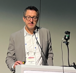
Benjamin Lee, a senior research scientist at Nvidia, in his ECOC address, discussed the high-performance computing market and the role graphics processing units (GPUs) play in accelerating artificial intelligence and machine learning tasks.
Nvidia not only develops processors, GPUs and data processing unit ICs but also networking silicon and systems that the company uses to make high-performance computing systems.
Lee’s talk addressed the role optical interconnect will play in ensuring continuing scaling of high-performance GPU-based computing systems.
Scaled systems
Nvidia’s latest GPU, announced earlier this year, is the 80-billion-transistor Hopper H100. The H100 deliver a six-fold improvement in throughput compared to Nvidia’s existing A100 GPU announced in 2020.
The Hopper is Nvidia’s first GPU that uses the latest generation of stacked DRAM memory, known as high bandwidth memory 3 (HBM3). In addition, Hopper also uses Nvidia’s fourth-generation NVlink interface.
Eight H100 GPUs fit within Nvidia’s DGX box, as do four Nvidia NVSwitches used to interconnect the GPUs. In addition, an Nvidia Superpod connects 32 DGX nodes – 256 GPUs – using an external tier of NVSwitches.
“A paradigm shift we’re seeing is that switched interconnect is becoming important for scale-up,” said Lee. “So when we want to make the node more computationally powerful, those switches are being put inside the box to connect the GPUs.”
Switch ASIC bandwidths are consistently improving, with 51.2-terabit switch silicon being state-of-the-art. But despite such progress, the scaling is insufficient to keep up with bandwidth requirements, said Lee.
Switch ASIC power consumption is also rising, with advanced CMOS scaling having less impact on designs. Lee foresees switch ASICs consuming 2kW if current trends continue.
In turn, ASIC input-output (I/O) accounts for an increasing portion of the chip’s overall power consumption.
This is true for Nvidia’s GPUs and switch chips, so any I/O technology developed for switching will also benefit its GPUs.
Thus, Nvidia sees optical I/O as the key to scaling the processing performance of its ASICs and computing systems.
I/O metrics
Lee outlined various metrics when discussing optical I/O:
- the electrical interfaces used between the ASIC and optics, and their reach
- the power consumption of the module (the chip, and the chip and optics)
- the system power (of the line card or platform)
- interface density: the capacity exiting a millimetre of surface in terabits-per-second-per-mm (Tbps/mm)
For a system using a 102.4-terabit switch IC, half the power is consumed by the ASIC and half by the edge-board pluggable optics. Here the OIF’s long reach (LR) interface links the two.
The chip’s electrical interfaces consume 4.5 to 6.5 picojoule-per-bit (pJ/b) such that the total switch IC I/O power consumed is 450W.
The next step is co-packaged optics. Here, optical chiplets are placed closer to the ASIC (100mm away) such that the OIF’s lower power XSR (extra short reach) interface can be used that consumes 1.24-1.7pJ/s, says Lee.
Again taking a module view, Nvidia views the co-packaged design as comprising two electrical interfaces (the XSR interface between the chip and optical chiplets either side) and one optical interface.
This equates to 250W per chip module, a modest power saving at the chip module level but a significant power saving at the system level, given the optics is now part of the module.
However, bandwidth density is 475-870Gbps/mm, and for beyond 100-terabit switches, a further fourfold improvement is needed: 2Tbps/mm and, ultimately, 10Tbps/mm.
Just achieving a 2Tb/s/mm interface density will be challenging, says Lee.
For that, 2.5D co-packaged optics will be needed with the ASIC and chiplets sharing a silicon interposer that enables higher wire densities.
2.5D integration is already an established technology in the semiconductor industry; Nvidia has been using the technology for its GPUs since 2016.
The technology enables much closer coupling between the ASIC and optics (some 1mm), resulting in sub 1pJ/bit. Nvidia cites research showing a 0.3pJ/b has already been achieved.
Scaling I/O
Lee outlined all the ways I/O can be scaled.
Baud rate is one approach, but the energy efficiency diminishes as the symbol rate increases, from 50 to 100 to 200 gigabaud.
Modulation is another approach, moving from non-return-to-zero to 4-level pulse amplitude modulation (PAM-4) and even higher PAM schemes. The challenge is that the signal-to-noise ratio diminishes the higher the PAM scheme, requiring additional digital signal processing which, in turn, consumes more power.
Another technique, polarization, can be used to double the data rate. Then there is the spatial domain. Here, tighter pitches can be used, says Lee, moving from 250, 127 and even 80 microns before other approaches are needed. These include multi-core fibre, waveguide fan-outs and even bidirectional optics (what Google uses for its optical circuit switch ports, to save on fibre and port count).
All these spatial approaches require considerable development and operational costs, says Lee.
The most promising way to boost throughput and increase interface density is using wavelength division multiplexing (WDM).
Nvidia has produced several generations of test chips that use wavelength parallelism in the O-band based on micro-ring resonators.
Nvidia’s steer
Micro-ring resonator technology already supports 100Gbps modulation rates. The optical circuit is also compact, energy-efficient and supports wavelength scaling.
Lee also outlined other key technologies that will be needed, each bringing their own challenges. One is the external laser source, another is advanced packaging.
Nvidia believes that for future generations of ASICs, dense WDM mirror-ring modulated links offer the most promising approach to meeting both low power and the massive interface density improvements that will be needed.
This will require low-cost lasers while packaging remains a severe challenge.
2.5D integration is going to be an important step in the evolution of switch interconnect, concluded Lee.