
COBO targets year-end to complete specification
Part 3: 400-gigabit on-board optics
- COBO will support 400-gigabit and 800-gigabit interfaces
- Three classes of module have been defined, the largest supporting at least 17.5W
The Consortium for On-board Optics (COBO) is scheduled to complete its module specification this year.
A draft specification defining the mechanical aspects of the embedded optics - the dimensions, connector and electrical interface - is already being reviewed by the consortium’s members.
 Brad Booth“The draft specification encompasses what we will do inside the data centre and what will work for the coherent market,” says Brad Booth, chair of COBO and principal network architect for Microsoft’s Azure Infrastructure.
COBO was established in 2015 to create an embedded optics multi-source agreement (MSA). On-board optics have long been available but until now these have been proprietary solutions.
“Our goal [with COBO] was to get past that proprietary aspect,” says Booth. “That is its true value - it can be used for optical backplane or for optical interconnect and now designers will have a standard to build to.”
The draft specification encompasses what we will do inside the data centre and what will work for the coherent market
Specification
The COBO modules are designed to be interchangeable. Unlike front-panel optical modules, the COBO modules are not ‘hot-pluggable’ - they cannot be replaced while the card is powered. But the design allows for COBO modules to be interchanged.
The COBO design supports 400-gigabit multi-mode and single-mode optical interfaces. The electrical interface chosen is the IEEE-defined CDAUI-8, eight lanes each at 50 gigabits implemented using a 25-gigabit symbol rate and 4-level pulse-amplitude modulation (PAM-4). COBO also supports an 800-gigabit interface using two tightly-coupled COBO modules.
The consortium has defined three module categories that vary in length. The module classes reflect the power envelope requirements; the shortest module supports multi-mode and the lower-power module designs while the longest format supports coherent designs. “The beauty of COBO is that the connectors and the connector spacings are the same no matter what length [of module] you use,” says Booth.
The COBO module is described as table-like, a very small printed circuit board that sits on two connectors. One connector is for the high-speed signals and the other for the power and control signals. “You don't have to have the cage [of a pluggable module] to hold it because of the two-structure support,” says Booth.
To be able to interchange classes of module, a ‘keep-out’ area is used. This area refers to board space that is deliberately left empty to ensure the largest COBO module form factor will fit. A module is inserted onto the board by first pushing it downwards and then sliding it along the board to fit the connection.
Booth points out that module failures are typically due to the optical and electrical connections rather than the optics itself. This is why the repeated accuracy of pick-and-place machines are favoured for the module’s insertion. “The thing you want to avoid is having touch points in the field,” he says.
Coherent
A working group was set up after the Consortium first started to investigate using the MSA for coherent interfaces. This work has now been included in the draft specification. “We realised that leaving it [the coherent work] out was going to be a mistake,” says Booth.
The main coherent application envisaged is the 400ZR specification being developed by the Optical Internetworking Forum (OIF).
The OIF 400ZR interface is the result of Microsoft’s own Madison project specification work. Microsoft went to the industry with several module requirements for metro and data centre interconnect applications.
Madison 1.0 was a two-wavelength 100-gigabit module using PAM-4 that resulted in Inphi’s 80km ColorZ module that supports up to 4 terabits over a fibre. Madison 1.5 defines a single-wavelength 100-gigabit module to support 6.4 to 7.2 terabits on a fibre. “Madison 1.5 is probably not going to happen,” says Booth. “We have left it to the industry to see if they want to build it and we have not had anyone come forward yet.”
Madison 2.0 specified a 400-gigabit coherent-based design to support a total capacity of 38.4 terabits - 96 wavelengths of 400 gigabits.
Microsoft initially envisioned a 43 gigabaud 64-QAM module. However, the OIF's 400ZR project has since adopted a 60-gigabaud 16-QAM module which will achieve either 48 wavelengths at 100GHz spacing or 64 wavelengths at 75GHz spacing, capacities of 19.2Tbps and 25.6Tbps, respectively.
In 2017, the number of coherent metro links Microsoft will use will be 10x greater than the number of metro and long-haul coherent links it used in 2016.
Once Microsoft starting talking about Madison 2.0, other large internet content providers came forward saying they had similar requirements which led to the initiative being driven into the OIF. The result is the 400ZR MSA that the large-scale data centre players want to be built by as many module companies as possible.
Booth highlights the difference in Microsoft’s coherent interface volume requirements just in the last year. In 2017, the number of coherent metro links Microsoft will use will be 10x greater than the number of metro and long-haul coherent links it used in 2016.
“Because it is an order of magnitude more, we need to have some level of specification, some level of interop because now we're getting to the point where if I have an issue with any single supplier, I do not want my business impeded by it,” he says.
Regarding the COBO module, Booth stresses that it will be the optical designers that will determine the different coherent specifications possible. Thermal simulation work already shows that the module will support 17.5W and maybe more.
“There is a lot more capability in this module that there is in a standard pluggable only because we don't have the constraint of a cage,” says Booth. “We can always go up in height and we can always add more heat sink.”
Booth says the COBO specification will likely need a couple more members’ reviews before its completion. “Our target is still to have this done by the end of the year,” he says.
Amended on Sept 4th, added comment about the 400ZR wavelength plans and capacity options
Stitching together disaggregated chips
The Optical Internetworking Forum (OIF) has begun work on a 112-gigabit electrical interface to connect chips in a multi-chip module.
The ultra-short-reach electrical interface for multi-chip modules adds to the OIF's ongoing CEI-112G project, started in August 2016, to develop a 112 gigabit-per-second (Gbps) serial electrical interface for next-generation optical modules.
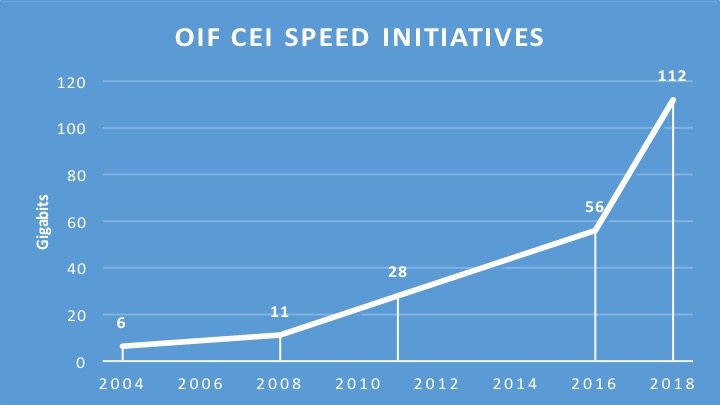 Source: Gazettabyte, OIF data. The year 2018 is an estimate.
The OIF is an industry organisation whose members include telcos, data centre operators, equipment makers and component companies. The OIF undertakes projects that range from high-speed interfaces, optical modules and flexible Ethernet through to programmable interfaces for Transport SDN. Each OIF project culminates in a published Implementation Agreement.
According to David Stauffer, of Kandou Bus and the OIF’s Physical and Link Layer Working Group Chair, the 112G multi-chip module initiative builds on earlier OIF work on a 56-gigabit ultra-short-reach (USR) interface that first addressed die-to-die communication. "We realised that there seems to be more than one application," says Stauffer. "The 112G project is expanded for these applications such that we will possibly end up with different solutions rather than just one."
Multi-chip modules
It was during the 56G USR work that the OIF first heard from members about the challenges of designing a system-on-chip and the idea of taking functions off-chip. High-capacity Ethernet switch chips, for example, are becoming so complex that future designs will not be able to support the long-reach serialisers-deserialisers (SerDes) circuits used for input-output due to the resulting design exceeding the chip's power constraints. “They [chip makers] were starting to think about offloading functions such as SerDes from the system-on-chip,” says Stauffer.
State-of-the-art chip designs can also include functions that occupying significant die area. “To better optimise chip and system costs, people are starting to think about the concept of breaking up the system-on-chip into multiple chips that are better optimised for cost and yield,” says Stauffer. He cites as an example a next-generation system-on-chip that interfaces to long-reach SerDes or optics, performs sensor processing and has significant on-board logic.
 David StaufferThe logic functions of such a chip are best implemented using an advanced 7nm CMOS process, yet SerDes design are not implemented in 7nm and won't be for some time yet. In turn, the sensor array may not even be implemented using a logic process. And if the logic circuitry occupies a significant die area, it may be more economical to split the logic into two chips, each of which will yield better. “Then I have a need for all these interfaces between these chips,” says Stauffer,
He stresses that the interfaces are split based on the the type of technology and on the size of the individual dies; the dies are not partitioned to minimise the bandwidth between them. This can result in significant bandwidth - terabits of capacity - between chips in the module. And to be cost-effective, the interfaces must be very low power.
Accordingly, interfaces between two logic chips or the logic function and the sensor array can require high bandwidth whereas interfaces to the SerDes may be a single lane and have different requirements in how it is clocked. “So there is some divergence in what may be the requirements,” says Stauffer. “The multi-chip module project allows for the fact that we may end up with two solutions.”
The OIF does not list companies involved in its projects. Kandou Bus is clearly one involved in the multi-chip module work, says Stauffer, and he points to similar work his company has done with Marvell but at lower rates. But a recent story in EETimes lists several companies.
Applications
Stauffer says there are several high-performance computing companies that are designing very high-end processing systems using new architectures. “They are going to use this stuff [multi-chip modules and 100G-plus interfaces] before it trickles down to the data centre,” he says.
For applications requiring sensor arrays, the sampling and control loops needed mean that in some cases the interface will need to support terabits-per-second of capacity, says Stauffer; the overall interface speed depending on the number of sensors in the array and the rate at which they sample.
The OIF ultra-short-reach interface is expected to work up to 116Gbps. Some members also want the interface to drive optical devices. “There is going to be a single lane interface at 100G-plus and others that consist of many parallel lanes,” says Stauffer.
The interface will operate over distances of 1cm to 2cm depending on the interposer technology used in the multi-chip module. Using an organic interposer will enable a reach of up to 2cm whereas a silicon interposer the distances will be 1cm or less.
A silicon interposer can be seen as a chip designed solely to interconnect the chips that sit on top, says Stauffer. The advantage of a silicon interposer is that it can supports thousands of input-outputs. But depending on its size and yield, the silicon interposer can be expensive. It also has higher-loss channels, explaining its shorter 1cm reach.
In contrast, an organic interposer is more in line with traditional multi-chip modules, says Stauffer. The interconnect density of an organic interposer is less than a silicon one due to the relatively large pad pitches it uses but the organic interposer is cheaper and has a lower insertion loss. “The OIF is designing something that is suitable for both,” says Stauffer.
No timetable has been given as to the duration of the multi-chip module interface work. But Stauffer says there are companies that would use the electrical interface now if it were available.
OIF starts work on a terabit-plus CFP8-ACO module
The Optical Internetworking Forum (OIF) has started a new analogue coherent optics (ACO) specification based on the CFP8 pluggable module.
The CFP8 is the latest is a series of optical modules specified by the CFP Multi-Source Agreement and will support the emerging 400 Gigabit Ethernet standard.
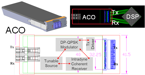
 Karl GassAn ACO module used for optical transport integrates the optics and driver electronics while the accompanying coherent DSP-ASIC residing on the line card.
Systems vendors can thus use their own DSP-ASIC, or a merchant one if they don’t have an in-house design, while choosing the coherent optics from various module makers. The optics and the DSP-ASIC communicate via a high-speed electrical connector on the line card.
ACO design
The OIF completed earlier this year the specification of the CFP2-ACO.
Current CFP2-ACO modules support single-wavelength transmission rates from 100 gigabit to 250 gigabit depending on the baud rate and modulation scheme used. The goal of the CFP8-ACO is to support up to four wavelengths, each capable of up to 400 gigabit-per-second transmissions.
This project is going to drive innovation
“This isn’t something there is a dire need for now but the projection is that this will be needed in two years’ time,” says Karl Gass of Qorvo and the OIF Physical and Link Layer Working Group optical vice chair.
OIF members considered several candidate optical modules for the next-generation ACO before choosing the CFP8. These included the existing CFP2 and the CFP4. There were some proponents for the QSFP but its limited size and power consumption is problematic when considering long-haul applications, says Gass.
 Source: Finisar
One difference between the CFP2 and CFP8 modules is that the electrical connector of the CFP8 supports 16 differential pairs while the CFP2 connector supports 10 pairs.
“Both connectors have similar RF performance and therefore can handle similar baud rates,” says Ian Betty of Ciena and OIF board member and editor of the CFP2-ACO Implementation Agreement. To achieve 400 gigabit on a wavelength for the CFP8-ACO, the electrical connector will need to support 64 gigabaud.
Betty points out that for coherent signalling, four differential pairs per optical carrier are needed. “This is independent of the baud rate and the modulation format,” says Betty.
So while it is not part of the existing Implementation Agreement, the CFP2-ACO could support two optical carriers while the CFP8 will support up to four carriers.
“This is only the electrical connector interface capacity,” says Betty. “It does not imply it is possible to fit this amount of optics and electronics in the size and power budget.” The CFP8 supports a power envelope of 20W compared to 12W of the CFP2.
 The CFP2-ACO showing the optical building blocks and the electrical connector linking the module to the DSP-ASIC. Source: OIF
The CFP8 occupies approximately the same area as the CFP2 but is not as tall such that the module can be doubled-stacked on a line card for a total of 16 CFP8-ACOs on a line card.
Given that the CFP8 will support up to four carriers per module - each up to 400 gigabit - a future line card could support 25.6 terabits of capacity. This is comparable to the total transport capacity of current leading dense WDM optical transport systems.
Rafik Ward, vice president of marketing at Finisar, says such a belly-to-belly configuration of the modules provides future-proofing for next-generation lineside interfaces. “Having said that, it is not clear when, or how, we will be able to technically support a four-carrier coherent solution in a CFP8 form factor,” says Ward.
Oclaro stresses that such a high total capacity implies that sufficient coherent DSP silicon can fit on the line card. Otherwise, the smaller-height CFP8 module may not enable the fully expected card density if the DSP chips are too large or too power-hungry.
OIF goal
Besides resulting in a higher density module, a key OIF goal of the work is to garner as much industry support as possible to back the CFP8-ACO. “How to create the quantity of scale so that deployment becomes less expensive and therefore quicker to implement,” says Gass.
The OIF expects the work to be similar to the development of the CFP2-ACO Implementation Agreement. But one desired difference is to limit the classes associated with the module. The CFP2-ACO has three class categories based on whether the module has a limited and linear output. “The goal of the CFP8-ACO is to limit the designs to single classes per wavelength count,” says Gass.
Gass is looking forward to the CFP8-ACO specification work. Certain standards efforts largely involve making sure components fit into a box whereas the CFP8-ACO will be more engaging. “This project is going to drive innovation and that will drive some technical work,” says Gass.
OIF document aims to spur line-side innovation
 The CFP2-ACO. Source: OIF
The pluggable CFP2-ACO houses the coherent optics, known as the analogue front end. The components include the tuneable lasers, modulation, coherent receiver, and the associated electronics - the drivers and the trans-impedance amplifier. The Implementation Agreement also includes the CFP2-ACO's high-speed electrical interface connecting the optics to the coherent DSP chip that sits on the line card.
One historical issue involving the design of innovative optical components into systems has been their long development time, says Ian Betty of Ciena, and OIF board member and editor of the CFP2-ACO Implementation Agreement. The lengthy development time made it risky for systems vendors to adopt such components as part of their optical transport designs. Now, with the CFP2-ACO, much of that risk is removed; system vendors can choose from a range of CFP2-ACO suppliers based on the module's performance and price.
Implementation Agreement
Much of the two-year effort developing the Implementation Agreement involved defining the management interface to the optical module. "This is different from our historical management interfaces," says Betty. "This is much more bare metal control of components."
For 7x5-inch and 4x5-inch MSA transponders, the management interface is focused on system-level parameters, whereas for the CFP2-ACO, lower-level optical parameters are accessible given the module's analogue transmission and receive signals.
"A lot of the management is to interrogate information about power levels, or adjusting transfer functions with pre-emphasis, or adjusting drive levels on drivers internal to the device, or asking for information: 'Have you received my RF signal?'," says Betty. "It is very much a lower-level interface because you have separated between the DSP and the optical interface."
The Implementation Agreement's definitions for the CFP2-ACO are also deliberately abstract. The optical technology used is not stated, nor is the module's data rate. "The module has no information associated with the system level - if it is 16-QAM or QPSK [modulation] or what the dispersion is," says Betty.
This is a strength, he says, as it makes the module independent of a data rate and gives it a larger market because any coherent ASIC can make use of this analogue front end. "It lets the optics guys innovate, which is what they are good at," says Betty.
Innovation
The CFP2-ACO is starting to be adopted in a variety of platforms. Arista Networks has added a CFP2-ACO line card to its 7500 data centre switches while several optical transport vendors are using the module for their data centre interconnect platforms.
One obvious way optical designers can innovate is by adding flexible modulation formats to the CFP2-ACO. Coriant's Groove G30 data centre interconnect platform uses CFP2-ACOs that support polarisation-multiplexed, quadrature phase-shift keying (PM-QPSK), polarisation-multiplexed, 8-state quadrature amplitude modulation (PM-8QAM) and PM-16QAM, delivering 100, 150 and 200 gigabit-per-second transmission, respectively. Coriant says the CFP2-ACOs it uses are silicon photonics and indium phosphide based.
Cisco Systems uses CFP2-ACO modules for its first data centre interconnect product, the NCS 1002. The system can use a CFP2-ACO with a higher baud rate to deliver 250 gigabit-per-second using a single carrier and PM-16QAM.
 Ian BettyThe CFP2-ACO enables a much higher density line-side solution than other available form factors. The Groove G30, for example, fits eight such modules on one rack-unit line card. "That is the key enabler that -ACOs give," says Betty.
And being agnostic to a particular DSP, the CFP2-ACO enlarges the total addressable market. Betty hopes that by being able to sell the CFP2-ACO to multiple systems vendors, the line-side optical module players can drive down cost.
Roadmap
Betty says that the CFP2-ACO may offer the best route to greater overall line side capacity rather than moving to a smaller form factor module in future. He points out that in the last decade, the power consumption of the optics has gone down from some 16W to 12W. He does not foresee the power consumption coming down further to the 6W region that would be needed to enable a CFP4-ACO. "The size [of the CFP4] with all the technology available is very doable," says Betty. "But there is not an obvious way to make it [the optics] 6W."
The key issue is the analogue interface which determines what baud rate and what modulation or level of constellation can be put through a module. "The easiest way to lump all that together is with an implementation penalty for the optical front end," says Betty. "If you make the module smaller, you might have a higher implementation penalty, and with this penalty, you might not be able to put a higher constellation through it."
In other words, there are design trade-offs: the data rates supported by the CFP2 modules may achieve a higher overall line-side rate than more, smaller modules, each supporting a lower maximum data rate due to a higher implementation penalty.
"What gets you the ultimate maximum density of data rate through a given volume?" says Betty. "It is not necessarily obvious that making it smaller is better."
Could a CFP2-ACO support 32-QAM and 64-QAM? "The technical answer is what is the implementation penalty of the module?" says Betty. This is something that the industry will answer in time.
"This isn't the same as client optics where there is a spec, you do the spec and there are no brownie points for doing better than the spec, so all you can compete on is cost," says Betty. "Here, you can take your optical innovation and compete on cost, and you can also compete by having lower implementation penalties."
OIF moves to raise coherent transmission baud rate
"We want the two projects to look at those trade-offs and look at how we could build the particular components that could support higher individual channel rates,” says Karl Gass of Qorvo and the OIF physical and link layer working group vice chair, optical.
 Karl Gass
The OIF members, which include operators, internet content providers, equipment makers, and optical component and chip players, want components that work over a wide bandwidth, says Gass. This will allow the modulator and receiver to be optimised for the new higher baud rate.
“Perhaps I tune it [the modulator] for 40 Gbaud and it works very linearly there, but because of the trade-off I make, it doesn’t work very well anywhere else,” says Gass. “But I’m willing to make the trade-off to get to that speed.” Gass uses 40 Gbaud as an example only, stressing that much work is required before the OIF members choose the next baud rate.
"We want the two projects to look at those trade-offs and look at how we could build the particular components that could support higher individual channel rates”
The modulator and receiver optimisations will also be chosen independent of technology since lithium niobate, indium phosphide and silicon photonics are all used for coherent modulation.
The OIF has not detailed timescales but Gass says projects usually take 18 months to two years.
Meanwhile, the OIF has completed two projects, the specification outputs of which are referred to as implementation agreements (IAs).
One is for integrated dual polarisation micro-intradyne coherent receivers (micro-ICR) for the CFP2. At OFC 2015, several companies detailed first designs for coherent line side optics using the CFP2 module.
The second completed IA is the 4x5-inch second-generation 100 Gig long-haul DWDM transmission module.
OIF shows 56G electrical interfaces & CFP2-ACO
 “The most important thing for everyone is power consumption on the line card”
The OIF - an industry organisation comprising communications service providers, internet content providers, system vendors and component companies - is developing the next common electrical interface (CEI) specifications. The OIF is also continuing to advance fixed and pluggable optical module specifications for coherent transmission including the pluggable CFP2 (CFP2-ACO).
“These are major milestones that the [demonstration] efforts are even taking place,” says Nathan Tracy, a technologist at TE Connectivity and the OIF technical committee chair.
Tracy stresses that the CEI-56G specifications and the CFP2-ACO remain works in progress. “They are not completed documents, and what the demonstrations are not showing are compliance and interoperability,” he says.
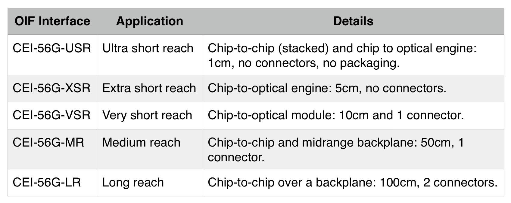
Five CEI-56G specifications are under development, such as platform backplanes and links between a chip and an optical engine on a line card (see Table below).
Moving from the current 28 Gig electrical interface specifications to 56 Gig promises to double the interface capacity and cut electrical interface widths by half. “If we were going to do 400 Gigabit with 25 Gig channels, we would need 16 channels,” says Tracy. “If we can do 50 Gig, we can get it down to eight channels.” Such a development will enable chassis to carry more traffic and help address the continual demand for more bandwidth, he says.
But doubling the data rate is challenging. “As we double the rate, the electrical loss or attenuation of the signal travelling across a printed circuit board is significantly impacted,” says Tracy. “So now our reaches have to get a lot shorter, or the silicon that sends and receives has to improve to significant higher levels.”
One of the biggest challenges in system design is thermal management
Moreover, chip designers must ensure that the power consumption of their silicon do not rise. “We have to be careful as to what the market will tolerate, as one of the biggest challenges in system design is thermal management,” says Tracy. “We can’t just do what it takes to get to 56 Gigabit.”
To this aim, the OIF is pursuing two parallel tracks: using 56 Gigabit non-return-to-zero (NRZ) signalling and 4-level pulse amplitude modulation (PAM-4) which encodes two bits per symbol such that a 28 Gbaud signalling rate can be used. The 56 Gig NRZ uses simpler signalling but must deal with the higher associated loss, while PAM-4 does not suffer the same loss as it is similar to existing CEI-28 channels used today but requires a more complex design.
“Some [of the five CEI-56G specifications] use NRZ, some PAM-4 and some both,” says Tracy. The OIF will not say when it will complete the CEI-56G specifications. However, the projects are making similar progress while the OIF is increasing its interactions with other industry standards groups to shorten the overall timeline.
 Source: OIF, Gazettabyte
Two of the CEI-56G specifications cover much shorter distances: the Extra Short Reach (XSR) and Ultra Short Reach (USR). According to the OIF, in the past it was unclear that the industry would benefit from interoperability for such short reaches.
“What is different at 56 Gig is that architectures are fundamentally being changed: higher data rates, industry demand for higher levels of performance, and changing fabrication technologies,” says Tracy. Such fabrication technologies include 3D packaging and multi-chip modules (MCMs) where silicon dies from different chip vendors may be connected within the module.
The XSR interface is designed to enable higher aggregate bandwidth on a line card which is becoming limited by the number of pluggable modules that can be fitted on the platform’s face plate. Density can be increased by using mid-board optics (an optical engine) placed closer to a chip. Here, fibre from the optical engine is fed to the front plate increasing the overall interface capacity.
The USR interface is to support stackable ICs and MCMs.
All are coming together in this pre-competitive stage to define the specifications, yet, at the same time, we are all fierce competitors
“The most important thing for everyone is power consumption on the line card,” says Tracy. “If you define these very short reach interfaces in such a way that these chips do not need as much power, then we have helped to enable the next generation of line card.”
The live demonstrations at OFC include a CEI-56G-VSR-NRZ channel, a CEI-56G-VSR-PAM QSFP compliance board, CEI-56G-MR/LR-PAM and CEI-56G-MR/LR-NRZ backplanes, and a CEI-56G-MR-NRZ passive copper cable.
The demonstrations reflects what OIF members are willing to show, as some companies prefer to keep their work private. “All are coming together in this pre-competitive stage to define the specifications, yet, at the same time, we are all fierce competitors,” says Tracy.
CFP2-ACO
Also on display is working CFP2 analogue coherent optics (CFP2-ACO). The significance of coherent optics in a pluggable CFP2 is the promise of higher-density line cards. The CFP is a much bigger module and at most four can be fitted on a line card, while with the smaller CFP2, with its lower power consumption, up to eight modules are possible.
Using the CFP2-ACO, the coherent DSP-ASIC is external to the CFP2 module. Much work has been done to ensure that the electrical interface can support the analogue signalling between the CFP2 optics and the on-board DSP-ASIC, says Tracy.
At OFC, several companies have unveiled their CFP2-ACO products including Finisar, Fujitsu Optical Components, Oclaro and NEC, while Clariphy has announced a single-board reference design that includes its CL20010 DSP-ASIC and a CFP2-ACO slot.
OIF demonstrates its 25 Gig interfaces are ready for use
The Open Internetworking Forum (OIF) has demonstrated its specified 25 and 28 Gigabit-per-second (Gbps) electrical interfaces working across various vendors' 100 Gigabit modules and ICs.
 "The infrastructure over the backplane is maturing to the point of 25 Gig; you don't need special optical backplanes" John Monson, Mosys
"The ecosystem is maturing," says John Monson, vice president of marketing at Mosys, one of the 11 firms participating in the demonstrations. "The demos are not just showing the electrical OIF interfaces but their functioning between multiple vendors, with optical standards running across them at 100 Gig."
The demonstrations - using the CFP2, QSFP and CPAK optical modules and the 28Gbps CEI-28G-VSR module-to-chip electrical interface - set the stage for higher density 400 and 800 Gigabit line cards, says Monson. The CEI-28G-VSR is specified for up to 10dB of signal loss, equating to some 4 to 6 inches of trace on a high-quality material printed circuit board.
Higher density system backplanes are also ready using the OIF's CEI-25G-LR interface. "Until I get backplanes capable of high rates, there are just too many pins at 10 Gig to support 800 Gig and Terabit [line card] solutions," says Monson.
The ECOC demonstrations include two 100Gbps modules linked over fibre. "You have two CFP2 modules, from different vendors, running at 4x28Gbps OTN [Optical Transport Network] rates over 10km," says Monson.
On the host side, the CEI-28G-VSR interface sits between a retimer inside the CFP2 module and a gearbox chip that translates between 25Gbps and the 10Gbps lanes that link a framer or a MAC IC on the line card.
The demonstrations cover different vendors' gearbox ICs talking to different optical module makers' CFP2s as well as Cisco's CPAK. "We are mixing and matching quite a bit in these demos," says Monson.
The OIF has already started work for the next-generation electrical interfaces that follow the 25 and 28 Gigabit ones
There is also a demo of a QSFP+ module driving active copper cable and one involving two 100 Gigabit SR10 modules and a gearbox IC. Three further demos involve the CEI-25G-LR backplane interface. Lastly, there is a demo involving the thermal modelling of a line card hosting eight slots of the CDFP 400Gbps optical module MSA.
The OIF's CEI-25G-LR is specificed for up to 25dB of loss. The IEEE P802.3bj 100 Gbps Backplane and Copper Cable Task Force is specifying an enhanced backplane electrical interface that supports 35dB of loss using techniques such as forward error correction.
"What the demos say is that the electrical interfaces, at 25 Gig, can be used not just for a 4-6 inch trace, but also high-density backplanes," says Monson. As a result line card density will increase using the smaller form factor 100Gbps optical modules. It also sets the stage for 400 Gig individual optics, says Monson: "The infrastructure over the backplane is maturing to the point of 25 Gig; you don't need special optical backplanes."
Meanwhile, standards work for 400 Gigabit Ethernet is still at an early stage, but proposals for 56Gbps links have been submitted for consideration. "Such a rate would double capacity and reduce the number of pins required on the ASSPs and ASICs," says Monson.
As to how the electrical interface for 400 Gigabit Ethernet will be implemented, it could be 16x25Gbps or 8x50Gbps lanes and will also be influenced by the chosen optical implementation. The OIF has already started work for the next-generation electrical interfaces that follow the 25 and 28 Gigabit ones.
The 11 companies and the two test and measurement companies taking part, as well as the demonstrations, are detailed in an OIF White Paper, click here.
Luxtera's interconnect strategy
Part 1: Optical interconnect
Luxtera demonstrated a 100 Gigabit QSFP optical module at the OFC/NFOEC 2013 exhibition.
 "We're in discussions with a lot of memory vendors, switch vendors and different ASIC providers"
Chris Bergey, Luxtera
The silicon photonics-based QSFP pluggable transceiver was part of the Optical Internetworking Forum's (OIF) multi-vendor demonstration of the 4x25 Gigabit chip-to-module interface, defined by the CEI-28G-VSR Implementation Agreement.
The OIF demonstration involved several optical module and chip companies and included CFP2 modules running the 100GBASE-LR4 10km standard alongside Luxtera's 4x28 Gigabit-per-second (Gbps) silicon photonics-based QSFP28.
Kotura also previewed a 100Gbps QSFP at OFC/NFOEC but its silicon photonics design uses two chips and wavelength-division multiplexing (WDM).
The Luxtera QSFP28 is being aimed at data centre applications and has a 500m reach although Luxtera says up to 2km is possible. The QSFP28 is sampling to initial customers and will be in production next year.
100 Gigabit modules
Current 100GBASE-LR4 client-side interfaces are available in the CFP form factor. OFC/NFOEC 2013 saw the announcement of two smaller pluggable form factors at 100Gbps: the CFP2, the next pluggable on the CFP MSA roadmap, and Cisco Systems' in-house CPAK.
Now silicon photonics player Luxtera is coming to market with a QSFP-based 100 Gigabit interface, more compact than the CFP2 and CPAK.
The QSFP is already available as a 40Gbps interface. The 40Gbps QSFP also supports four independent 10Gbps interfaces. The QSFP form factor, along with the SFP+, are widely used on the front panels of data centre switches.
"The QSFP is an inside-the-data-centre connector while the CFP/CFP2 is an edge of the data centre, and for telecom, an edge router connector," says Chris Bergey, vice president of marketing at Luxtera. "These are different markets in terms of their power consumption and cost."
Bergey says the big 'Web 2.0' data centre operators like the reach and density offered by the 100Gbps QSFP as their data centres are physically large and use flatter, less tiered switch architectures.
"If you are a big systems company and you are betting on your flagship chip, you better have multiple sources"
The content service providers also buy transceivers in large volumes and like that the Luxtera QSFP works over single-mode fibre which is cheaper than multi-mode fibre. "All these factors lead to where we think silicon photonics plays in a big way," says Bergey.
The 100Gbps QSFP must deliver a lower cost-per-bit compared to the 40Gbps QSFP if it is to be adopted widely. Luxtera estimates that the QSFP28 will cost less than US $1,000 and could be as low as $250.
Optical interconnect
Luxtera says its focus is on low-cost, high-density interconnect rather than optical transceivers. "We want to be a chip company," says Bergey.
The company defines optical interconnect as covering active optical cable and transceivers, optical engines used as board-mounted optics placed next to chips, and ASICs with optical SerDes (serialiser/ deserialisers) rather than copper ones.
Optical interconnect, it argues, will have a three-stage evolution: starting with face-plate transceivers, moving to mid-board optics and then ASICS with optical interfaces. Such optical interconnect developments promise lower cost high-speed designs and new ways to architect systems.
Currently optics are largely confined to transceivers on a system׳s front panel. The exceptions are high-end supercomputer systems and emerging novel designs such as Compass-EOS's IP core router.
"The problem with the front panel is the density you can achieve is somewhat limited," says Bergey. Leading switch IC suppliers using a 40nm CMOS process are capable of a Terabit of switching. "That matches really well if you put a ton of QSFPs on the front panel," says Bergey.
But once switch IC vendors use the next CMOS process node, the switching capacity will rise to several Terabits. This becomes far more challenging to meet using front panel optics and will be more costly compared to putting board-mounted optics alongside the chip.
"When we build [silicon photonics] chips, we can package them in QSFPs for the front panel, or we can package them for mid-board optics," says Bergey.
"If it [silicon photonics] is viewed as exotic, it is never going to hit the volumes we aspire to."
The use of mid-board optics by system vendors is the second stage in the evolution of optical interconnect. "It [mid-board optics] is an intermediate step between how you move from copper I/O [input/output] to optical I/O," says Bergey.
The use of mid-board optics requires less power, especially when using 25Gbps signals, says Bergey: “You dont need as many [signal] retimers.” It also saves power consumed by the SerDes - from 2W for each SerDes to 1W, since the mid-board optics are closer and signals need not be driven all the way to the front panel. "You are saving 2W per 100 Gig and if you are doing several Terabits, that adds up," says Bergey.
The end game is optical I/O. This will be required wherever there are dense I/O requirements and where a lot of traffic is aggregated.
Luxtera, as a silicon photonics player, is pursuing an approach to integrate optics with VLSI devices. "We're in discussions with a lot of memory vendors, switch vendors and different ASIC providers," says Bergey.
Silicon photonics fab
Last year STMicroelectronics (ST) and Luxtera announced they would create a 300mm wafer silicon photonics process at ST's facility in Crolles, France.
Luxtera expects that line to be qualified, ramped and in production in 2014. Before then, devices need to be built, qualified and tested for their reliability.
"If you are a big systems company and you are betting on your flagship chip, you better have multiple sources," says Bergey. "That is what we are doing with ST: it drastically expands the total available market of silicon photonics and it is something that ST and Luxtera can benefit from.”
Having multiple sources is important, says Bergey: "If it [silicon photonics] is viewed as exotic, it is never going to hit the volumes we aspire to."
Part 2: Bell Labs on silicon photonics click here
Part 3: Is silicon photonics an industry game-changer? click here
The role of software-defined networking for telcos
The OIF's Carrier Working Group is assessing how software-defined networking (SDN) will impact transport. Hans-Martin Foisel, chair of the OIF working group, explains SDN's importance for operators.
Briefing: Software-defined networking
Part 1: Operator interest in SDN
 "Using SDN use cases, we are trying to derive whether the transport network is ready or if there is some missing functionality"
Hans-Martin Foisel, OIF
Hans-Martin Foisel, of Deutsche Telekom and chair of the OIF Carrier Working Group, says SDN is of great interest to operators that view the emerging technology as a way of optimising all-IP networks that increasingly make use of data centres.
"Software-defined networking is an approach for optimising the network in a much larger sense than in the past," says Foisel whose OIF working group is tasked with determining how SDN's requirements will impact the transport network.
Network optimisation remains an ongoing process for operators. Work continues to improve the interworking between the network's layers to gain efficiencies and reduce operating costs (see Cisco Systems' intelligent light).
With SDN, the scope is far broader. "It [SDN] is optimising the network in terms of processing, storage and transport," says Foisel. SDN takes the data centre environment and includes it as part of the overall optimisation. For example, content allocation becomes a new parameter for network optimisation.
Other reasons for operator interest in SDN, says Foisel, include optimising operation support systems (OSS) software, and the characteristic most commonly associated with SDN, making more efficient use of the network's switches and routers.
"A lot of carriers are struggling with their OSSes - these are quite complex beasts," he says. "With data centres involved, you now have a chance to simplify your IT as all carriers are struggling with their IT."
The Network Functions Virtualisation (NFV) industry specification group is a carrier-led initiative set up in January by the European Telecommunications Standards Institute (ETSI). The group is tasked with optimising software components, the OSSes, involved for processing, storage and transport.
The initiative aims to make use of standard servers, storage and Ethernet switches to reduce the varied equipment making up current carrier networks to improve service innovation and reduce the operators' capital and operational expenditure.
The NFV and SDN are separate developments that will benefit each other. The ETSI group will develop requirements and architecture specifications for the hardware and software infrastructure needed for the virtualized functions, as well as guidelines for developing network functions.
The third reason for operator interest in SDN - separating management, control and data planes - promises greater efficiencies, enabling network segmentation irrespective of the switch and router deployments. This allows flexible use the network, with resources shifted based on particular user requirements.
"Optimising the network as a whole - including the data centre services and applications - is a concept, a big architecture," says Foisel. "OpenFlow and the separation of data, management and control planes are tools to achieve them."
OpenFlow is an open standard implementation of the SDN concept. The OpenFlow protocol is being developed by the Open Networking Foundation, an industry body that includes Google, Facebook and Microsoft, telecom operators Verizon, NTT, Deutsche Telekom, and various equipment makers.
Transport SDN
The OIF Working Group will identify how SDN impacts the transport network including layers one and two, networking platforms and even components. By undertaking this work, the operators' goal is to make SDN "carrier-grade'.
Foisel admits that the working group does not yet know whether the transport layer will be impacted by SDN. To answer the question, SDN applications will be used to identify required transport SDN functionalities. Once identified, a set of requirements will be drafted.
"Using SDN use cases, we are trying to derive whether the transport network is ready or if there is some missing functionality," says Foisel.
The work will also highlight any areas that require standardisation, for the OIF and for other standards bodies, to ensure future SDN interworking between vendors' solutions. The OIF expects to have a first draft of the requirements by July 2013.
"In the transport network we are pushed by the mobile operators but also by the over-the-top applications to be faster and be more application-aware," says Foisel. "With SDN we have a chance to do so."
Part 2: Hardware for SDN
OIF promotes uni-fabric switches & 100G transmitter
 The OIF's OTN implementation agreement (IA) allows a packet fabric to also switch OTN traffic. The result is that operators can now use one switch for both traffic types, aiding IP/ Ethernet and OTN convergence. Source: OIF
Improving the switching capabilities of telecom platforms without redesigning the switch as well as tinier 100 Gigabit transmitters are just two recent initiatives of the Optical Internetworking Forum (OIF).
The OIF, the industry body tackling design issues not addressed by the IEEE and International Telecommunication Union (ITU) standards bodies, has just completed its OTN-over-Packet-Fabric protocol that enables optical transport network (OTN) traffic to be carried over a packet switch. The protocol works by modifying the line cards at the switch's input and output, leaving the switch itself untouched (see diagram above).
In contrast, the OIF is starting a 100 Gigabit-per-second (Gbps) transmitter design project dubbed the integrated dual-polarisation quadrature modulated transmitter assembly (ITXA). The Working Group aims to expand the 100Gbps applications with a transmitter design half the size of the OIF's existing 100Gbps transmitter module.
The Working Group also wants greater involvement from the system vendors to ensure the resulting 100 Gig design is not conservative. "We joke about three types of people that attend these [working group] meetings," says Karl Gass, the OIF’s Physical and Link Layer Working Group vice-chair. "The first group has something they want to get done, the second group has something already and they don't want something to get done, and the third group want to watch." Quite often it is the system vendors that fall into this third group, he says.
OTN-over-Packet-Fabric protocol
The OTN protocol enable a single switch fabric to be used for both traffic types - packets and time-division multiplexed (TDM) OTN - to save cost for the operators.
"OTN is out there while Ethernet is prevalent," says Winston Mok, technical author of the OTN implementation agreement. "What we would like to do is enable boxes to be built that can do both economically."
 The existing arrangement where separate packet and OTN time-division multiplexing (TDM) switches are required. Source: OIF
Platforms using the protocol are coming to market. ECI Telecom says its recently announced Apollo family is one of the first OTN platforms to use the technique.
The protocol works by segmenting OTN traffic into a packet format that is then switched before being reconstructed at the output line card. To do this, the constant bit-rate OTN traffic is chopped up so that it can easily go through the switch as a packet. "We want to keep the [switch] fabric agnostic to this operation," says Mok. "Only the line cards need to do the adaptations."
The OTN traffic also has timing information which the protocol must convey as it passes through the switch. The OIF's solution is to vary the size of the chopped-up OTN packets. The packet is nominally 128-bytes long. But the size will occasionally be varied to 127 and 126 bytes as required. These sequences are interpreted at the output of the switch as rate information and used to control a phase-locked loop.
Mok says the implementation agreement document that describes the protocol is now available. The protocol does not define the physical layer interface connecting the line card to the switch, however. "Most people have their own physical layer," says Mok.
100 Gig ITXA
The ITXA project will add to the OIF's existing integrated transmitter document. The original document addresses the 100 Gigabit transmitter for dual-polarisation, quadrature phase-shift keying (DP-QPSK) for long-haul optical transmission. The OIF has also defined 100Gbps receiver assembly and tunable laser documents.
The latest ITXA Working Group has two goals: to shrink the size of the assembly to lower cost and increase the number of 100Gbps interfaces on a line card, and to expand the applications to include metro. The ITXA will still address 100Gbps coherent designs but will not be confined to DP-QPSK, says Gass.
"We started out with a 7x5-inch module and now there is interest from system vendors and module makers to go to smaller [optical module] form factors," says Gass. "There is also interest from other modulator vendors that want in on the game."
The reduce size, the ITXA will support other modulator technologies besides lithium niobate that is used for long-haul. These include indium phosphide, gallium arsenide and polymer-based modulators.
Gass stresses that the ITXA is not a replacement for the current transmitter implementation. "We are not going to get the 'quality' that we need for long-haul applications out of other modulator technologies," he says. "This is not a Gen II [design].
The Working Group's aim is to determine the 'greatest common denominator' for this component. "We are trying to get the smallest form factor possible that several vendors can agree on," says Gass. "To come out with a common pin out, common control, common RF (radio frequency) interface, things like that."
Gass says the work directions are still open for consideration. For example, adding the laser with the modulator. "We can come up with a higher level of integration if we consider adding the laser, to have a more integrated transmitter module," says Gass.
As for wanting great system-vendor input, the Working Group wants more of their system-requirement insights to avoid the design becoming too restrictive.
"You end up with component vendors that do all the work and they want to be conservative," says Gass. "The component vendors don't want to push the boundaries as they want to hit the widest possible customer base."
Gass expects the ITXA work to take a year, with system demonstrations starting around mid-2013.