Manish Mehta, vice president of marketing and operations optical systems division, Broadcom
Tencent is the first hyperscaler to announce it is deploying a co-packaged optics switch chip
Tencent will use Broadcom’s Humboldt that combines its 25.6-terabit Tomahawk 4 switch chip with four optical engines, each 3.2 terabit-per-second (Tbps)
Part 2: Broadcom’s co-packaged optics
Tencent will use Broadcom’s Tomahawk 4 switch chip co-packaged with optics for its data centres.
“We are now partnered with the hyperscaler to deploy this in a network,” says Manish Mehta, vice president of marketing and operations optical systems division, Broadcom. “This is a huge step for co-packaged optics overall.”
Broadcom demonstrated a working version of a Humboldt switch at OFC earlier this year.
The Chinese hyperscaler will use Broadcom’s 25.6Tbps Tomahawk 4 Humboldt, a hybrid design where half of the chip’s input-output (I/O) is optical and half is the chip’s serialisers-deserialisers (serdes) that connect to pluggable modules on the switch’s front panel.
Four Broadcom 3.2-terabit silicon photonics-based optical engines are co-packaged alongside the Tomahawk 4 chip to implement 12.8Tbps of optical I/O.
Broadcom demonstrated a working version of a Humboldt switch at OFC earlier this year.
Co-packaged optics
Broadcom started its co-packaged optics development work in 2019.
“One of the reasons for our investment in co-packaged optics was that we did see firsthand the ongoing limits of copper interconnect being approached,” says Mehta.
The transmission reach of copper links continues to shrink as the signalling speed has increased from 25 gigabits-per-second (Gbps) non-return to zero (NRZ) to PAM-4 (4-level pulse amplitude modulation) based signalling at 56Gbps, 112Gbps and, in the coming years, 224Gbps. Power consumption is also rising with each speed hike.
Broadcom says data centres now use 1 million optical interconnects, but that much of the connectivity is still copper-based, linking adjacent racks and equipment within the rack.
“Hyperscalers spend ten times more on interconnects than switching silicon,” says Mehta. Given these trends, there needs to be a continual improvement in the power profile, cost and scaled manufacturing of optical interconnect, he says.
In the short term, what is driving interest in co-packaged optics is overcoming the limitations of copper, says Broadcom.
In early 2021, Broadcom detailed at a JP Morgan event its co-packaged optics roadmap. Outlined was the 25.6-terabit Humboldt to be followed by Bailly, a 51.2-terabit all co-packaged optics design using Broadcom’s Tomahawk 5 switch chip which is now sampling.
Humboldt uses DR4 (4×100-gigabit using 4 fibres) whereas the 51.2-terabit Bailly will add multiplexing-demultiplexing and use the FR4 specification (4×100-gigabit wavelengths per fibre).
Technology and partners
Broadcom’s in-house technology includes lasers (VCSELs and EMLs), mixed-signal expertise (trans-impedance amplifiers and drivers), and silicon photonics, as well as its switch chips.
Broadcom uses a remote laser source for its co-packaged optics design. Placing the laser away from the package (the switch chip and optics) means no cooling is needed.
Broadcom is working with 15 partners to enable its co-packaged optics, highlighting the breadth of expertise required and the design complexity.
A clos architecture in the data centre showing top-of-rack (ToR) and layers of aggregation switches. Source: Broadcom
There are two prominent use cases for the hybrid I/O Humboldt.
One is for top-of-rack switches, where the electrical interfaces support short-reach copper links connecting the servers in a rack, while the optical links connect the top-of-rack box to the next layer of aggregation switching.
The second use is at the aggregation layer, where the electrical I/O connects other switches in the rack while the optical links connect to switch layers above or below the aggregation layer.
“There is a use case for having pluggable ports where you can deploy low-cost direct-attached copper,” says Mehta.
Broadcom says each data centre operator will have their own experience with their manufacturing partners as they deploy co-packaged optics. Tencent has decided to enter the fray with 25.6-terabit switches.
“It is not just Broadcom developing the optical solution; it is also ensuring that our manufacturing partner is ready to scale,” says Mehta.
Ruijie Networks is making the two-rack-unit (2RU) switch platform for Tencent based on Broadcom’s co-packaged optics solution. The co-packaged optics interfaces are routed to 16 MPO connectors while the switch supports 32, 400-gigabit QSFP112 modules.
“It’s always important to have your lead partner [Tencent] for any deployment like this, someone you’re working closely with to get it to market,” says Mehta. “But there is interest from other customers as well.”
Cost and power benefits
Broadcom says co-packaged optics will lower the optical cost-per-bit by 40 per cent while the system (switch platform) power savings will be 30 per cent.
Humboldt more than halves the power compared to using pluggables. Broadcom’s co-packaged optics consumes 7W for each 800-gigabits of bandwidth, whereas an equivalent 800-gigabit optical module consumes 16-18W.
Its second-generation design will embrace 5nm CMOS rather than 7nm and still more than halve the power: an 800-gigabit pluggable will consume 14-15W, whereas it will be 5.5W for the same co-packaged optics bandwidth.
Broadcom will move to CMOS for its second-generation electrical IC; it uses silicon germanium at present.
Power and operational cost savings are a longer-term benefit for data centre operators, says Broadcom. A more immediate concern is the growing challenge of managing the thermal profile when designing switching systems. “The amount of localised heat generation of these components is making systems quite challenging,” says Mehta.
A co-packaged design eliminates pluggables, making system design easier by improving airflow via the front panel and reducing the power required for optical interconnect.
“They’ve been telling us this directly,” says Mehta. “It’s been a pretty good testimonial to the benefits they can see for system design and co-packaged optics.”
Roadmap
At OFC 2022, Broadcom also showed a mock-up of Bailly, a 51.2 terabit switch chip co-packaged with eight 6.4Tbps optical engines.
Broadcom will offer customers a fully co-packaged optics Tomahawk 5 design but has not given a date.
Since Broadcom has consistently delivered a doubling of switch silicon capacity every 24 months, a 102.4-terabit Tomahawk 6 is scheduled to sample in the second half of 2024.
That timescale suggests it will be too early to use 224Gbps serdes being specified by the OIF. Indeed, Mehta believes 112Gbps serdes will have “a very long life”.
That would require the next-generation 102.2Tbps to integrate 1024, 100Gbps serdes on a die. Or, if that proves too technically challenging, then, for the first time, Broadcom’s switching ASIC may no longer be a monolithic die.
Broadcom’s networking group is focused on high-speed serial electrical interfaces. But the company is encouraged by developments such as the open standard UCIe for package interconnect, which looks at slower, wider parallel electrical interfaces to support chiplets. UCIe promises to benefit co-packaged optics.
Broadcom’s view is that it is still early with many of these design challenges.
“Our goal is to understand when we need to be ready and when we need to be launching our silicon on the optical side,” says Mehta. “That’s something we are working towards; it’s still not clear yet.”
Broadcom will offer a co-packaged version combining the chip with eight 6.4 terabit-per-second (Tbps) optical engines
Part 1: Broadcom’s Tomahawk 5
Broadcom is sampling the world’s first 51.2-terabit switch chip.
With the Tomahawk 5, Broadcom continues to double switch silicon capacity every 24 months; Broadcom launched the first 3.2-terabit Tomahawk was launched in September 2014.
“Broadcom is once again first to market at 51.2Tbps,” says Bob Wheeler, principal analyst at Wheeler’s Network. “It continues to execute, while competitors have struggled to deliver multiple generations in a timely manner.”
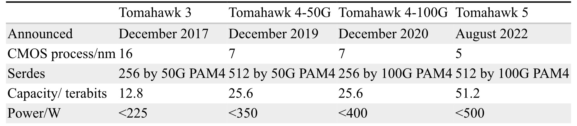
Tomahawk family
Hyperscalers use the Tomahawk switch chip family in their data centres.
Broadcom launched the 25.6-terabit Tomahawk 4 in December 2019. The chip uses 512 serdes, but these are 50-gigabit PAM-4. At the time, 50-gigabit PAM-4 matched the optical modules’ 8-channel input-output (I/O).
Certain hyperscalers wanted to wait for 400-gigabit optical modules using four 100-gigabit PAM-4 electrical channels, so, in late 2020, Broadcom launched the Tomahawk4-100G switch chip, which employs 256, 100-gigabit PAM-4 serdes.
Tomahawk 5 doubles the 100-gigabit PAM-4 serdes to 512. However, given that 200-gigabit electrical interfaces are several years off, Broadcom is unlikely to launch a second-generation Tomahawk 5 with 256, 200-gigabit PAM-4 serdes.
Source: Broadcom, Gazettabyte
Switch ICs
Broadcom has three switch chip families: Trident, Jericho and the Tomahawk.
The three switch chip families are needed since no one switch chip architecture can meet all the markets’ requirements.
With its programable pipeline, Trident targets enterprises, while Jericho targets service providers.
According to Peter Del Vecchio, Broadcom’s product manager for the Tomahawk and Trident lines, there is some crossover. For example, certain hyperscalers favour the Trident’s programmable pipeline for their top-of-rack switches, which interface to the higher-capacity Tomahawk switches chips at the aggregation layer.
Monolithic design
The Tomahawk 5 continues Broadcom’s approach of using a monolithic die design.
“It [the Tomahawk5] is not reticule-limited, and going to [the smaller] 5nm [CMOS process] helps,” says Del Vecchio.
The alternative approach – a die and chiplets – adds overall latency and consumes more power, given the die and chiplets must be interfaced. Power consumption and signal delay also rise whether a high-speed serial or a slower, wider parallel bus is used to interface the two.
Equally, such a disaggregated design requires an interposer on which the two die types sit, adding cost.
Chip features
Broadcom says the capacity of its switch chips has increased 80x in the last 12 years; in 2010, Broadcom launched the 640-gigabit Trident.
Broadcom has also improved energy efficiency by 20x during the same period.
“Delivering less than 1W per 100Gbps is pretty astounding given the diminishing benefits of moving from a 7nm to a 5nm process technology,” says Wheeler.
“In general, we have achieved a 30 per cent plus power savings between Tomahawk generations in terms of Watts-per-gigabit,” says Del Vecchio.
Peter Del Vecchio
These power savings are not just from advances in CMOS process technology but also architectural improvements, custom physical IP designed for switch silicon and physical design expertise.
“We create six to eight switch chips every year, so we’ve gotten very good at optimising for power,” says Del Vecchio
The latest switch IC also adds features to support artificial intelligence (AI)/ machine learning, an increasingly important hyperscaler workload.
AI/ machine learning traffic flows have a small number of massive ‘elephant’ flows alongside ‘mice’ flows. The switch chip adds elephant flow load balancing to tackle congestion that can arise when the two flow classes mix.
“The problem with AI workloads is that the flows are relatively static so that traditional hash-based load balancing will send them over the same links,” says Wheeler. “Broadcom has added dynamic balancing that accounts for link utilisation to distribute better these elephant flows.”
The Tomahawk 5 also provides more telemetry information so data centre operators can better see and tackle overall traffic congestion.
The chip has added virtualisation support, including improved security of workloads in a massively shared infrastructure.
Del Vecchio says that with emerging 800-gigabit optical modules and 1.6 terabit ones on the horizon, the Tomahawk 5 is designed to handle multiples of 400 Gigabit Ethernet (GbE) and will support 800-gigabit optical modules.
The chip’s 100-gigabit physical layer interfaces are combined to form 800 gigabit (8 by 100 gigabit), which is fed to the MAC, packet processing pipeline and the Memory Management Unit to create a logical 800-gigabit port. “After the MAC, it’s one flow, not at 400 gigabits but now at 800 gigabits,” says Del Vecchio.
Market research firm, Dell’Oro, says that 400GbE accounts for 15 per cent of port revenues and that by 2026 it will rise to 57 per cent.
Broadcom also cites independent lab test data showing that its support for RDMA over Converged Ethernet (RoCE) matches the performance of Infiniband.
“We’re attempting to correct the misconception promoted by competition that Infiniband is needed to provide good performance for AI/ machine learning workloads,” says Del Vecchio. The tests used previous generation silicon, not the Tomahawk 5.
“We’re saying this now since machine learning workloads are becoming increasingly common in hyperscale data centres,” says Del Vecchio.
As for the chip’s serdes, they can drive 4m of direct attached copper cabling, with sufficient reach to connect equipment within a rack or between two adjacent racks.
Software support
Broadcom offers a software development kit (SDK) to create applications. The same SDK is common to all three of its switch chip families.
Broadcom also supports the Switch Abstraction Interface (SAI). This standards-based programming interface sits on top of the SDK, allowing the programming of switches independent of the silicon provider.
Broadcom says some customers prefer to use its custom SDK. It can take time for changes to filter up, and a customer may want something undertaken that Broadcom can develop quickly using its SDK.
System benefits
Doubling the switch chip’s capacity every 24 months delivers system benefits.That is because implementing a 51.2-terabit switch using the current generation Tomahawk 4 requires six such devices.
Source: Broadcom.
Now a single 2-rack-unit (2RU) Tomahawk 5 switch chip can support 64 by 800-gigabit, 128 by 400-gigabit and 256 by 200-gigabit modules.
These switch boxes are air-cooled, says Broadcom.
Co-packaged optics
In early 2021 at a J.P Morgan analyst event, Broadcom revealed its co-packaged optics roadmap that highlighted Humboldt, a 25.6-terabit switch chip co-packaged with optics, and Bailly, a 51.2-terabit fully co-packaged optics design.
At OFC 2022, Broadcom demonstrated a 25.6Tbps switch that sent half of the traffic using optical engines.
Also shown was a mock-up of Bailly, a 51.2 terabit switch chip co-packaged with eight optical engines, each at 6.4Tbps.
Broadcom will offer customers a fully co-packaged optics Tomahawk 5 design but has not yet given a date.
Broadcom can also support a customer if they want tailored connectivity with, say, 3/4 of the Tomahawk 5 interfaces using optical engines and the remainder using electrical interfaces to front panel optics.
Increasing the baud rate of coherent modems benefits optical transport. The higher the baud rate the more data can be sent on a wavelength, reducing the cost-per-bit of traffic.
But engineers have become so good at designing coherent systems that they are now approaching the Shannon limit.
At the OFC show earlier this year, Ciena showcased a coherent module operating at 107 gigabaud (GBd). And last year, Acacia, now part of Cisco, announced its next-generation 1.2 terabits-per-second (Tbps) wavelength coherent module operating at up to 140GBd.
The industry believes that increasing the baud rate to 240+GBd is possible, but each new symbol-rate hike is challenging.
All the components in a modem – the coherent DSP and its digital-to-analogue (DAC) and analogue-to-digital (ADC) converters, the optics, and the analogue drive circuitry – must scale in lockstep.
Gigabaud and giga-samples
Coherent DSPs continue to improve in optical performance with each new CMOS process. The latest DSPs will use 5nm CMOS, while the semiconductor industry is developing 3nm CMOS and beyond.
However, the biggest challenge facing coherent modem engineers is the analogue drive circuitry and the coherent DSP’s ADCs and DACs.
A key performance metric is its sampling rate measured in giga-samples-per-second (Gsps).
Coherent DSP showing the ADCs and DACs. Source: Socionext
According to Nyquist, a signal needs to be sampled at twice its baud rate to be perfectly reconstructed. But that doesn’t mean sampling is always done at twice the baud rate. Instead, depending on the DSP implementation, the sampling rate is typically 1.2-1.6x the symbol rate.
“So, for a 200 gigabaud coherent modem, the DSP’s converters must operate at 240+ giga-samples per second,” says Tomislav Drenski, marketing manager, wireline, at Socionext Europe.
Socionext
Socionext is a system-on-chip specialist founded in 2015 with the combination of the system LSI divisions of Fujitsu and Panasonic, with its headquarters in Japan. Its European arm focuses on mixed-signal design, especially ADC, DACs and serialisers/ deserialisers (Serdes).
The company has developed 8-bit converters for several generations of long-haul optical designs, at 200Gbps, 400Gbps and greater than 1Tbps (see bottom photo). These optical systems used ADCs and DACs operating at 65, 92 and 128Gsps, respectively.
Socionext works with leading coherent optical module and network system providers but is also providing 5G and wireless ASIC solutions.
“We design the ADCs and DACs, which are ultra-high-speed, state-of-the-art circuit blocks, while our partners have their ideas on how the DSP should look,” says Drenski. “They provide us the DSP block, and we integrate everything into one chip.”
It is not just the quality of the circuit block that matters but how the design is packaged, says Drenski: “If the crosstalk or the losses in the package are too high, then whatever you have got with the IP is lost in the packaging.”
Any package-induced loss or added capacitance decreases bandwidth. And bandwidth, like sampling rate, is key to achieving high baud-rate coherent systems.
Design considerations
An important ADC metric is its resolution: the number of bits it uses to sample a signal. For high-performance coherent designs, 8-bit ADCs are used. However, because of the high sampling rate required and the associated jitter performance, the effective number of bits (ENOB) – an ADC metric – reduces to some 6 bits.
“People are asking for 10-bit converters for newer generations of design; these are shorter reach, not ultra-long-haul,” says Drenski.
Extra bits add fidelity and enable the recovery of higher-order modulated signals. Still, for ultra-long-haul, where the optical loss is more significant, using a 10-bit ADC makes little sense.
For 5G and wireless applications, higher resolutions, even going up to 14bit, is the recent trend. But such solutions use a lower sampling rate – 30Gsps – to enable the latest, direct-RF applications.
An interleaved architecture enables an 8-bit ADC to sample a signal 128 billion times a second.
At the input to the ADC sits a sample-and-hold circuit. This circuit feeds a hierarchy of interleaved ‘sub-ADCs’. The interleaving goes from 1 to 4, then 4 to 16, 16 to 64, with the sub-ADCs all multiplexed.
“You take the signal and sample-and-hold it, then push everything down to many sub-ADCs to have the necessary speed at the end, at the output,” says Drenski.
These sub-ADCs must be aligned, and that requires calibration.
An ADC has three key metrics: sampling rate, bandwidth and ENOB. All three are interdependent.
For example, if you have a higher bandwidth, you will have a higher frequency, and clock jitter becomes a limiting factor for ENOB. Therefore, the number of sub-ADCs used must be well balanced and optimised to realise the high sampling frequencies needed without affecting ENOB. The challenge for the designer is keeping the gain, bias and timing variations to a minimum.
Drenski says designing the ADC is more challenging than the DAC, but both share common challenges such as clock jitter and also matching the path lengths of the sub-DACs.
240 gigabaud coherent systems
Can the bandwidth of the ADC reach 240+GBd?
“It all comes down to how much power you can spend,” says Drenski. “The more power you can spend to linearise, equalise, or optimise, the better.”
Noise is another factor. The amount of noise allowed determines how far the bandwidth can be increased. And with higher bandwidth, there is a need for higher clock speeds. “If we have higher clock speeds, we have higher complexity, so everything gets more complicated,” says Drenski.
The challenges don’t stop there.
Higher sampling rates mean the number of sub-ADCs must be increased, affecting circuit size and power consumption. And limiting the power consumption of the coherent DSP is a constant challenge.
At some point, the physical limitations of the process – the parasitics – limit bandwidth, independent of how the ADC circuitry is designed.
Coherent optics specialists like Acacia, Nokia, ADVA and Lumentum say that 220-240 gigabaud coherent systems are possible and will be achieved before the decade’s end.
Drenski agrees but stresses just how challenging this will be.
For him, such high baud rate coherent systems will only be possible if the electronics and optics are tightly co-integrated. Upping the bandwidth of each essential element of the coherent system, like the coherent DSP’s ADCs and DACs, is necessary but will not work alone.
What is needed is bringing both worlds together, the electronics and the optics.
Optical interconnect specialist Ayar Labs has announced that it is working with Nvidia, a leader in artificial intelligence (AI) and machine learning silicon, systems and software.
In February Ayar Labs announced a strategic collaboration with the world’s leading high-performance computing (HPC) firm, Hewlett Packard Enterprise (HPE).
Both Nvidia and HPE were part of the Series C funding worth $130 million that Ayar Labs secured in April.
Work partnerships
Ayar Labs has chiplet and external laser source technologies that enable optical input-output (I/O) suited for AI and high-performance computing markets.
Charles Wuischpard, CEO of Ayar Labs, says the work with HPE and Nvidia share common characteristics.
HPE is interested in optical interfaces for high-performance computing fabrics and, in particular, future generations of its Slingshot technology.
Nvidia is also interested in fabrics with its Mellanox technology, but its chips also impact the server. Wuishchpard describes its work with Nvidia as optically enabling Nvidia’s NVLink, its graphics processing unit (GPU) interface.
Nvidia’s optical needs
Bill Dally, chief scientist and senior vice president of research at Nvidia, outlined the company’s interest in optical interconnect at the OFC conference, held in San Diego in March.
Dally started by quantifying the hierarchy of bandwidths and power requirements when sending a bit in computing systems.
The maximum bandwidth and lowest power needs occur, not surprisingly, when data is sent on-chip, between the chip’s processing elements.
With each hierarchical connection jump after that – between chips on an interposer hosting, for example, GPUs and memory (referred to as a module), between modules hosted on a printed circuit board (PCB), linking the boards in a cabinet, and connecting cabinets in a cluster – the bandwidth drops (dubbed bandwidth tapering) and more power is needed to transmit a bit.
There are also different technologies used for the jumps: electrical traces connect the modules on the PCB; electrical cables link the boards in a cabinet (1m to 3m), while active optical cables link the cabinets (5m to 100m).
One issue is that electrical signalling is no longer getting faster (the FO4 delay metric is now constant) with each new CMOS process node. Another issue is that the electrical reach is shrinking with each signalling speed hike: 50-gigabit signals can span 3m, while 200-gigabit signals can span 1m.
Co-packaged optics, where optics are placed next to the IC, promises the best of both worlds: bettering the metrics of PCBs and electrical cable while matching the reach of active optical cables.
Co-packaged optics promises a 5x saving in power when sending a bit compared to a PCB trace while costing a tenth of an active optical cable yet matching its 100m reach. Co-packaged optics also promises a fourfold increase in density (bit/s/mm) compared to PCB traces, says Nvidia.
However, meeting these targets requires overcoming several challenges.
One is generating efficient lasers that deliver aligned frequency grids. Another is getting the micro-ring resonators, used for modulating the data over WDM links, to work reliably and in volume. Nvidia plans to use 8 or 16 micro-ring resonators per WDM link and has developed five generations of test chips that it is still evaluating.
Another issue is packaging the optics, reducing the optical loss when coupling the fibre to the GPU while avoiding the need for active alignment. Cost is a big unknown, says Dally, and if co-packaged optics proves significantly more costly than an electrical cable, it will be a non-starter.
Nvidia outlined an example optical link using 8- or 16-channel WDM links, each channel at 25 gigabit-per-second (Gbps), to enable 200 and 400-gigabit optical links.
Using two polarisations, 800-gigabit links are possible while upgrading each lambda to 50Gbps, and link speed doubles again to 1.6 terabits.
Implementing such links while meeting the cost, power, density and reach requirements is why Nvidia has invested in and is working with Ayar Labs.
“Nvidia has been keeping an eye on us for some time, and they are generally big believers in a micro-ring WDM-based architecture with a remote light source,” says Wuishchpard.
Nvidia is optimistic about overcoming the challenges and that in the coming years – it won’t say how many – it expects electrical signalling to be used only for power. At the same time, co-packaged optics will handle the interconnect.
Nvidia detailed a conceptual GPU architecture using co-packaged optics.
Each GPU would be co-packaged with two optical engines, and two GPUs would sit on a card. Eight or nine cards would fill a chassis and eight to 10 chassis a cabinet.
Each GPU cabinet would then connect to a switch cabinet which would host multiple switch chips, each switch IC co-packaged with six optical engines.
The resulting cluster would have 4,000 to 8,000 GPUs, delivering a ‘flat bandwidth taper’.
HPE’s roadmap
Ayar Labs is collaborating with HPE to develop optical interconnect technology for high-performance computing while jointly developing an ecosystem for the technology.
Marten Terpstra
“This is not just a component that you stick on, and your product becomes better and cheaper,” says Marten Terpstra, senior director of product management and high-performance networks at HPE. “This is a change in architecture.”
HPE is interested in Ayar Labs’ optical interconnect chiplets and lasers for upcoming generations of its Slingshot interconnect technology used for its ‘Shasta ‘ HPE Cray EX and other platforms.
The increase in signalling speeds from 50 to 100 gigabits and soon 200 gigabits is making the design of products more complicated and expensive in terms of cost, power and cooling.
“This [optical interconnect] is something you need to prepare for several years in advance,” says Terpstra. “It is a shift in how you create connectivity, an architectural change that takes time.”
Shasta architecture
HPE’s Slingshot interconnect is part of the liquid-cooled Shasta and a top-of-rack switch for air-cooled HPE Cray supercomputers and HPC clusters.
“There are two parts to Slingshot: the Rosetta chipset which sits inside the switch, and the Cassini chipset which sits inside a NIC [network interface controller] on the compute nodes,” says Terpstra.
The Shasta architecture supports up to 279,000 nodes, and any two endpoints can talk to each with a maximum of three hops.
The Shasta platform is designed to have a 10-year lifespan and has been built to support several generations of signalling.
The Rosetta is a 12.8Tbps (64x200Gbps) switch chipset. Terpstra points out that the topology of the switching in high-performance computing differs from that found in the data centre, such that the switch chip needs upgrading less frequently.
Shasta uses a dragonfly topology which is more distributed, whereas, in the data centre, the main aggregation layer distributes tremendous amounts of end-point traffic.
HPE is working on upgrading the Slingshot architecture but says endpoint connectivity is not growing as fast as the connectivity between the switches.
“We are driven by the capabilities of PCI Express (PCIe) and CXL and how fast you can get data in and out of the different endpoints,” says Terpstra. “The connectivity to the endpoints is currently 200 gigabits, and it will go to 400 and 800 gigabits.”
PCIe 6.0 is still a few years out, and it will support about 800 gigabits.
“The network as we know it today – or the fabric – is our current means by which we connect endpoints,” says Terpstra. “But that definition of endpoints is slowly morphing over time.”
A traditional endpoint compromises a CPU, GPU and memory, and there is a transition between the buses or interfaces such as PCIe, HDMI or NVLink to such networking protocols as Ethernet or Infiniband.
“That transition between what is inside and what is outside a compute node, and the networking that sits in between, that will become way more grey in the next few generations,” says Terpstra.
HPE’s interest in Ayar Labs’ optical interconnect technology is for both Slingshot and disaggregated architectures, the connectivity to the endpoint and the types of disaggregated endpoints built. So, for example, linking GPUs, linking CPUs, and also GPU-to-memory connections.
And just as with Nvidia’s designs, such connections have limitations in power, distance and cost.
“This kind of [optical input-output] technology allows you to overcome some of these limitations,” says Terpstra. “And that will become a part of how we construct these systems in the next few years.”
Ayar Labs’ work with both Nvidia and HPE has been ongoing since the year-start.
Funding
How will Ayar Labs be using the latest funding?
“Well, I can make payroll,” quips Wuischpard.
The funding will help staff recruitment; the company expects to have 130 staff by year-end. It will also help with manufacturing and issues such as quality and testing.
The start-up has orders this year to deliver thousands of units that meet certain specification and quality levels. “Samples to thousands of units is probably harder than going from thousands to tens of thousands of units,” says Wuischpard.
The company also has other partnerships in the pipeline, says Wuischpard, that it will announce in future.
Co-packaged optics was a central theme at this year’s OFC show, held in San Diego. But the solutions detailed were primarily using single-mode lasers and fibre.
The firm II-VI is beating a co-packaged optics path using vertical-cavity surface-emitting lasers (VCSELs) and multi-mode fibre while also pursuing single-mode, silicon photonics-based co-packaged optics.
For multi-mode, VCSEL-based co-packaging, II-VI is working with IBM, a collaboration that started as part of a U.S. Advanced Research Projects Agency-Energy (ARPA-E) project to promote energy-saving technologies.
II-VI claims there are significant system benefits using VCSEL-based co-packaged optics. The benefits include lower power, cost and latency when compared with pluggable optics.
The two key design decisions that achieved power savings are the elimination of the retimer chip – also known as a direct-drive or linear interface – and the use of VCSELs.
The approach – what II-VI calls shortwave co-packaged optics – integrates the VCSELs, chip and optics in the same package.
The design is being promoted as first augmenting pluggables and then, as co-packaged optics become established, becoming the predominant solution for system interconnect.
For every 10,000 QSFP-DD pluggable optical modules used by a supercomputer that are replaced with VCSEL-based co-packaged optics, the yearly electricity bill will be reduced by up to half a million dollars, estimate II-VI and IBM.
VCSEL technology
VCSELs are used for active optical cables and short-reach pluggables for up to 70m or 100m links.
VCSEL-based modules consume fewer watts and are cheaper than single-mode pluggables.
Several factors account for the lower cost, says Vipul Bhatt, vice president of marketing, datacom vertical at II-VI.
The VCSEL emits light vertically from its surface, simplifying the laser-fibre alignment, and multi-mode fibre already has a larger-sized core compared to single-mode fibre.
“Having that perpendicular emission from the laser chip makes manufacturing easier,” says Bhatt. “And the device’s small size allows you to get many more per wafer than you can with edge-emitter lasers, benefitting cost.”
The tinier VCSEL also requires a smaller current density to work; the threshold current of a distributed feedback (DFB) laser used with single-mode fibre is 25-30mA, whereas it is 5-6mA for a VCSEL. “That saves power,” says Bhatt.
Fibre plant
Hyperscalers such as Google favour single-mode fibre for their data centres. Single-mode fibre supports longer reach transmissions, while Google sees its use as future-proofing its data centres for higher-speed transmissions.
Chinese firms Alibaba and Tencent use multi-mode fibre but also view single-mode fibre as desirable longer term.
Bhatt says he has been hearing arguments favouring single-mode fibre for years, yet VCSELs continue to advance in speed, from 25 to 50 to 100 gigabits per lane.
“VCSELs continue to lead in cost and power,” says Bhatt. ”And the 100-gigabit-per-lane optical link has a long life ahead of it, not just for networking but machine learning and high-performance computing.“
II-VI says single-mode fibre and silicon photonics modules are suited for the historical IEEE and ITU markets of enterprise and transport where customers have longer-reach applications.
VCSELs are best suited for shorter reaches such as replacing copper interconnects in the data centre.
Copper interconnect reaches are shrinking as interface speeds increase, while a cost-effective optical solution is needed to support short and intermediate spans up to 70 meters.
“As we look to displace copper, we’re looking at 20 meters, 10 meters, or potentially down to three-meter links using active optical cables instead of copper,” says Bhatt. “This is where the power consumption and cost of VCSELs can be an acceptable premium to copper interconnects today, whereas a jump to silicon photonics may be cost-prohibitive.”
Silicon photonics-based optical modules have higher internal optical losses but they deliver reaches of 2km and 10km.
“If all you’re doing is less than 100 meters, think of the incredible efficiency with which these few milliamps of current pumped into a VCSEL and the resulting light launched directly and efficiently into the fibre,” says Bhatt. “That’s an impressive cost and power saving.”
Applications
The bulk of VCSEL sales for the data centre are active optical cables and short-reach optical transceivers.
“Remember, not every data centre is a hyperscale data centre,” says Bhatt. ”So it isn’t true that multi-mode is only for the server to top-of-rack switch links. Hyperscale data centres also have small clusters for artificial intelligence and machine learning.”
The 100m-reach of VCSELs-based optics means it can span all three switching tiers for many data centres.
The currently envisioned 400-gigabit VCSEL modules are 400GBASE-SR8 and the 8-by-50Gbps 400G-SR4.2. Both use 50-gigabit VCSELs: 25 gigabaud devices with 4-level pulse amplitude modulation (PAM-4).
The 400GBASE-SR8 module requires 16 fibres, while the 400G-SR4.2, with its two-wavelength bidirectional design, has eight fibres.
The advent of 100-gigabit VCSELs (50 gigabaud with PAM-4) enables 800G-SR8, 400G-SR4 and 100G-SR1 interfaces. II-VI first demonstrated a 100-gigabit VCSEL at ECOC 2019, while 100-gigabit VCSEL-based modules are becoming commercially available this year.
Terabit VCSEL MSA
The Terabit Bidirectional (BiDi) Multi-Source Agreement (MSA) created earlier this year is tasked with developing optical interfaces using 100-gigabit VCSELs.
The industry consortium will define 800 gigabits interface over parallel multi-mode fibre, the same four pairs of multi-mode fibre that support the 400-gigabit, 400G-BD4.2 interface. It will also define a 1.6 terabit optical interface.
The MSA work will extend the parallel fibre infrastructure from legacy 40 gigabits to 1.6 terabits as data centres embrace 25.6-terabit and soon 51.2-terabit switches.
Founding Terabit BiDi MSA members include II-VI, Alibaba, Arista Networks, Broadcom, Cisco, CommScope, Dell Technologies, HGGenuine, Lumentum, MACOM and Marvell Technology.
200-gigabit lasers and parallelism
The first 200-gigabit electro-absorption modulator lasers (EMLs) were demonstrated at OFC ’22, while the next-generation 200-gigabits directly modulated lasers (DMLs) are still in the lab.
When will 200-gigabit VCSELs arrive?
Bhatt says that while 200-gigabit VCSELs were considered to be research-stage products, recent interest in the industry has spurred the VCSEL makers to accelerate the development timeline.
Bhatt repeats that VCSELs are best suited for optimised short-reach links.
“You have the luxury of making tradeoffs that longer-reach designs don’t have,” he says. “For example, you can go parallel: instead of N-by-200-gig lanes, it may be possible to use twice as many 100-gig lanes.”
VCSEL parallelism for short-reach interconnects is just what II-VI and IBM are doing with shortwave co-packaged optics.
Shortwave co-packaged optics
Computer architectures are undergoing significant change with the emergence of accelerator ICs for CPU offloading.
II-VI cites such developments as Nvidia’s Bluefield data processing units (DPUs) and the OpenCAPI Consortium, which is developing interface technology so that any microprocessor can talk to accelerator and I/O devices.
“We’re looking at how to provide a high-speed, low-latency fabric between compute resources for a cohesive fabric,” says Bhatt. The computational resources include processors and accelerators such as graphic processing units (GPUs) and field-programmable gate arrays (FPGAs).
II-VI claims that by using multi-mode optics, one can produce the lowest power consumption optical link feasible, tailored for very-short electrical link budgets.
The issue with pluggable modules is connecting them to the chip’s high-speed signals across the host printed circuit board (PCB).
“We’re paying a premium to have that electrical signal reach through,” says Bhatt. “And where most of the power consumption and cost are is those expensive chips that compensate these high-speed signals over those trace lengths on the PCB.”
Using shortwave co-packaged optics, the ASIC can be surrounded by VCSEL-based interfaces, reducing the electrical link budget from some 30cm for pluggables to links only 2-3cm long.
“We can eliminate those very expensive 5nm or 7nm ICs, saving money and power,” says Bhatt.
The advantage of shortwave co-packaged optics is better performance (a lower error rate) and lower latency (between 70-100ns) which is significant when connecting to pools of accelerators or memory.
“We can reduce the power from 15W for a QSFP-DD module down to 5W for a link of twice the capacity,” says Bhatt, “We are talking an 80 per cent reduction in power dissipation. Another important point is that when power capacity is finite, every watt saved in interconnects is a watt available to add more servers. And servers bring revenue.”
This is where the 10,000-unit optical interfaces, $0.4-$0.5 million savings in yearly electricity costs comes from.
The power savings arise from the VCSEL’s low drive current, the use of the OIF’s ultra short-reach (USR) electrical interface and the IBM processor driving the VCSEL directly, what is called a linear analogue electrical interface.
In the first co-packaged optics implementation, IBM and II-VI use non-return-to-zero (NRZ) signalling.
The shortwave co-packaged optics has a reach of 20m which enables the potential elimination of top-of-rack switches, further saving costs. (See diagram.)
Source: II-VI
II-VI sees co-packaged optics as initially augmenting pluggables. With next-generation architectures using 1.6-terabit OSFP-XD pluggables, 20 to 40 per cent of those ports are for sub-20m links.
“We could have 20 to 40 per cent of the switch box populated with shortwave co-packaged optics to provide those links,” says Bhatt.
The remaining ports could be direct-attached copper, longer-reach silicon-photonics modules, or VCSEL modules, providing the flexibility associated with pluggables.
“We think shortwave co-packaged optics augments pluggables by helping to reduce power and cost of next-generation architectures.”
This is the secret sauce of every hyperscaler. They don’t talk about what they’re doing regarding machine learning and their high-performance systems, but that’s where they strive to differentiate their architectures, he says.
Status
Work has now started on a second-generation shortwave design that will use PAM-4 signalling. “That is targeted as a proof-of-concept in the 2024 timeframe,” says Bhatt.
The second generation will enable a direct comparison in terms of power, speed and bandwidth with single-mode co-packaged optics designs.
Meanwhile, II-VI is marketing its first-phase NRZ-based design.
“Since it is an analogue front end, it’s truly rate agnostic,” says Bhatt. “So we’re pitching it as a low-latency, low-power bandwidth density solution for traditional 100-gigabit Ethernet.”
II-VI says there is potential to recycle hyperscaler data centre equipment by adding state-of-the-art network fabric to enable pools of legacy processors. “This technology delivers that,” says Bhatt.
But II-VI says the main focus is for accelerator fabrics: proprietary interfaces like NVlink, Fujitsu’s Tofu interconnect or HPE’s Cray’s Slingshot.
“At some point, memory pools or storage pools will also work their way into the hyperscalers’ data centres,” says Bhatt.
Effect Photonics has completed the acquisition of Viasat’s staff specialising in coherent digital signal processing and forward error correction (FEC) technologies and the associated intellectual property.
The company also announced a deal with Jabil Photonics – a business unit of manufacturing services firm Jabil – to co-develop coherent optical modules that the two companies will sell.
The deals enable Effect Photonics to combine Viasat’s coherent IP with its indium phosphide laser and photonic integrated circuit (PIC) expertise to build coherent optical designs and bring them to market.
Strategy
Harald Graber, chief commercial officer at Effect Photonics, says the company chose to target the coherent market after an internal strategic review about how best to use its PIC technology.
The company’s goal is to make coherent technology as affordable as possible to address existing and emerging markets.
“We have a kind of semiconductor play,” says Graber. By which he means high-volume manufacturing to make the technology accessible.
“When you go to low cost, you cannot depend 100 per cent on buying the coherent digital signal processor (DSP) from the merchant market,” he says. “So the idea was relatively early-born that somehow we had to address this topic.”
This led to talks with Viasat and the acquisition of its team and technology.
Markets
“We also saw, as with some of our competitors, that making modules for satellite or free-space optics has a natural harmony for the roadmaps,” says Graber.
Effect Photonics and Jabil Photonics will bring to market an advanced, low-power coherent module design based on the QSFP-DD form factor.
Graber says 400ZR+ coherent modules fall short in their output power which is noticeable for networks with multiple reconfigurable optical add/drop multiplexing (ROADM) stages.
“So you need a little more [output power], and our technology allows us to do more,” he says.
By owning a coherent DSP and PIC, the company can integrate closely the two to optimise the coherent engine’s optical performance.
“You have a lot of room for improvement, which you cannot do when you buy a merchant DSP, especially when we talk about a 1.6 terabit design and above,” says Graber. “Our optical machine is already fully integrated, including the laser. It’s just now this last piece part to alleviate the current industry barriers.”
Effect Photonics’ focus is the communications sector. “We are putting everything in place to serve the hyperscalers,” says Graber.
The company is also looking at satellite communications and free-space optics.
Effect Photonics is working with Aircision, a company developing a free-space optics system that can send 10 gigabit-per-second (Gbps) over a 5km link for mobile backhaul and broadband applications.
Having all the parts for coherent designs will enable the company to address other markets like quantum key distribution (QKD) and lidar.
“The main problem with QKD is you cannot use amplification,” says Graber. “You need to have something fully integrated, with a nice output power to achieve the links.”
Graber says that for QKD, the company will only have to tweak its chip.
“We just have to make sure that the internal noise is in the right levels and these kinds of things,” says Graber. “So there’s a lot of opportunities; it puts us in a nice position.”
Company
Effect Photonics is headquartered in The Netherlands and has offices in four countries.
Last year, the company raised $43M in Series-C funding. The company raised a further $20 million with the Viasat deal.
The company has 250 staff, split between engineering and a large manufacturing facility.
ADVA expands its multiplexing modules to include the network edge
The company is developing optical modules as part of a three-pillar business strategy
ADVA’s merger with ADTRAN is approaching its conclusion
ADVA has expanded its family of multiplexing optical modules with a 40km bidirectional design for access networks.
Until now, ADVA’s three multiplexer optical module products have focussed on IP routing and switching.
The multiplexing modules combine lower-speed optical interfaces into a higher-speed port.
The company unveiled its 4-by-10-gigabit MicroMux Edge BiDi, its first multiplexer module for the network edge, at the OFC show held in March in San Diego.
ADVA Optical Engines
As the capacity of switching and routing equipment increases, so does the speed of the electrical serialiser/ deserialiser (serdes) interface. What was at 10 gigabits is now at 50 and 100 gigabits. Yet legacy 1-gigabit and 10-gigabit streams remain.
“You need to find a way to support these legacy services while your network capacity goes up,” says Saeid Aramideh, vice president of business development at Optical Engines, ADVA. “So you need a multiplexing solution.”
Aramideh joined ADVA after working at firms CoreOptics, acquired by Cisco Systems in 2010, and then Ranovus. He mentions how, at an analyst presentation day, the CEO of ADVA, Brian Protiva, detailed three focus areas: entering non-telecom markets, software services, and becoming a more vertically integrated company.
“That includes differentiated products, products that don’t exist in the industry, based on ADVA’s IP (intellectual property),” says Aramideh.
The IP covers lasers, silicon photonics, software, and integration. ADVA aims to make industry solutions that customers can’t get elsewhere.
ADVA will also make products that do exist in the marketplace in order to ensure security of supply for its customers while enabling ADVA to reduce its product costs.
“That is the spirit of the business unit that we call ADVA Optical Engines,” says Aramideh.
MicroMux product family
The advantage of fitting the multiplexing within a module is that there is no need for additional networking equipment or a multiplexing line card.
“There is nothing as good as a module that does muxing because the solution has zero-footprint,” says Aramideh. “There is a network element already there; just plug the module in and do the muxing.”
The MicroMux has multi-mode and 10km single-mode variants. “Over 10,000 units are in deployment with probably one of the largest IP router companies out there, carrying traffic in the network,” says Aramideh.
ADVA has also developed the MicroMux Nano, a 10-by-1-gigabit design in an SFP+ pluggable that supports single-mode and multi-mode fibre.
The MicroMux Quattro addresses 400 gigabits. Here, a QSFP-DD module multiplexes four 100-gigabit optical streams.
As well as the -SR4 interface, the Quattro multiplexes 100-gigabit CWDM-4 and LR4. “Those are the two categories that don’t exist in the marketplace, so the product is unique,” says Aramideh.
Source: ADVA
MicroMux Edge BiDi
At OFC, ADVA announced its first access product, the 4-by-10-gigabit MicroMux Edge BiDi with a 40km reach, to address fixed and wireless traffic for consumers and enterprises.
One fibre sends and receives data in a bidirectional (BiDi) design. Data is transmitted using two wavelengths: 1270nm and 1330nm. Bidirectional communication benefits areas of the network where fibre is scarce.
The Micromux Edge Bidi supports four individual 10-gigabit optical channels multiplexed in the QSFP+ module, a single fibre carrying each stream.
An example application is sending 10-gigabit traffic between a wireless antenna site to a central office. “This is one connection on a single fibre, and four fibres are coming into the module,” says Aramideh.
Another benefit of using fibre for two-way communications is that latency is symmetrical.
This benefits applications where avoiding added latency is essential.
Mobile networks, especially in the fronthaul, need precise timing references for the radio heads for coordinated multi-point solutions. If the signals up and down travel on the same fiber, the dynamic delay variations are fewer. CIPRI fronthaul, for example, requires nanosecond accuracy and a single fibre is a solution of choice.
“As you start going into more enterprise applications, this becomes more and more important,” says Aramideh. “Some applications are susceptible to this.”
ADVA says one carrier customer for its edge multiplexer will start deployments this year.
Optical component innovation
The multiplexing products use ADVA’s vertical integration IP including laser and IC technologies.
ADVA has developed a multi-link gearbox chip based on OIF standards, for example, to enable aggregation of lower-speed data rates.
“We are working with a partner on the packaging capabilities to reduce that massive number of lasers and detectors into small form factors,” says Aramideh. “So there is a lot of innovation from an optical components perspective.”
A trend evident at the OFC show earlier this month was the growing variety of coherent pluggable modules on display.
Whereas a coherent module maker would offer a product based on a coherent digital signal processor (DSP) and a basic design and then add a few minor tweaks, now the variety of modules offered reflects the growing needs of the network operators.
Acacia, part of Cisco, announced two coherent pluggable to coincide with OFC. The Bright 400ZR+ QSFP-DD pluggable form factor is based on Acacia’s existing 400ZR+ offering. It has a higher transmit power of up to 5dBm and includes a tunable filter to improve the optical signal-to-noise ratio (OSNR) performance.
Acacia’s second coherent module is the fixed wavelength 400-gigabit 400G ER1 module designed for point-to-point applications.
“I can understand it being a little bit confusing,” says Tom Williams, vice president of marketing at Acacia. “We have maybe five or six configurations of modules based on the same underlying DSP and optical technology.”
Bright 400ZR+
The Bright 400ZR+ pluggable addresses a range of network architectures using the high-density QSFP-DD form factor, says Williams.
“Before you had to use the [larger] CFP2-DCO module, now we are bringing some of the functionality into the -DD,” he says. “The Bright 400ZR+ doesn’t replace the CFP2-DCO but it does move us closer to that.” As such, the module also supports OTN framing.
The Bright 400ZR+ has a higher launch power than the optical specification of the OpenZR+ standard but supports the same protocol so it can operate with OpenZR+ compliant pluggables.
The module uses internal optical amplification to achieve the 5dB launch power. The higher launch power is designed for various architectures and ROADM configurations.
“It is not that it allows a certain greater reach so much as the module can address a wider range of applications,” says Williams. “When you talk about colourless, directionless or colourless-directionless-contentionless (CDC-) reconfigurable optical add-drop multiplexing (ROADM) architectures, these are the types of applications this opens up.”
The integrated tunable filter tackles noise. In colourless ROADM-based networks, because the optical multiplexing occurs without filtering, the broadband out-of-band noise can raise the overall noise floor. This then decreases the overall OSNR. Amplification also increases the noise floor.
The tunable filter is used to knock down the overall noise floor, thereby improving the transmit OSNR.
The output power of the Bright 400ZR+ is configurable. The 5dBm launch power is used for ROADMs with array-waveguide gratings while for colourless multiplexing the tunable filter is used, reducing the output power to just above 1dBm.
“You are seeing an anchoring of interoperability that operators can use and then you are seeing people build on top of that with enhancements that add value and expand the use cases,” says Williams.
400 gigabits over 40km
As part of the OIF industry organisation’s work that defined the 400ZR specification, a 40km point-to-point unamplified link was also included. Acacia’s 400G ER1 is such an implementation with the ‘ER’ referring to extended reach, which IEEE defines as 40km.
“At every data rate there has always been an application for these ER reaches in access and enterprise,” says Williams. “The link is just a fibre, it’s like the 10km LR specification, but this goes over 40km.”
The ER1 has been designed to reduce cost and uses a fixed laser. ”We are not doing OSNR testing, it is based on a power-limited 40km link,” says Williams.
The OIF standard uses concatenated forward-error correction (CFEC) while Acacia employs its openFEC (oFEC) that enhances the reach somewhat.
Shipment updates
Acacia also reported a significant ramp in the shipment of its pluggables that use its Greylock coherent DSP.
It has shipped over 50,000 such pluggables, 20,000 alone shipped in Cisco’s last (second) fiscal quarter. “This is being driven by the expected early adopters of 400ZR, as well as a range of other applications,” says Williams.
Acacia says it has also shipped over 100,000 Pico DSP ports. Each AC1200 multi-haul module has two such ports.
The AC1200 sends up to 1.2 terabits over two wavelengths using Acacia’s 7nm CMOS Pico DSP. The multi-haul module is being used in over 100 networks while three of the four largest hyperscalers use the technology.
Acacia also demonstrated at OFC its latest multi-haul module announced last year, a 1.2 terabits single-wavelength design that uses its latest 5nm CMOS Jannu DSP and which operates at a symbol rate of up to 140 gigabaud.
Acacia says samples of its latest multi-haul module that uses its own Coherent Interconnect Module 8 (CIM 8) form factor will be available this year while general availability will be in 2023.
Post-deadline
Williams also presented a post-deadline paper at OFC.
The work outlined was the demonstration of the optical transmission of 400 Gigabit Ethernet flows over a 927km link. The trial comprised transmission through several networks and showed the interoperability of 400-gigabit QSFP-DD and CFP2 modules.
The work involved Orange Labs, Lumentum, Neophotonics, EXFO and Acacia.
The ICE6 Turbo can send two 800-gigabit wavelengths over network spans of 1,100-1,200km using a 100.4 gigabaud (GBd) symbol rate.
The enhanced reach can reduce the optical transport equipment needed in a network by 25 to 30 per cent.
Infinera has enhanced the optical performance of its ICE6 coherent engine, increasing by up to 30 per cent the reach of its highest-capacity wavelength transmissions.
The ICE6 Turbo coherent optical engine can send 800-gigabit optical wavelengths over 1,100-1,200km compared to the ICE6’s reach of 700-800km.
ICE6 Turbo uses the same coherent digital signal processor (DSP) and optics as the ICE6 but operates at a higher symbol rate of 100.4GBd.
“This is the first time 800 gigabits can hit long-haul distances,” says Ron Johnson, general manager of Infinera’s optical systems & network solutions group.
Baud rates
Infinera’s ICE6 operates at 84-96GBd to transmit two wavelengths ranging from 200-800 gigabits. This gives a total capacity of 1.6 terabits, able to send 4×400 Gigabit Ethernet (GbE) or 16x100GbE channels, for example.
Infinera’s ICE6’s coherent DSP uses sub-carriers and their number and baud rates are tuned to the higher symbol rate.
The bit rate sent is defined using long-codeword probabilistic constellation shaping (LC-PAS) while Infinera also uses soft-decision FEC gain sharing between the DSP’s two channels.
The ICE6 Turbo adds several more operating modes to the DSP that exploit this higher baud rate, says Rob Shore, senior vice president of marketing at Infinera.
Reach
Infinera says that the ICE6 Turbo can also send two 600-gigabit wavelengths over 4,000km.
Robert Shore
“This is almost every network in the world except sub-sea,” says Shore, adding that the enhanced reach will reduce the optical transport equipment needed in a network by 25 to 30 per cent.
“One thousand kilometres sending 2×800 gigabits or 4x400GbE is a powerful thing,” adds Johnson. “We’ll see a lot of traction with the content providers with this.”
Increasing symbol rate
Optical transport system designers continue to push the symbol rate. Acacia, part of Cisco, has announced its next 128GBd coherent engine while Infinera’s ICE6 Turbo now exceeds 100GBd.
Increasing the baud rate boosts the capacity of a single coherent transceiver while lowering the cost and power used to transport data. A higher baud rate can also send the same data further, as with the ICE6 Turbo.
“The original ICE6 device was targeted for 84GBd but it had that much overhead in the design to allow for these higher baud rate modes,” says Johnson. “We strived for 84GBd and technically we can go well beyond 100.4GBd.”
This is common, he adds.
The electronics of the coherent design – the silicon germanium modulator drivers, trans-impedance amplifiers, and analogue-to-digital and digital-to-analogue converters – are designed to perform at a certain level and are typically pushed harder and harder over time.
Baud rate versus parallel-channel designs
Shore believes that the industry is fast approaching the point where upping the symbol rate will no longer make sense. Instead, coherent engines will embrace parallel-channel designs.
Already upping the baud rate no longer improves spectral efficiency. “The industry has lost a vector in which we typically expect improvements generation by generation,” says Shore. “We now only have the vector of lowering cost-per-bit.”
At some point, coherent designs will use multiple DSP cores and wavelengths. What matters will be the capacity of the optical engine rather than the capacity of an individual wavelength, says Shore.
“We have had a lot of discussion about parallelism versus baud rate,” adds Johnson.
Already there is fragmentation with embedded and pluggable coherent optics designs. Embedded designs are optimised for high-performance spectral efficiency while for pluggables cost-per-bit is key.
This highlights that there is more than one optimisation approach, says Johnson: “We have got to develop multiple technologies to hit all those different optimisations.”
Infinera will use 5nm and 3nm CMOS for its future coherent DSPs, optimised for different parts of the network.
Infinera will keep pushing the baud rate but Johnson admits that at some point the cost-per-bit will start to rise.
“At present, it is not clear that doubling the baud rate again is the right answer,” says Johnson. “Maybe it is a combination of a little bit more [symbol rate] and parallelism, or it is moving to 200GBd.”
The key is to explore the options and deliver coherent technology consistently.
“If we put too much risk in one area and drive too hard, it has the potential to push our time-to-market out,” says Johnson.
The ICE6 Turbo will be showcased at the OFC show being held in San Diego in March.
In the second article addressing the challenges of increasing the symbol rate of coherent optical transport systems, Professor Andrew Lord, BT’s head of optical network research, argues that the time is fast approaching to consider alternative approaches.
Coherent discourse 2
Coherent optical transport systems have advanced considerably in the last decade to cope with the relentless growth of internet traffic.
One-hundred-gigabit wavelengths, long the networking standard, have been replaced by 400-gigabit ones while state-of-the-art networks now use 800 gigabits.
Increasing the data carried by a single wavelength requires advancing the coherent digital signal processor (DSP), electronics and optics.
It also requires faster symbol rates.
Moving from 32 to 64 to 96 gigabaud (GBd) has increased the capacity of coherent transceivers from 100 to 800 gigabits.
Last year, Acacia, now part of Cisco, announced the first 1-terabit-plus wavelength coherent modem that uses a 128GBd symbol rate.
Other vendors will also be detailing their terabit coherent designs, perhaps as soon as the OFC show, to be held in San Diego in March.
The industry consensus is that 240GBd systems will be possible towards the end of this decade although all admit that achieving this target is a huge challenge.
Baud rate
Upping the baud rate delivers several benefits.
A higher baud rate increases the capacity of a single coherent transceiver while lowering the cost and power used to transport data. Simply put, operators get more bits for the buck by upgrading their coherent modems.
But some voices in the industry question the relentless pursuit of higher baud rates. One is Professor Andrew Lord, head of optical network research at BT.
“Higher baud rate isn’t necessarily a panacea,” says Lord. “There is probably a stopping point where there are other ways to crack this problem.”
Parallelism
Lord, who took part in a workshop at ECOC 2021 addressing whether 200+ GBd transmission systems are feasible, says he used his talk to get people to think about this continual thirst for higher and higher baud rates.
“I was asking the community, ‘Are you pushing this high baud rate because it is a competition to see who builds the biggest rate?’ because there are other ways of doing this,” says Lord.
One such approach is to adopt a parallel design, integrating two channels into a transceiver instead of pushing a single channel’s symbol rate.
“What is wrong with putting two lasers next to each other in my pluggable?” says Lord. “Why do I have to have one? Is that much cheaper?”
For an operator, what matters is the capacity rather than how that capacity is achieved.
Lord also argues that having a pluggable with two lasers gives an operator flexibility.
A single-laser transceiver can only go in one direction but with two, networking is possible. “The baud rate stops that, it’s just one laser so I can’t do any of that anymore,” says Lord.
The point is being reached, he says, where having two lasers, each at 100GBd, probably runs better than a single laser at 200GBd.
Excess capacity
Lord cites other issues arising from the use of ever-faster symbol rates.
What about links that don’t require the kind of capacity offered by very high baud rate transceivers?
If the link spans a short distance, it may be possibe to use a higher modulation scheme such as 32-ary quadrature amplitude modulation (32-QAM) or even 64-QAM. With a 200GBd symbol rate transceiver, that equates to a 3.2-terabit transceiver. “Yet what if I only need 100 gigabits,” says Lord.
One option is to turn down the data rate using, say, probabilistic constellation shaping. But then the high-symbol rate would still require a 200GHz channel. Baud rate equals spectrum, says Lord, and that would be wasting the fibre’s valuable spectrum.
Another solution would be to insert a different transceiver but that causes sparing issues for the operators.
Alternatively, the baud rate could be turned down. “But would operators do that?” says Lord. “If I buy a device capable of 200GBd, wouldn’t I always operate it at its maximum or would I turn it down because I want to save spectrum in some places?”
Turning the baud rate down also requires the freed spectrum to be used and that is an optical network management challenge.
“If I need to have to think about defragmenting the network, I don’t think operators will be very keen to do that,” says Lord.
Pushing electronics
Lord raises another challenge: the coherent DSP’s analogue-to-digital and digital-to-analogue converters.
Operating at a 200+ GBd symbol rate means the analogue-to-digital converters at the coherent receiver must operate at least at 200 giga-samples per second.
“You have to start sampling incredibly fast and that sampling doesn’t work very well,” says Lord. “It’s just hard to make the electronics work together and there will be penalties.”
Lord cites research work at UCL that suggests that the limitations of the electronics – and the converters in particular – are not negligible. Just connecting two transponders over a short piece of fibre shows a penalty.
“There shouldn’t be any penalty but there will be, and the higher the baud rate, you will get a penalty back-to-back because the electronics are not perfect,” he says.
He suspects the penalty is of the order of 1 or 2dB. That is a penalty lost to the system margin of the link before the optical transmission even starts.
Such loss is clearly unacceptable especially when considering how hard engineers are working to enhance algorithms for even a few tenths of a dB gain.
Lord expects that such compromised back-to-back performance will ultimately lead to the use of multiple adjacent carriers.
“Advertising the highest baudrate is obviously good for publicity and shows industry leadership,” he concludes. “But it does feel that we are approaching a limit for this, and then the way forward will be to build aggregate data rates out of smaller baud rates.”