First co-packaged optics switches set for next year
Ranovus says two of its lead customers will deploy co-packaged optics next year.
They will deploy 25.6-terabit Ethernet switch chips but these will be proof-of-concept designs rather than volume deployments.
The deployments will be used to assess the software and gain experience with their maintenance including replacing optics if needed.
“I do think 2024 is going to be the volume year,” says Hamid Arabzadeh, CEO of Ranovus, who expects to announce the customers before the year-end.
Disaggregated server untangles compute, memory and storage elements
Applications
Ranovus is focussed on the emerging integrated optical input-output (I/O) market for Ethernet switches and disaggregated server designs.
A disaggregated server untangles the compute, memory and storage elements found on a server card and pools them separately. This enables a CPU or compute node to access far more memory. It also means each of the server elements can be upgraded independently.
Pooling the memory suits artificial intelligence (AI)/ machine learning applications that process huge data sets. Such applications also require considerable computing.
For machine learning applications, graphic processing unit (GPU) chips are tightly coupled in clusters. But it is a challenge to continually grow the number of GPUs in a cluster and support inter-cluster communications using eletrical interfaces.
Data centre operators want processing performance that scales linearly as more GPUs are adding to a cluster and more clusters are used. This requires longer-reach, high-bandwidth, low-latency links. Limiting the power consumption of such links is also key.
Such system design challenges explain the industry’s interest in adding optical I/O to high-end processors like GPUs. The same applies to Ethernet switch-chips that are doubling in capacity every two years. Moving from electrical to optical interfaces promises longer, energy efficient (measured in pJ/bit), low-latency links.
For Ethernet switch designs, the optical I/O end-point bandwidth needed is at least 3.2 terabits per second (Tbps), says Arabzadeh, whereas for AI it is 0.5-1Tbps.
Odin optical engine
Ranovus recently expanded its optical interconnect portfolio by developing an Odin design that doesn’t need an accompanying retimer chip.
The optical engine combines CMOS and silicon photonics circuits in a monolithic chip, resulting in a smaller, cheaper and power-efficient design.
This second-generation Odin means Ranovus can now offer digital and analogue drive options for co-packaged optics and address more cost-conscious applications such as chip interconnect in servers.
Arabzadeh says its first Odin design that uses a retimer chip helped secure its lead customers.
“We have two lead customers where we are doing the co-packaging of their [switch] chips operating at 100-gigabit PAM-4,” he says. “And we also have an AI customer, where their chip talks PCI Express 5.0 (PCIe 5.0) to our Odin.”
Ranovus first unveiled its Odin-8 800-gigabit design at OFC 2020 and demonstrated it sending eight 100 gigabit PAM-4 (4-level pulse-amplitude modulation) signals, each on a separate fibre.
The design includes a digital retimer IC which takes the OIF-standard extra short reach (XSR) signal – for example, from a switch chip – and recreates (retimes) the PAM-4 signal before forwarding it to Ranovus’ chip. Such a configuration is referred to as a digital-drive design.

“This retimer is not a chip we do and it is expensive,” says Arabzadeh. “It also consumes half the power of the [Odin] chiplet design.”
Ranovus also detailed over a year ago its Odin-32 design that supports four wavelengths per fibre for a total bandwidth of 3.2Tbps.
Since then, Ranovus has developed its Odin-8 for use in an 800-gigabit DR8 optical module. The module will sample and be in the hands of customers for testing in the coming quarter.
The Odin-based 800G-DR8 optical module has a power consumption of 13W; 4W less than rival designs, says Arabzadeh, adding that the optical engine is cost-effective at 400 gigabits, even when using half its capacity.
ODIN version 2.0
The latest monolithic chip is an analogue-drive design. It features radio frequency (RF) drivers, trans-impedance amplifiers (TIAs), silicon photonics transmitters and receivers, and control logic to oversee the components.
The chip does away with clock data recovery (CDR) while integrating the TIAs on-chip. This reduces system costs. “We have the first TIA at 100 gigabits in CMOS,” says Arabzadeh.
To work without the retimer, the monolithic chip is placed much closer to the driving ASIC, with both sharing a common substrate. “It works because it is parked right next to the other chip,” says Arabzadeh.
Ranovus uses a software model of a vendor’s ASIC’s serialiser/ deserialiser (serdes) to ensure the serdes will drive its analogue input.
Being an analogue drive, it is bit-rate and protocol agnostic. “This allows us to get customers beyond the Ethernet market,” says Arabzadeh. These include 100-gigabit PAM-4 signals and the PCIe 5.0 protocol, as mentioned.
For machine learning applications, a proprietary protocol can be used between the end points. NVLink, a serial multi-lane communications link developed by Nvidia, is one such protocol.
Arabzadeh says Ranovus has achieved 1 terabit-per-mm in pitch interface densities: “The stuff we have got involved in with folks in machine learning and AI dwarfs the Ethernet market.”
Laser source
Ranovus’ co-packaged designs use an external laser source. But the company has patented technlogy that allows lasers to be attached directly to the monolithic chip.
This is done at the wafer level, before slicing a wafer to its constituent die. As a result, Ranovus now has two Odin-8 optical engines, one that uses an external laser source (Odin-8ELS) and one with integrated lasers (Odin-8IL)
The laser-attach technology suits optical module designs and expands the company’s optical interconnect toolkit.
The industry has yet to decide whether to adopt a digital or analogue drive approach for co-packaged optics, but the latest Odin design means Ranovus can do both.
Packaging
The company has also been addressing the tricky issue of packaging the chip. “The packaging is a very difficult challenge,” says Arabzadeh.
Ranovus has used the Odin-8 to verify its packaging approach. Two sets of eight fibres are required for the optical I/O (a set to send and a set to receive) and four more fibres are used for the external laser source.
The Odin-32 will use the same packaging and fibre count. What will change is the chip that will support four wavelengths per fibre; instead of the single ring resonator modulator per output, four will be used.
Arabzadeh says each ring modulator is 25 micron so using one or four per path has little impact on the chip’s area.
Market development
Ranovus is addressing both the co-packaged optics and module designs with its Odin designs.
At the OFC conference and exhibition this summer, Arista Networks outlined how pluggable optics will be able to address 102.4 terabit Ethernet switches while Microsoft said it expects to deploy co-packaged optics by the second half of 2024.
Because of the uncertainty as to when co-packaged optics will take off, Ranovus will also supply its optics for the 400-gigabit and 800-gigabit pluggable module market.
“That is why we have yet to tape out the Odin-32,” he says. “We didn’t want to have the technology and there is nobody on the other side of it.”
But the key is to have an optical interface portfolio that secures designs early.
“If you can get the wins and through that, modify your chip, then you are designed in,” says Arabzadeh.

Turning to optical I/O to open up computing pinch points

Getting data in and out of chips used for modern computing has become a key challenge for designers.
A chip may talk to a neighbouring device in the same platform or to a chip across the data centre.
The sheer quantity of data and the reaches involved – tens or hundreds of meters – is why the industry is turning to optical for a chip’s input-output (I/O).
It is this technology transition that excites Ayar Labs.
The US start-up showcased its latest TeraPHY optical I/O chiplet operating at 1 terabit-per-second (Tbps) during the OFC virtual conference and exhibition held in June.
Evolutionary and revolutionary change
Ayar Labs says two developments are driving optical I/O.
One is the exponential growth in the capacity of Ethernet switch chips used in the data centre. The emergence of 25.6-terabit and soon 51.2-terabit Ethernet switches continue to drive technologies and standards.
This, says Hugo Saleh, vice president of business development and marketing, and recently appointed as the managing director of Ayar Labs’ new UK subsidiary, is an example of evolutionary change.
But artificial intelligence (AI) and high-performance computing have networking needs independent of the Ethernet specification.
“Ethernet is here to stay,” says Saleh. “But we think there is a new class of communications that is required to drive these advanced applications that need low latency and low power.”
Manufacturing processes
Ayar Labs’ TeraPHY chiplet is manufactured using GlobalFoundries’ 45nm RF Silicon on Insulator (45RFSOI) process. But Ayar Labs is also developing TeraPHY silicon using GlobalFoundries’ emerging 45nm CMOS-silicon photonics CLO process (45CLO).
The 45RFSOI process is being used because Ayar Labs is already supplying TeraPHY devices to customers. “They have been going out quite some time,” says Saleh.
But the start-up’s volume production of its chiplets will use GlobalFoundries’ 45CLO silicon photonics process. Version 1.0 of the process design kit (PDK) is expected in early 2022, leading to qualified TeraPHY parts based on the process.
One notable difference between the two processes is that 45RFSOI uses a vertical grating coupler to connect the fibre to the chiplet which requires active alignment. The 45CLO process uses a v-groove structure such that passive alignment can be used, simplifying and speeding up the fibre attachment.
“With high-volume manufacturing – millions and even tens of millions of parts – things like time-in-factory make a big difference,” says Saleh. Every second spent adds cost such that the faster the processes, the more cost-effective and scalable the manufacturing becomes.
Terabit TeraPHY
The TeraPHY chiplet demonstrated during OFC uses eight optical transceivers. Each transceiver comprises eight wavelength-division multiplexed (WDM) channels, each supporting 16 gigabit-per-second (Gbps) of data. The result is a total optical I/O bandwidth of 1.024Tbps operating in each direction (duplex link).
“The demonstration is at 16Gbps and we are going to be driving up to 25Gbps and 32Gbps next,” says Saleh.
The chiplet’s electrical I/O is slower and wider: 16 interfaces, each with 80, 2Gbps channels implementing Intel’s Advanced Interface Bus (AIB) technology.
Last December, Ayar Labs showcased advanced parts using the CLO process. The design was a direct-drive part – a prototype of a future-generation product, not the one demonstrated for OFC.
“The direct-drive part has a serial analogue interface that could come from the host ASIC directly into the ring resonators and modulate them whereas the part we have today is the productised version of an AIB interface with all the macros and all the bandwidth enabled,” says Saleh.
Ayar Labs also demonstrated its 8-laser light source, dubbed SuperNova, that drives the chiplet’s optics.
The eight distributed feedback (DFB) lasers are mixed using a planar lightwave circuit to produce eight channels, each comprising eight frequencies of light.
Saleh compares the SuperNova to a centralised power supply in a server that power pools of CPUs and memory. “The SuperNova mimics that,” he says. “One SuperNova or a 1 rack-unit box of 16 SuperNovas distributing continuous-wave light just like distributed voltage [in a server].”
The current 64-channel SuperNova powers a single TeraPHY but future versions will be able to supply light to two or more.
Ayar Labs is using Macom as its volume supplier of DFB lasers.
Significance
Ayar Labs believes the 1-terabit chip-to-chip WDM link is an industry first.
The demo also highlights how the company is getting closer to a design that can be run in the field. The silicon was made less than a month before the demonstration and was assembled quickly. “It was not behind glass and was operating at room temperature,” says Saleh. “It’s not a lab setting but a production setting.”
The same applies to the SuperNova. The light source is compliant with the Continuous-Wave Wavelength Division Multiplexing (CW-WDM) Multi-Source Agreement (MSA) Group that released its first specification revision to coincide with OFC. The CW-WDM MSA Group has developed a specification for 8, 16, and 32-wavelength optical sources.
The CW-WDM MSA promoter and observer members include all the key laser makers as well as the leading ASIC vendors. “We hope to establish an ecosystem on the laser side but also on the optics,” says Saleh.
“Fundamentally, there is a change at the physical (PHY) level that is required to open up these bottlenecks,” says Saleh. “The CW-WDM MSA is key to doing that; without the MSA you will not get that standardisation.”
Saleh also points to the TeraPHY’s optical I/O’s low power consumption which for each link equates to 5pJ/bit. This is about a tenth of the power consumed by electrical I/O especially when retimers are used. Equally, the reach is up to 2km not tens of centimetres associated with electrical links.
Chiplet demand
At OFC, Arista Networks outlined how pluggable optics will be able to address 102.4 terabit Ethernet switches while Microsoft said it expects to deploy co-packaged optics by the second half of 2024.
Nvidia also discussed how it clusters its graphics processing units (GPUs) that are used for AI applications. However, when a GPU from one cluster needs to talk to a GPU in another cluster, a performance hit occurs.
Nvidia is looking for the optical industry to develop interfaces that will enable its GPU systems to scale while appearing as one tightly coupled cluster. This will require low latency links. Instead of microseconds and milliseconds depending on the number of hops, optical I/O reduces the latency to tens of nanoseconds.
“We spec our chiplet as sub-5ns plus the time of flight which is about 5ns per meter,” says Saleh. Accordingly, the transit time between two GPUs 1m apart is 15ns.
Ayar Labs says that after many conversations with switch vendors and cloud players, the consensus is that Ethernet switches will have to adopt co-packaged optics. There will be different introductory points for the technology but the industry direction is clear.
“You are going to see co-packaged optics for Ethernet by 2024 but you should see the first AI fabric system with co-packaged I/O in 2022,” says Saleh.
Intel published a paper at OFC involving its Stratix 10 FPGA using five Ayar Labs’ chiplets, each one operating at 1.6 terabits (each optical channel operating at 25Gbps, not 16Gbps). The resulting FPGA has an optical I/O capacity of 8Tbps, the design part of the US DARPA PIPES (Photonics in the Package for Extreme Scalability) project.
“A key point of the paper is that Intel is yielding functional units,” says Saleh. The paper also highlighted the packaging and assembly achievements and the custom cooling used.
Intel Capital is a strategic investor in Ayar Labs, as is GlobalFoundries, Lockheed Martin Ventures, and Applied Materials.
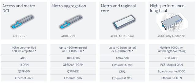
Infinera's XR optics pluggable plans

Infinera’s coherent pluggables for XR optics will also address the company’s metro needs.
Coherent pluggables now dominate the metro market where embedded designs account for just a fifth of all ports, says Infinera.
“As we grow our metro business, we need our own pluggables if we want to be cost-competitive,” says Robert Shore, senior vice president of marketing at Infinera.
Infinera’s family of pluggables implementing the XR optics concept is dubbed ICE-XR.
XR optics splits a coherent optical signal into Nyquist sub-carriers, each carrying a data payload. Twenty-five gigabits will likely be the sub-carrier capacity chosen.
XR optics can be used for point-to-point links where all the sub-carriers go to the same destination. But the sub-carriers can also be steered to different destinations, similar to how breakout cables are used in the data centre.
With XR optics, a module can talk to several lower-speed ones in a point-to-multipoint arrangement. This enables optical feeds to be summed, ideal for traffic aggregation applications such as access and 5G.
Open XR Forum
Infinera detailed its ICE-XR pluggables during the OFC virtual conference and exhibition.
The event coincided with the launch of the Open XR Forum whose members include network operators, Verizon, Lumen Technologies (formerly CenturyLink), Windstream and Liberty Global.
Members of the Open XR Forum span sub-component makers, systems vendors like Infinera, and network operators. The day the Open XR Forum website was launched, Infinera received a dozen enquiries from interested parties.
The Open XR Forum will define standards for XR optics such as how the networks are managed, the form factors used, their speeds and power requirements.
“There are a lot of underlying operational aspects that need to be worked out,” says Shore.
XR optics will use a similar model to ZR+ coherent optics. ZR+ delivers enhanced transmission performance compared to the OIF’s 400ZR coherent standard. “ZR+ is not a standard but rather a set of open specifications that can be used by anyone to create a product, and that is exactly the approach we are taking with XR optics,” says Shore.
Over the last 18 months, Infinera has met with 150 network operators regarding XR optics. “We wanted to validate this is a worthwhile technology and that people wanted it,” says Shore.
There have also been 40 network operator trials of the technology by the end of July. BT has used the technology as part of a metro aggregation trial while Virgin Media and American Tower each tested XR optics over PON.
More members have joined the Open XR Forum and will be announced in the autumn.
ICE-XR
ICE-XR’s name combines two concepts.
The first, ICE, refers to the Infinite Capacity Engine, the optics and coherent digital signal processor (DSP) that is the basis for Infinera’s ICE4 and newer ICE6 coherent transmission designs. ICE4 was Infinera’s first product to use Nyquist sub-carriers.
“XR”, meanwhile, borrows from 400ZR. Here, the ‘X’ highlights that XR supports point-to-point coherent communications, like 400ZR, and point-to-multipoint.
“ICE-XR’s release will be timed in conjunction with the official ratification of the specifications from the Open XR Forum,” says Shore.
Infinera’s ICE-XR portfolio will include 100, 400, and 800-gigabit optical modules.
The 100-gigabit ICE-XR, based on four 25-gigabit sub-carriers, will be offered as QSFP-28, QSDP-DD and CFP2 form factors. The 400-gigabit and 800-gigabit variants, using 16 and 32 sub-carriers respectively, will be available as QSFP-DD and CFP2 modules.
The 100-gigabit and 400-gigabit ICE-XR modules will be released first in 2022.
The 400-gigabit ICE-XR will also double as Infinera’s ZR+ offering when used point-to-point.
Shore says its first ZR+ module will not support the oFEC forward-error correction (FEC) used by the OpenZR+ multi-source agreement (MSA).
“The performance hit you take to ensure multi-vendor interoperability is vastly outweighed by the benefits of the improved [optical] performance [using a proprietary FEC],” says Shore.
Merchant DSP suppliers and the systems vendors with in-house DSP designs all support proprietary FEC schemes that deliver far better performance than oFEC, says Shore.
Infinera is developing a monolithic photonic integrated circuit (PIC) for ICE-XR manufactured at its indium phosphide facility.“ICE-XR will increase the utilisation of our fabrication centre, especially when pluggables produce higher volumes compared to embedded [coherent designs],” says Shore.
Infinera says more than one coherent DSP will be needed for the ICE-XR product portfolio. The modules used have a range of power profiles. The QSFP-28 module will need to operate within 4-5W, for example, while the QSFP-DD implementing ZR+ will need to be below 20W. Developing one DSP to span such a power range is not possible.
Business model
The Open XR Forum’s specifications will enable vendors to develop their own XR optics implementations.
Infinera will also license aspects of its design including its coherent DSPs. The aim, says Shore, is to develop as broad an ecosystem as possible: “We want to make XR optics an industry movement.”
Shore stresses ZR+ interoperability is not a must for most applications. Typically, a vendor’s module will be used at both ends of a link to benefit from the ZR+’s custom features. But interoperability is a must for XR optics given its multi-rate nature. The different speed modules from different vendors must talk to each other.
“Because you have multi-generational and multi-rate designs, it becomes even more important to support multi-vendor interoperability,” says Shore. “It gives the network operators more choice, freedom and flexibility.”
XR optics for the data centre
Infinera says there are developments to use XR optics within the data centre.
As data rates between equipment rise, direct-detect optics will struggle to cope, says Shore. The hierarchical architectures used in data centres also lend themselves to a hub-and-spoke architecture of XR optics.
“This type of technology could fit very nicely into that environment once the capacity requirements get high enough,” says Shore.
For this to happen, power-efficient coherent designs are required. But first, XR optics will need to become established and demonstrate a compelling advantage in a point-to-multipoint configuration.
XR optics will also need to replace traditional direct-detect pluggables that continue to progress; 800-gigabit designs are appearing and 1.6-terabit designs were discussed at OFC. Co-packaged optics is another competing technology.
“You are not looking at the 2022-23 timeframe, but maybe 2025-26,” says Shore.
Covid-era shows
Infinera postponed its customer meetings that pre-covid would take place at OFC till after the show to avoid clashing with the online sessions. Once the meetings occurred, customers were given a tour of Infinera’s virtual OFC booth.
Infinera’s solutions marketing team also divided between them the OFC sessions of interest to attend. The team then ‘met’ daily to share their learnings.
“I do think that the world of in-person events has changed forever,” says Shore. Infinera attended 40 events in 2019. “We will probably do fewer than 20 [a year] going forward,” says Shore.

Nokia adds 400G coherent modules across its platforms

Nokia is now shipping its 400-gigabit coherent multi-haul CFP2-DCO. The module exceeds the optical performance of 400ZR and ZR+ coherent pluggables.
Nokia’s CFP2-DCO product follows its acquisition of silicon photonics specialist, Elenion Technologies, in 2020.
Nokia has combined Elenion’s coherent optical modulator and receiver with its low-power 64-gigabaud (GBd) PSE-Vc coherent digital signal processor (DSP).
Nokia is also adding coherent pluggables across its platform portfolio.
“Not just optical transport and transponder platforms but also our IP routing portfolio as well,” says Serge Melle, director of product marketing, IP-optical networking at Nokia.
“This [amplifier and filter] allows for much better optical performance,”
“This [amplifier and filter] allows for much better optical performance,”
Melle is an optical networking industry veteran. He joined Nokia two years ago after a 15-year career at Infinera. Melle started at Pirelli in 1995 when it was developing a 4×2.5-gigabit wavelength-division multiplexing (WDM) system. In between Pirelli and Infinera, Melle was at Nortel Networks during the optical boom.
400ZR, ZR+ and the multi-haul CFP2-DCO
The CFP2-DCO’s optical performance exceeds that of the QSFP-DD and OSFP form factors implementing 400ZR and ZR+ but is inferior to line-card coherent transponders used for the most demanding optical transport applications.
The 400ZR coherent OIF standard transmits a 400-gigabit wavelength up to 120km linking equipment across data centres. Being a standard, 400ZR modules are interoperable.
The ZR+ adds additional transmission speeds – 100, 200 and 300-gigabits – and has a greater reach than ZR. ZR+ is not a standard but there is the OpenZR+ multi-source agreement (MSA).
Implementing 400ZR and ZR+ coherent modules in a QSFP-DD or OSFP module means they can be inserted in client-side optics’ ports on switches and routers.
The OIF did not specify a form factor as part of the 400ZR standard, says Melle, with the industry choosing the QSFP-DD and OSFP. But with the modules’ limited power dissipation, certain modes of the coherent DSP are turned off, curtailing the feature set and the reach compared to a CFP2-DCO module.
The modules also have physical size restrictions.
“You don’t have enough thermal budget to put an optical amplifier inside the QSFP-DD package,” says Melle. “So you are left with whatever power the DWDM laser outputs through the modulator.” This is -7dBm to -10dBm for 400ZR and ZR+ optics, he says.
The CFP2-DCO is larger such that the DSP modes of encryption, OTN client encapsulation, LLDP snooping (used to gather data about attached equipment), and remote network monitoring (RMON) can be enabled.
The CFP2-DCO can also house an optical amplifier and tunable filter. The filter reduces the out-of-band optical signal-to-noise ratio (OSNR) thereby increasing the module’s sensitivity. “This [amplifier and filter] allows for much better optical performance,” says Melle. A 400-gigabit multi-haul module has a 0dBm optical output power, typically.
The different transceiver types are shown in the table.
Nokia’s paper at the recent OFC virtual conference and exhibition detailed how its 400-gigabit multi-haul CFP2-DCO achieved a reach of 1,200km.
The paper details the transmission of 52, 400-gigabit signals, each occupying a 75GHz channel, for a total capacity of 20.8 terabits-per-second (Tbps).
Melle stresses that the demonstration was more a lab set-up than a live network where a signal goes through multiple reconfigurable optical add-drop multiplexers (ROADMs) and where amplifier stages may not be equally spaced.
That said, the CFP2-DCO’s reach in such networks is 750km, says Nokia.
IP-optical integration
Having coherent pluggables enables 400 Gigabit Ethernet (400GbE) payloads to be sent between routers over a wide area network, says Nokia.
“Given this convergence in form factor, with the QSFP-DD and ZR/ ZR+, you can now do IP-optical integration, putting coherent optics on the router without sacrificing port density or having locked-in ports,” says Melle.
Nokia is upgrading its IP and optical portfolio with coherent pluggables.
“In the routers, ZR/ ZR+, and in transponders not only the high-performance coherent optics – the [Nokia] PSE-Vs [DSP] – but also the CFP2-DCO multi-haul,” says Melle. “The 400-gigabit multi-haul is also going to be supported in our routers.”
Accordingly, Nokia has developed two sets of input-output (I/O) router cards: one supporting QSFP-DDs suited for metro-access applications, and the second using CFP2-DCO ports for metro and regional networks.
The choice of cards adds flexibility for network operators; they no longer need to have fixed CFP2-DCO slots on their router faceplates, whether they are used or not. But being physically larger, there are fewer CFP2-DCO ports than QSFP-DD ports on the I/O cards.
While the QSFP-DD MSA initially defined the module with a maximum power dissipation of 14.5W, a coherent QSFP-DD module consumes 18-20W. Dissipating the heat generated by the modules is a challenge.
Nokia’s airflow cooling is simplified by placing a module on both sides of the line card rather than stacking two CFP2-DCOs, one on top of the other.
Nokia is adding its CFP2-DCO to its 1830 optical transport portfolio. These include its PSI-M compact modular systems, the PSS transponder systems and also its PSS-x OTN switching systems.
The 400ZR/ZR+ module will be introduced with all its routing platforms this summer – the 7250 IXR, 7750 SR, 7750 SR-s, and the 7950 XRS, whereas the CFP2-DCO will be added to its 7750 and 7950 series later this year.
Nokia will source the 400ZR/ZR+ from third parties as well as from its optical networks division.
Its routers use QSFP-DD form-factor for all 400GbE ports and this is consistent for most router vendors in the industry. “Thus, our use and supply of 400ZR/ZR+ pluggable DCOs will focus on the QSFP-DD form-factor,” says Melle. However, the company says it can offer the OSFP form-factor depending on demand.
Network planning study
Nokia published a paper at OFC on the ideal coherent solution for different applications.
For metro aggregation rings with 4-5 nodes and several ROADM pass-throughs, using ZR+ modules is sufficient. Moreover, using the ZR+ avoids any loss in router port density.
For metro-regional core applications, the ZR+’s optical performance is mostly insufficient. Here, the full 400-gigabit rate can not be used but rather 300 gigabit-per-second (Gbps) or even 200Gbps to meet the reach requirements.
Using a 400-gigabit multi-haul pluggable on a router might not match the density of the QSFP-DD but it enables a full 400-gigabit line rate.
For long-haul, the CFP2-DCO’s performance is “reasonable”, says Nokia, and this is where high-performance transponders are used.
What the OFC paper argues is that there is no one-size-fits-all solution, says Melle.
800-Gigabit coherent pluggables
Traditionally, the IEEE has defined short-reach client-side optics while the OIF defines coherent standards.
“If we want this IP-optical convergence continuing in the next generation of optics, those two worlds are going to have to collaborate more closely,” says Melle.
That’s because when a form-factor MSA will be defined, it will need to accommodate the short-reach requirements and the coherent optics. If this doesn’t happen, says Melle, there is a risk of a new split occuring around the IP and optical worlds.
The next generation of coherent pluggables will also be challenging.
All the vendors got together in 2019 and said that 400ZR was just around the corner yet the modules are only appearing now, says Melle.
The next jump in pluggable coherent optics will use a symbol rate of 90-130GBd.
“That is very much the cutting-edge so it brings back the optics as a critical enabling technology, and not just optics but the packaging,” concludes Melle.

II-VI expands its 400G and 800G transceiver portfolio

II-VI has showcased its latest high-speed optics. The need for such client-side modules is being driven by the emergence of next-generation Ethernet switches in the data centre.
The demonstrations, part of the OFC virtual conference and exhibition held last month, featured two 800-gigabit and two 400-gigabit optical transceivers.
“We have seen the mushrooming of a lot of datacom transceiver companies, primarily from China, and some have grown pretty big,” says Sanjai Parthasarathi, chief marketing officer at II-VI.
But a key enabler for next-generation modules is the laser. “Very few companies have these leading laser platforms – whether indium phosphide or gallium arsenide, we have all of that,” says Parthasarathi.
During OFC, II-VI also announced the sampling of a 100-gigabit directly modulated laser (DML) and detailed an optical channel monitoring platform.
“We have combined the optical channel monitoring – the channel presence monitoring, the channel performance monitoring – and the OTDR into a single integrated subsystem, essentially a disaggregated monitoring system,” says Parthasarathi.
An optical time-domain reflectometer (OTDR) is used to characterise fibre.
High-speed client-side transceivers
II-VI demonstrated two 800-gigabit datacom products.
One is an OSFP form factor implementing 800-gigabit DR8 (800G-DR8) and the other is a QSFP-DD800 module with dual 400-gigabit FR4s (2x400G-FR4). The DR8 uses eight fibres in each direction, each carrying a 100-gigabit signal. The QSFP-DD800 supports two FR4s, each carrying four, 100-gigabit wavelengths over single-mode fibre.

“These are standard IEEE-compliant reaches: 500m for the DR8 and 2km for the dual FR4 talking to individual FR4s,” says Vipul Bhatt, senior strategic marketing director, datacom at II-VI.
The 800G-DR8 module can be used as an 800-gigabit link or, when broken out, as two 400-gigabit DR4s or eight individual 100-gigabit DR optics.
II-VI chose to implement these two 800-gigabit interfaces based on the large-scale data centre players’ requirements. The latest switches use 25.6-terabit Ethernet chips that have 100-gigabit electrical interfaces while next-generation 51.2-terabit ICs are not far off. “Our optics is just keeping in phase with that rollout,” says Bhatt.
During OFC, II-VI also showcased two 400-gigabit QSFP112 modules: a 400-gigabit FR4 (400G-FR4) and a multi-mode 400-gigabit SR4 (400G-SR4).
The SR4 consumes less power, is more cost-effective but has a shorter reach. “Not all large volume deployments of data centres are necessarily in huge campuses,” says Bhatt.
II-VI demonstrated its 800-gigabit dual FR4 module talking to two of its QSFP112 400-gigabit FR4s.
Bhatt says the IEEE 802.3db standard has two 400G-SR4 variants, one with a 50m reach and the second, a 100m reach. “We chose to demonstrate 100m because it is inclusive of the 50m capability,” says Bhatt.

II-VI stresses its breadth in supporting multi-mode, short-reach single-mode and medium-reach single-mode technologies.
The company says it was the electrical interface rather than the optics that was more challenging in developing its latest 400- and 800-gigabit modules.
The company has 100-gigabit multi-mode VCSELs, single-mode lasers, and optical assembly and packaging. “It was the maturity of the electrical interface [that was the challenge], for which we depend on other sources,” says Bhatt.
100-gigabit PAM-4 DML
II-VI revealed it is sampling a 100-gigabit PAM-4 directly modulated laser (DML).
Traditionally, client-side modules for the data centre come to market using a higher performance indium phosphide externally-modulated laser (EML). The EML may even undergo a design iteration before a same-speed indium phosphide DML emerges. The DML has simpler drive and control circuitry, is cheaper and has a lower power consumption.
“But as we go to higher speeds, I suspect we are going to see both [laser types] coexist, depending on the customer’s choice of worst-case dispersion and power tolerance,” says Bhatt. It is too early to say how the DML will rank with the various worst-case test specifications.
Parthasarathi adds that II-VI is developing 100-gigabit and 200-gigabit-per-lane laser designs. Indeed, the company had an OFC post-deadline paper detailing work on a 200-gigabit PAM-4 DML.
Optical monitoring system
Optical channel monitoring is commonly embedded in systems while coherent transceivers also provide performance metrics on the status of the optical network. So why has II-VI developed a standalone optical monitoring platform?
What optical channel monitors and coherent modules don’t reveal is when a connector is going bad or fibre is getting bent, says Parthasarathi: “The health and the integrity of the fibre plant, there are so many things that affect a transmission.”
Operators may have monitoring infrastructure in place but not necessarily the monitoring of the signal integrity or the physical infrastructure. “If you have an existing network, this is a very easy way to add a monitoring capability,” says Parthasarathi.

“As we can control all the parts – the optical channel monitoring and the OTDR – we can configure it [the platform] to meet the application,” adds Sara Gabba, manager, analysis, intelligence & strategic marcom at II-VI. “Coherent indeed provides a lot of information, but this kind of unit is also suitable for access network applications.”
The optical monitoring system features an optical switch so it can cycle and monitor up to 48 ports.
With operators adopting disaggregated designs, each element in the optical network is required to have more intelligence and more autonomy.
“If you can provide this kind of intelligent monitoring and provide information about a specific link, you create the possibility to be more flexible,” says Gabba.
Using the monitoring platform, intelligence can be more widely distributed in the optical network complementing systems operators may have already deployed, she adds.

Marvell's first Inphi chips following its acquisition

Marvell unveiled three new devices at the recent OFC virtual conference and show.
One chip is its latest coherent digital signal processor (DSP), dubbed Deneb. The other two chips, for use within the data centre, are a PAM-4 (4-level pulse-amplitude modulation) DSP, and a 1.6-terabit Ethernet physical layer device (PHY).
The chips are Marvell’s first announced Inphi products since it acquired the company in April. Inphi’s acquisition adds $0.7 billion to Marvell’s $3 billion annual revenues while the more than 1,000 staff brings the total number of employees to 6,000.
Marvell spends 30 per cent of its revenues on R&D.
Acquisitions
Inphi is the latest of a series of Marvell acquisitions as it focusses on data infrastructure.
Marvell acquired two custom ASIC companies in 2019: Avera Semiconductor, originally the ASIC group of IBM Microelectronics, and Aquantia that has multi-gigabit PHY expertise.
A year earlier Marvell acquired processing and security chip player, Cavium Networks. Cavium had acquired storage specialist, QLogic, in 2017.
These acquisitions have more than doubled Marvell’s staff. Inphi brings electro-optics expertise for the data centre and optical transport and helps Marvell address the cloud and on-premises data centre markets as well as the 5G carrier market.
Marvell is also targeting the enterprise/ campus market and what it highlights as a growth area, automotive. Nigel Alvares, vice president of solutions at Marvell, notes the growing importance of in-vehicle networking, what he calls a ‘data-centre-on-wheels’.
“Inphi’s technology could also help us in automotive as optical technologies are used for self-driving initiatives in future,” says Alvares.
Inphi also brings integration, co-packaging and multi-chip module expertise.

Merchant chip and custom ASIC offerings
Cloud operators and 5G equipment vendors are increasingly developing custom chip designs. Marvell says it is combining its portfolio with their intellectual property (IP) to develop and build custom ICs.
Accordingly, in addition to its merchant chips such as the three OFC-announced devices, Marvell partners with cloud players or 5G vendors, providing them with key IP blocks that are integrated with their custom IP. Marvell can also build the ASICs.
Another chip-design business model Marvell offers is the integration of different hardware in a multi-chip package. The components include a custom ASIC, merchant silicon, high-speed memory and third-party chiplets.
“We co-package and deliver it to a cloud hyperscaler or a 5G technical company,” says Alvares.
Marvell says this chip strategy serves two market sectors: the cloud hyperscalers and the telcos.
Cloud players are developing custom solutions as they become more vertically integrated. They also have deep pockets. But they can’t do everything because they are not chip experts so they partner with companies like Marvell.
“The five to 10 hyperscalers in the world, they are doing so much creative stuff to optimise applications that they need custom silicon,” says Alvares.
The telcos, in contrast, are struggling to grow their revenues and favour merchant ICs, given they no longer have the R&D budgets of the past. It is this split in the marketplace which Marvell is targeting its various chip services.
OFC announcements
At OFC, Marvell announced the Deneb coherent DSP, used for optical transport including the linking of equipment between data centres.
The Deneb DSP is designed with open standards in mind and complements the 400-gigabit CMOS Canopus DSP announced by Inphi in 2019.
Deneb adds the oFEC forward error correction scheme to support open standards such as OpenZR+, 100-gigabit ZR, the 400-gigabit OpenROADM MSA and CableLabs’ 100-gigabit standard.
The 100-gigabit ZR is targeted at the 5G access market and mobile backhaul. Like the OIF 400G ZR, it supports reaches of 80-120km but uses quadrature phase-shift keying (QPSK) modulation.
“Not only do we support 100 gigabit [coherent] but we also have added the full industrial temperature range, from -40oC to 85oC,” says Michael Furlong, associated vice president, product marketing at Marvell.
The Deneb DSP is sampling now. Both the Deneb and Canopus DSPs will have a role in the marketplace, says Furlong.

Atlas PAM-4 DSP and the 1.6-terabit PHY
Marvell also announced at OFC the Atlas PAM-4 DSP and a dual 800-gigabit PHY devices used within the data centre.
Atlas advances Marvell’s existing family of Polaris PAM-4 DSPs in that it integrates physical media devices. “We are integrating [in CMOS] the trans-impedance amplifier (TIA) and laser drivers,” says Alvares.
Using the 200-gigabit Atlas reduces an optical module design from three chips to two; the Atlas comprises a transmit chip and a receiver chip (see diagram below). Using the Atlas chips reduces the module’s bill of materials, while power consumption is reduced by a quarter.

The Atlas chips, now sampling, are not packaged but offered as bare die and will be used for 200-gigabit SR4 and FR4 modules. Meanwhile, Marvell’s 1.6-terabit PHY – the 88X93160, – is a dual 800-gigabit copper DSP that performs retimer and gearbox functions.
“We view this as the key data centre building block for the next decade,” says Alvares. “The world is just starting to design 100-gigabit serial for their infrastructure.”
The device, supporting 16, 100-gigabit lanes, is the industry’s first 100-gigabit serial retimer, says Marvell. The device drives copper cable and backplanes and is being adopted for links between the server and the top-of-tack switch or to connect switches in the data centre.
The device is suitable for next-generation 400-gigabit and 800-gigabit Ethernet links that use 100-gigabit electrical serialisers-deserialisers (serdes).
The 5nm CMOS device supports over a 38dB (decibel) link budget and reduces I/O power by 40 per cent compared to a 50-gigabit Nigel PAM4-based PHY.
The 100-gigabit serdes design will also be used with Marvell’s Prestera switch portfolio.

Lumentum ships a 400G CFP2-DCO coherent module

Lumentum has started supplying customers with its CFP2-DCO coherent optical module. Operators use the pluggable to add an optical transport capability to equipment.
The company describes the CFP2-DCO as a workhorse; a multi-purpose pluggable for interface requirements ranging from connecting equipment in separate data centres to long-haul optical transmission. The module works at 100-, 200-, 300- and 400-gigabit line rates.
The pluggable also complies with the OpenROADM multi-source agreement. It thus supports the open Forward Error Correction (oFEC) standard, enabling interoperability with oFEC-compliant coherent modules from other vendors.
“We are encountering a fundamental limit set by mother nature around spectral efficiency,”
“Optical communications is getting more diverse and dynamic with the inclusion of the internet content providers (ICPs) alongside traditional telecom operators,” says Brandon Collings, CTO at Lumentum.
The CFP2-DCO module is being adopted by traditional network equipment makers and by the ICPs who favour more open networking.
CFP2-DCOs modules from vendors support the OIF’s 400ZR standard that links switching and routing equipment in data centres up to 120km apart and more demanding custom optical transmission performance requirements, referred to as ZR+.
So what differentiates Lumentum’s CFP2-DCO from other coherent module makers?
Kevin Affolter, Lumentum’s vice president, strategic marketing for transmission, highlights the company’s experience in making coherent modules using the CFP form factor. Lumentum also makes the indium phosphide optical components used for its modules.
“We are by far the leading vendor of CFP2-ACO modules and that will go on for several years yet,” says Affolter.
Unlike the CFP2-DCO that integrates the optics and the digital signal processor (DSP), the earlier generation CFP2-ACO module includes optics only, with the coherent DSP residing on the line card.
The company also offers a 200-gigabit CFP2-DCO that has been shipping for over 18 months.
As a multi-purpose design, Affolter says some customers want to use the CFP2-DCO primarily at 200 gigabits for its long-haul reach while others want the improved performance of the proprietary 400-gigabit mode and its support of Ethernet and OTN clients.
“Each of the [merchant] DSPs has subtly different features,” says Affolter. “Some of those features are important to protect applications, especially for some of the hyperscalers’ applications.”
Higher baud rates
Lumentum did not make any announcements at the recent OFC virtual conference and show regarding indium phosphide-based coherent components operating at the next symbol rate of 128 gigabaud (GBd). But Collings says work continues in its lab: “This is a direction we are all headed.”
The latest coherent optical components operate at 100GBd, making possible 800-gigabit-per-wavelength transmissions. Moving to a 128GBd symbol rate enables a greater reach for the given transmission speed as well as the prospect of 1.2+ terabit wavelengths.
This means fewer coherent modules are needed to send a given traffic capacity, saving costs. But moving to a higher baud rate does not improve overall spectral density since a higher baud rate signal requires a wider channel.
“We are encountering a fundamental limit set by mother nature around spectral efficiency,” says Collings.
Optical transmission technology continues to follow the familiar formula where the more challenging high-end, high-performance coherent systems start as a line-card technology and then, as it matures, transitions to a more compact pluggable format. This trend will continue, says Collings.
The industry goal remains to scale capacity and reduce the dollars-per-bit cost and that applies to high-end line cards and pluggables. This will be achieved using greater integration and increasing the current baud rate.
“Getting capacity up, driving dollars-per-bit down is now what the game is going to be about for a while,” says Collings.
Whether the industry will go significantly above 128GBd such as 256GBd remains to be seen as this is seen as a technically highly challenging task.
However, the industry continues to demand higher network capacity and lower cost-per-bit. So Collings sees a couple of possible approaches to continue satisfying this demand.
The first is to keep driving down the cost of the 128GBd generations of transceivers, satisfying lower cost-per-bit and expanding capacity by using more and more transceivers.
The second approach is to develop transceivers that integrate multiple optical carriers into a single ‘channel’. A channel here refers to a unit of optical spectrum managed through the ROADM network. This would increase capacity per transceiver and lower the cost-per-bit.
“Both approaches are technical and implementation challenges and it remains to be seen which, or both, will be realised across the industry,” says Collings.
100-gigabit PAM-4 directly modulated laser
At OFC Lumentum announced that its 100-gigabit PAM-4 directly modulated laser (DML), which is being used for 500m applications, now supports the 2km-reach FR single-channel and FR4 four-channel client-side module standards.
This is a normal progression of client-side modules for the data centre where the higher performance externally-modulated laser (EML) for a datacom transceiver is the one paving the way. As the technology matures, the EML is replaced by a DML which is cheaper and has simpler drive and control circuitry.
“We started this [trait] with the -LR4 which was dominated by EMLs,” says Mike Staskus, vice president, product line management, datacom at Lumentum. “The fundamental cost savings of a DML is its smaller chip size, more chips per wafer, and fewer processes, fewer regrowths.”
The company is working on a 200-gigabit EML and a next-generation 100-gigabit DML that promises to be lower cost and possibly uncooled.
Reconfigurable optical add-drop multiplexers (ROADMs)
Lumentum is working to expand its wavelength-selective switches (WSSes) to support the extended C-band, and C- and L-band options as a way to increase transmission capacity.
“We are expanding the overall ROADM portfolio to accommodate extended C-band and more efficient C-band and L-band opportunities to continue to build capacity into ROADM networks,” says Collings. “As spectral efficiency saturation sets in, we are going to need more amplified bandwidth and more fibres, and the C- and L-bands will double fibre capacity.”
The work includes colourless and directionless; colourless, directionless and contentionless, and higher-degree ROADM designs.
Intel details its 800-gigabit DR8 optical module

The company earmarks 2023 for its first co-packaged optics product
Intel is sampling an 800-gigabit DR8 in an OSFP pluggable optical module, as announced at the recent OFC virtual conference and show.
“It is the first time we have done a pluggable module with 100-gigabit electrical serdes [serialisers/ deserialisers],” says Robert Blum, Intel’s senior director, marketing and new business. “The transition for the industry to 100-gigabit serdes is a big step.”
The 800-gigabit DR8 module has eight electrical 100-gigabit interfaces and eight single-mode 100-gigabit optical channels in each transmission direction.
Intel demonstrated a prototype 12.8-terabit co-packaged optics design
The attraction of the single-module DR8 design, says Blum, is that it effectively comprises two 400-gigabit DR4 modules. “The optical interface allows you the flexibility that you can break it out into 400-gigabit DR4,” says Blum. “You can also do single 100-gigabit breakouts or you can do 800-gigabit-to-800-gigabit traffic.”
Intel expects volume production of the DR8 in early 2022. Developing a DR8 in a QSFP-DD800 form factor will depend on customer demand, says Blum.
Intel will follow the 800-gigabit DR8 module with a dual 400G FR4, expected later in 2022. The company is also developing a 400-gigabit FR4 module that is expected then.
Meanwhile, Intel is ramping its 200-gigabit FR4 and 400-gigabit DR4 modules.
51.2-terabit co-packaged optics
Intel demonstrated a prototype 12.8-terabit co-packaged optics design, where the optics is integrated alongside its Tofino 2 Ethernet switch chip, at last year’s OFC event.
The company says its first co-packaged optics design will be for 51.2-terabit switches and is scheduled in late 2023. “We see smaller-scale deployments at 51.2 terabits,” says Blum.
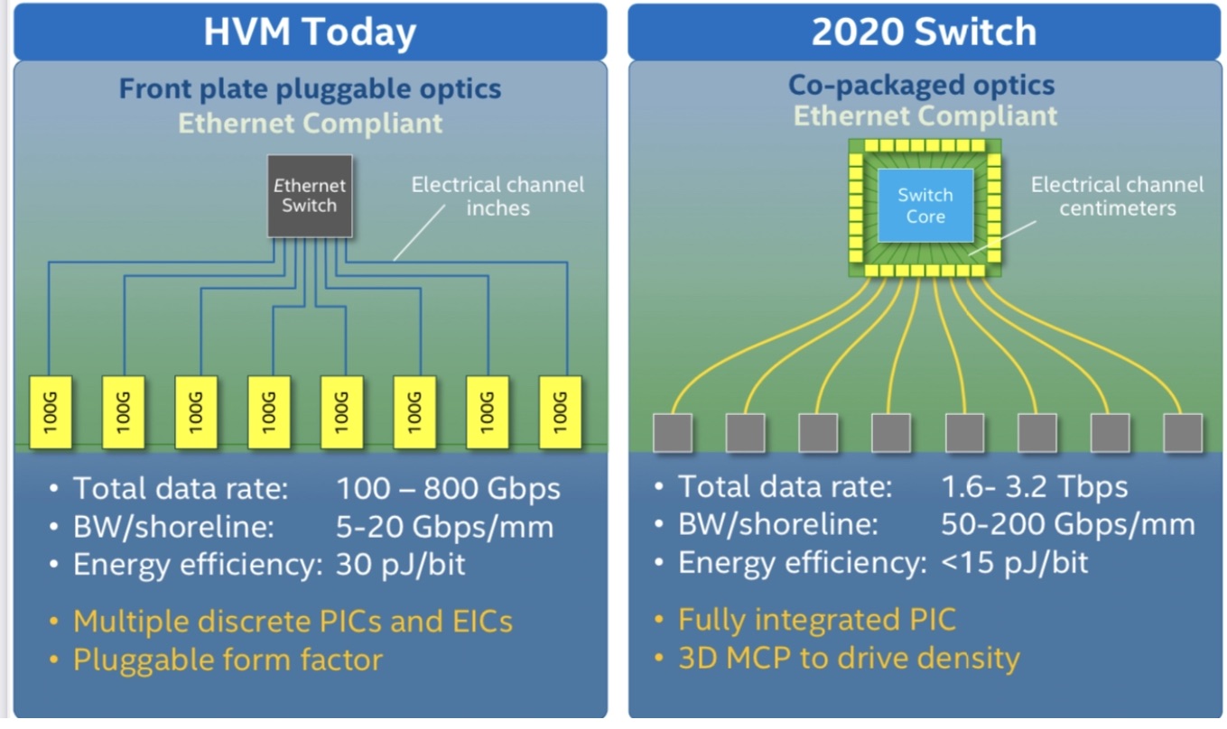
Moving the industry from pluggable optical modules to co-packaged optics is a big shift, says Intel. The technology brings clear system benefits such as 30 per cent power savings and lower cost but these must be balanced against the established benefits of using pluggable modules and the need to create industry partnerships for the production of co-packaged optics.
The emergence of 800-gigabit client-side pluggable modules such as Intel’s also means a lesser urgency for co-packaged optics. “You have something that works even if it is more expensive,” says Blum.
Thirty-two 800-gigabit modules can serve a 25.6-terabit switch in a one rack unit (1RU) platform.
However, for Intel, the crossover point occurs once 102.4-terabit switch chips and 200-gigabit electrical interfaces emerge.
“We see co-packaged optics as ubiquitous; we think pluggables will no longer make sense at that point,” says Blum.
FPGA-based optical input-output
Intel published a paper at OFC 2021 highlighting its latest work a part of the U.S. DARPA PIPES programme.
The paper describes a co-packaged optics design that adds 8 terabits of optical input-output (I/0) to its Stratix 10 FPGA. The design uses Ayar Labs’ TeraPHY chiplet for the optical I/O.
The concept is to use optical I/O to connect compute nodes – in this case, FPGAs – that may be 10s or 100s of meters apart.
Intel detailed its first Stratix 10 with co-packaged optical I/O two years ago.
The latest multi-chip package also uses a Stratix 10 FPGA with Intel’s Advanced Interface Bus (AIB), a parallel electrical interface technology, as well as the Embedded Multi-die Interconnect Bridge (EMIB) technology which supports the dense I/O needed to interface the FPGA to the TeraPHY chiplet. The latest design integrates five TeraPHYs compared to the original one that used two. Each chiplet offers 1.6 terabits of capacity such that the FPGA-based co-package has 8 terabits of I/O in total.
Optically enabling Ethernet silicon or an FPGA is part of the industry’s vision to bring optics close to the silicon. Other devices include CPUs and GPUs and machine-learning devices used in computing clusters that require high-density interconnect (see diagram below).
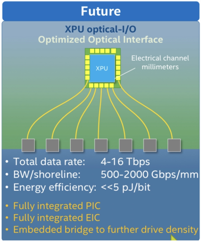
“It is happening first with some of the highest bandwidth Ethernet switches but it is needed with other processors as well,” says Blum.
The Intel OFC 2021 paper concludes that co-packaged optics is inevitable.
Milestones, LiDAR and sensing
Intel has shipped a total of over 5 million 100-gigabit optical modules, generating over $1 billion of revenues.
Blum also mentioned Intel’s Mobileye unit which in January announced its LiDAR-on-a-chip design for autonomous vehicles.
“We have more than 6,000 individual components on this LiDAR photonic integrated circuit,” says Blum. The count includes building blocks such as waveguides, taps, and couplers.
“We have this mature [silicon photonics] platform and we are looking at where else it can be applied,” says Blum.
LiDAR is one obvious example: the chip has dozens of coherent receivers on a chip and dozens of semiconductor optical amplifiers that boost the output power into free space. “You really need to integrate the different functionalities for it to make sense,” says Blum.
Intel is also open to partnering with companies developing biosensors for healthcare and for other sensing applications.
Certain sensors use spectroscopy and Intel can provide a multi-wavelength optical source on a chip as well as ring-resonator technology.
“We are not yet at a point where we are a foundry and people can come but we could have a collaboration where they have an idea and we make it for them,” says Blum.

Making optical networking feel like cycling downhill

BT’s chief architect, Neil McRae, is a fervent believer in the internet, a technology built on the continual progress of optical networking. He discussed both topics during his invited talk at the recent OFC 2021 virtual conference and exhibition.
Neil McRae’s advocacy of the internet as an educational tool for individuals from disadvantaged backgrounds stems from his childhood experiences.
“When I was a kid, I lived in a deprived area and the only thing that I could do was go to the library,” says McRae, chief architect and managing director for architecture and technology strategy at BT.
His first thought on discovering the internet was just how much there was to read.
“If I’m honest, everything I’ve learnt in technology has been pretty much self-taught,” says McRae.
This is why he so values the internet. It has given him a career where he has travelled widely and worked with talented and creative people.
“Anyone who is out there in the world can do the same thing,” he says. “I strongly believe that the internet brings opportunities to people who are willing to spend the time to learn.”
Optical networking
McRae surveyed the last 20 years of optical networking in his OFC talk. He chose the period since it was only at the end of the last century that the internet started to have a global impact.
“The investment in networking [during this period] has been orders of magnitude bigger than prior years,” says McRae. “There has also been a lot of deregulation across the world, more telecoms companies, more vendors and ultimately more people getting connected.”
In 2000, networks used the SONET/SDH protocol and fixed wavelengths. “We have brought in many new technologies – coherent, coloured optics, programable lasers and silicon photonics – and they have been responsible for pretty significant changes.”
McRae likens optical network to gears on a bike. “It powers the rest of what we do in the network and without those advances, we wouldn’t be the digitally connected society we are today,” says McRae. “If I think about the pandemic of the last year, can you imagine what the pandemic would have been like if it had happened in the year 2000?”
McRae says he spends a fifth of his time on optical networking. This is more than previously due to the relentless growth in network bandwidth.
“Ultimately, if you get optical wrong, it feels like you are in the wrong gear cycling uphill,” says McRae. “If you get it right, you are in the right gear, you are going as fast as you can go and it feels like a downhill ride.”
And it’s not just bandwidth but also from a cost, capability and customer experience perspective. “We recognise the value that it brings to all the other layers right up to the application,” he says.
Research
BT Labs has an optical networking programme that is run by Professor Andrew Lord. The programme’s remit is to help BT address existing and future issues.
“There is a longer-term research aspect to what Andrew and his team do, but there are some here-and-now issues that they support me on like the hollow-core fibre work and some of the 400-gigabit [coherent] platforms we have been reviewing recently,” he says.
He cites as examples the work the programme did for BT’s next-generation optical platform that was designed for growth and which indeed has grown massively in the last decade. “We have launched optical services as a product because of the platform,” says McRae.
The programme has also helped Openreach, BT Group’s copper and fibre plant subsidiary, with its fibre-to-the-premise (FTTP) deployments that use such technologies as GPON and XGS-PON.
Reliable, dynamic, secure networks
McRae admits he is always nervous about predicting the future. But he is confident 400 gigabits will be a significant optical development over the next decade.
This includes inside the data centre, driven by servers, and in the network including long haul.
“The challenge will be around getting the volume and interoperability as quickly as we possibly can,” says McRae.
The other big opportunity is the increased integration of IP and optical using a control plane aligned to both.
“The biggest networking technology out there is IP,” says McRae. “And that will not change in the coming decade.”
The Layer-3 capabilities include working around issues but it is bad at managing bandwidth. Optical is the opposite: great at managing bandwidth but less dynamic for working around problems. Merging the two promises significant benefits.
This idea, advocated as IP-over-DWDM, has long been spoken of but has not been deployed widely. The advent of 400-gigabit coherent implemented using client-side modules means that the line-side interface density can equal that of the host. And other developments such as software-defined networking and artificial intelligence also help.
Software-defined networking will make a big difference because it will enable the move to automation and that will enable new technologies such as artificial networking (AI) and machine-learning to be introduced.
McRae talks of a control plane capable of deciding which interface to send packets down and also determine what paths to create across the optical infrastructure.
“We have seen some of that but we have not seen enough,” says McRae. AI and machine-learning technologies will provide networks with almost autonomous control over which paths to use and enable for the various traffic types the network sees.
McRae stresses that it is getting harder to get the maximum out of the network: “If we maintain human intervention, the network will never see its full potential because of complexity, demands and scale.”
He predicts that once the human component is taken out of the network, some of the silos between the different layers will be removed. Indeed, he believes networks built by AI and aided by automation will look very different to today’s networks.
Another technology McRae highlights is hollow-core fibre which BT Labs has been researching.
“Increasingly, we are starting to reach some limits although many folks have said that before, but hollow-core fibre gives us some interesting and exciting opportunities around latency and the total use of a fibre,” says McRae.
There are still challenges to be overcome such as manufacturing the fibre at scale but he sees a path in many parts of the network where hollow-core fibre could be valuable to BT.
Quantum key distribution (QKD) and the importance of network security is another area starting to gain momentum.
“We have gone from a world where people were scared to send an email rather than a fax to one where the network is controlling mission-critical use cases,” says McRae. “The more secure and reliable we make those networks, the more it will help us in our everyday lives.”
McRae believes this is the decade where the underlying optical network capability coupled with QKD security will take effect.
Making a difference
McRae has run several events involving children with autism although during the pandemic this has not happened. He uses gaming as a way to demonstrate how electronics works – switching things on and off – and then he introduces the concept of computer programming.
“I find that kids with autism get it really quickly” he says. BT runs such events two or three times a year.
McRae also works with children who are learning to program but find it difficult. “Again, it is something self-taught for me,” he says although he quips that the challenge he has is that he teaches them bad programming habits.
“I’m keen to find the next generation of fantastic engineers; covid has shown us that we need them more than ever,” he says.