
Intel combines optics to its Tofino 2 switch chip
Part 1: Co-packaged Ethernet switch
The advent of co-packaged optics has moved a step closer with Intel’s demonstration of a 12.8-terabit Ethernet switch chip with optical input-output (I/O).
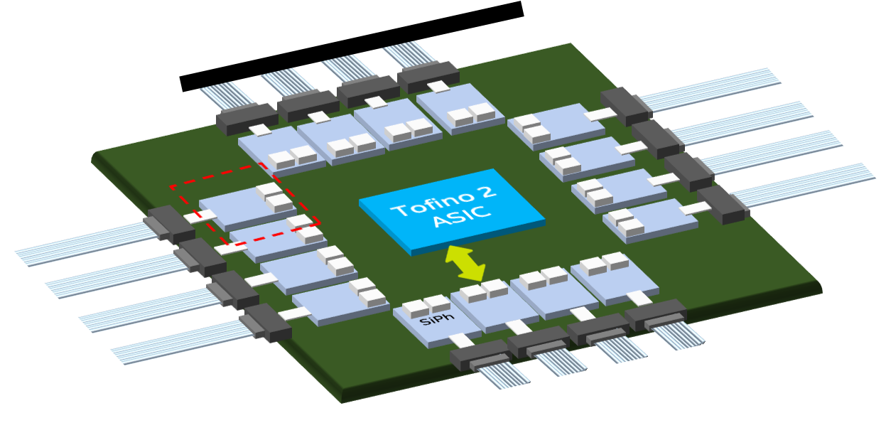
The design couples a Barefoot Tofino 2 switch chip to up to 16 optical ‘tiles’ – each tile, a 1.6-terabit silicon photonics die – for a total I/O of 25.6 terabits.
“It’s an easy upgrade to add our next-generation 25.6-terabit [switch chip] which is coming shortly,” says Ed Doe, Intel’s vice president, connectivity group, general manager, Barefoot division.
Intel acquired switch-chip maker, Barefoot, seven months ago after which it started the co-packaging optics project.
Intel also revealed that it is in the process of qualifying four new optical transceivers – a 400Gbase-DR4, a 200-gigabit FR4, a 100-gigabit FR1 and a 100Gbase-LR4 – to add to its portfolio of 100-gigabit PSM4 and CWDM4 modules.
Urgency
Intel had planned to showcase the working co-packaged switch at the OFC conference and exhibition, held last week in San Diego. But after withdrawing from the show due to the Coronavirus outbreak, Intel has continued to demonstrate the working co-packaged switch at its offices in Santa Clara.

“We have some visionaries of the industry coming through and being very excited, making comments like: ‘This is an important milestone’,” says Hong Hou, corporate vice president, general manager, silicon photonics product division at Intel.
“There are a lot of doubts still [about co-packaged optics], in the reliability, the serviceability, time-to-market, and the right intercept point [when it will be needed]: is it 25-, 51- or 102-terabit switch chips?” says Hou. “But no one says this is not going to happen.”
If the timing for co-packaged optics remains uncertain, why the urgency?
“There has been a lot of doubters as to whether it is possible,” says Doe. “We had to show that this was feasible and more than just a demo.”
Intel has also been accumulating IP from its co-packaging work. Topics include the development of a silicon-photonics ring modulator, ensuring optical stability and signal integrity, 3D packaging, and passive optical alignment. Intel has also developed a fault-tolerant design that adds a spare laser to each tile to ensure continued working should the first laser fail.
“We can diagnose which laser is the source of the problem, and we have a redundant laser for each channel,” says Hou. “So instead of 16 lasers we have 32 functional lasers but, at any one time, only half are used.”
Co-packaged optics
Ethernet switches connected in the data centre currently use pluggable optics. The switch chip resides on a printed circuit board (PCB) and is interfaced to the pluggable modules via electrical traces.
But given that the capacity of the Ethernet switch ICs is doubling every two years, the power consumption of the I/O continues to rise yet the power delivered to a data centre is limited. Accordingly, solutions that ensure a doubling of switch speed but do not increase the power consumed are required.
One option is embedded optics such as the COBO initiative. Here, optics are moved from the switch’s faceplate onto the PCB, closer to the switch chip. This shortens the electrical traces while overcoming the capacity limitations of the number of pluggable modules that can be fitted onto the switch’s faceplate. Freeing up the faceplate by removing pluggables also improves airflow to cool the switch.
The second, more ambitious approach is co-packaged optics where optics are combined with the switch ASIC in the one package.
Co-packaged optics can increase the overall I/O on and off the switch chip, something that embedded optics doesn’t address. And placing the optics next to the ASIC, the drive requirements of the high-speed serialiser-deserialisers (serdes) is simplified.
Meanwhile, pluggable optics continue to advance in the form factors used and their speeds as well as developments such as fly-over cables that lower the loss connecting the switch IC to the front-panel pluggables.
In turn, certain hyperscalers are not convinced about co-packaged optics.
Microsoft and Facebook announced last year the formation of the Co-Packaged Optics (CPO) Collaboration to help guide the industry to develop the elements needed for packaging optics. But Google and Alibaba said at OFC that they prefer the flexibility and ease of maintenance of pluggables.
Data centre trends
The data centre is a key market for Intel which sells high-end server microprocessors, switch ICs, FPGAs and optical transceivers.
Large-scale data centres deploy 100,000 servers, 50,000 switches and over one million optical modules. And a million pluggable modules equate to $150M to $250M of potential revenue, says Intel.

“One item that is understated is the [2:1] ratio of servers to switches,” says Doe. “We have seen a trend in recent years where the layers of switching in data centres have increased significantly.”
One reason for more switching layers is that traffic over-subscription is no longer used. With top-of-rack switches, a 3:1 over-subscription was common which limited the switch’s uplink bandwidth needed.
However, the changing nature of the computational workloads now requires that any server can talk to any other server.
“You can’t afford to have any over-subscription at any layer in the network,” says Doe. “As a result, you need to have a lot more bandwidth: an equal amount of downlink bandwidth to uplink bandwidth.”
Another factor that has increased the data centre’s switch layer count is the replacement of chassis switches with disaggregated pizza boxes. Typically, a chassis switch encompasses three layers of switching.
“Disaggregation is a factor but the big one is the 1:1 [uplink-downlink bandwidth] ratio, not just at the top-of-rack switch but all the way through,” says Doe. “They [the hyperscalers] want to have uniform bandwidth throughout the entire data centre.”
Tofino switch IC
Barefoot has two families of Tofino chips. The first-generation Tofino devices have a switching capacity ranging from 1.2 to 6.4 terabits and are implemented using a 16nm CMOS process. The Tofino 2 devices, implemented using a 7nm CMOS IC, range from 4 terabits to 12.8 terabits.
“What we having coming soon is the Tofino next-generation which will go to both 25 terabits and 51 terabits,” says Doe.
Intel is not discussing future products but Doe hints that both switch ICs will be announced jointly rather than the typical two-year delay between successive generations of switch IC. This also explains the urgency of the company’s co-packaging work.
The 12.8-terabit Tofino 2 chip comprises the switch core dies and four electrical I/O tiles that house the device’s serdes.
“The benefit of the tile design is that it allows us to easily swap the tiles for higher-speed serdes – 112 gigabit-per-second (Gbps) – once they become available,” says Doe. And switching the tiles to optical was already envisaged by Barefoot.
Optical tile
Intel’s 1.6-terabit silicon-photonics tile includes two integrated lasers (active and spare), a ring modulator, an integrated modulator driver, and receiver circuitry. “We also have on-chip a v-groove which allows for passive optical alignment,” says Hou.
Each tile implements the equivalent of four 400GBASE-DR4s. The 500m-reach DR4 comprises four 100-gigabit channels, each sent over single-mode fibre.
“This is a standards-based interface,” says Robert Blum, Intel’s director of strategic marketing and business development, as the switch chip must interact with standard-based optics.
The switch chip and the tiles sit on an interposer. Having an interposer will enable different tiles and different system-on-chips to be used in future.
Hou says that having the laser integrated with the tile saves power. This contrasts with designs where the laser is external to the co-packaged design.
The argument for using an external laser is that it is remote from the switch chip which runs hot. But Hou says that the switch chip itself has efficient thermal management which the tile and its laser(s) can exploit. Each tile consumes 35W, he says.
As for laser reliability, Intel points to its optical modules that it has been selling since 2016 when it started selling the PSM4.
Hou claims Intel’s hybrid laser design, where the gain chip is separated from the cavity, is far more reliable than a III-V facet cavity.
“We have shipped over three million 100-gigabit transceivers, primarily the PSM4. The DPM [defects per million] is 28-30, about two orders of magnitude less than our closest competitor,” says Hou. “Eight out of ten times the cause of the failure of a transceiver is the laser, and nine out of ten times, the laser failure is due to a cavity problem.”
The module’s higher reliability reduces the maintenance needed, and enables data centre operators to offer more stringent service-level agreements, says Hou.
Intel says it will adopt wavelength-division multiplexing (WDM) to enable a 3.2-terabit tile which will be needed with the 51.2-terabit Tofino.
Switch platform
Intel’s 2-rack-unit (2RU) switch platform is a hybrid design: interfaced to the Tofino 2 are four tiles as well as fly-over cables to connect the chip to the front-panel pluggables.
“The hyperscalers are most interested in co-packaging but when you talk to enterprise equipment manufacturers, their customers may not have a fabric as complicated as that of the hyperscalers,” says Hou. “Bringing pluggables in there allows for a transition.”
The interposer design uses vertical plug-in connectors enabling a mix of optical and electrical interfaces “It is pretty easy, at the last minute, to [decide to] bring in 10 optical [interfaces] and six fly-over cables [to connect] to the pluggables,” says Hou.
“This is not like on-board optics,” adds Blum. “This [connector arrangement] is part of the multi-chip package, it doesn’t go through the PCB. It allows us to have [OIF-specified] XSR serdes and get the power savings.”
Intel expects its co-packaged design to deliver a 30 per cent power saving as well as a 25 to 30 per cent cost-saving. And now that it has a working platform, Hou expects more engagements with customers that seeking these benefits and its higher-bandwidth density.
“This can stimulate more discussions and drive an ecosystem formation around this technology,” concludes Hou.
See Part 2: Ranovus outlines its co-packaged optics plans.

Acacia unveils its 400G coherent module portfolio

Acacia Communications has unveiled a full portfolio of 400-gigabit coherent optics and has provided test samples to customers, one being Arista Networks.
Delivering a complete set of modules offers a comprehensive approach to address the next phase of coherent optics, the company says.
The 400-gigabit coherent designs detailed by Acacia are implemented using the QSFP-DD, OSFP and CFP2 pluggable form factors.
Collectively, the pluggables support three performance categories: the 400ZR standard, OpenZR+ that is backed by several companies, and the coherent optics specification used for the Open ROADM multi-source agreement (MSA).
OIF-defined 400ZR standard designed for hyperscalers
“These are challenging specifications,” says Tom Williams, vice president of marketing at Acacia. “Even the 400ZR, where the objective has been to simplify the requirements.”
400ZR and OpenZR+
The OIF-defined 400ZR standard is designed for hyperscalers to enable the connection of switches or routers in data centres up to 120km apart.
The 400ZR standard takes in a 400 Gigabit Ethernet (GbE) client signal and outputs a 400-gigabit coherent signal for optical transmission.
“Hyperscaler customers want a limited subset of performance [with the ZR] because they don’t want to introduce operational complexity,” says Williams.
Acacia is implementing the 400ZR standard with two module offerings: the QSFP-DD and the OSFP.
Acacia is also a founding member of OpenZR+, the industry initiative that supports both 400ZR and extended optical performance modes. The other OpenZR+ members are NEL, Fujitsu Optical Components, Lumentum, Juniper Networks and Cisco Systems which is in the process of acquiring Acacia.
OpenZR+ supports 100GbE and its multiples (200GbE and 300GbE) input signals, not just 400GbE as used for ZR. To transmit the 200- 300- and 400GbE client signals, OpenZR+ uses quadrature phase-shift keying (QPSK), 8-ary quadrature amplitude modulation (8-QAM), and 16-QAM, respectively.
OpenZR+ also employs an enhanced forward-error correction (oFEC) used for the Open ROADM specification and delivers improved dispersion compensation performance.
“OpenZR+ is not just about going further but also being able to offer more functionality than 400ZR,” says Williams.
Acacia is implementing OpenZR+ using the QSFP-DD and OSFP form factors.
Open ROADM
The Open ROADM specification is the most demanding of the three modes and is targeted for use by the telecom operators. Here, a CFP2-DCO module is used due to its greater power envelope. And while the Open ROADM optics is aimed at telcos, the CFP2-DCO also supports OpenZR+ and 400ZR modes.
“The telcos are not as focussed on [face plate] density,” says Williams. “The CFP2-DCO has a higher output and is not limited to just Ethernet but also multiplexed client signals and OTN.”
Since line cards already use CFP2-DCO modules, the Open ROADM module enables a system upgrade. Existing line cards using the 200-gigabit CFP2-DCO may not support 400GbE client signals but with the Open ROADM CFP2’s higher symbol rate, it offers enhanced reach performance.
This is because the Open ROADM CFP2-DCO uses a 64 gigabaud (GBd) symbol rate enabling a 200-gigabit signal to be transmitted using QPSK modulation. In contrast, 32GBd is used for the existing 200-gigabit CFP2-DCOs requiring 16-QAM. Using QPSK rather than 16-QAM enables better signal recovery.
There is also an interoperability advantage to the new CFP2-DCO in that its 200-gigabit mode is compliant with the CableLabs specification.
All three designs – 400ZR, OpenZR+ and Open ROADM – use Acacia’s latest 7nm CMOS Greylock low-power coherent digital signal processor (DSP).
This is the company’s third-generation low-power DSP following on from its Sky and Meru DSPs. The Meru DSP is used in existing 32GBd 100/ 200-gigabit CFP2-DCOs.
3D stacking
Acacia has spent the last year and a half focusing on packaging, using techniques from the semiconductor industry to ensure the pluggable form factors can be made in volume.
The higher baud rate used for the 400-gigabit coherent modules means that the electronic ICs and the optics need to be closely coupled. “Moving up the baud rate means that the interconnection between the [modulator] driver [chip] and the modulator can become a limiting factor,” says Williams.
Acacia is not detailing the 3D design except to say that the Greylock DSP, its silicon-photonics photonic integrated circuit (PIC), and the modulator driver and trans-impedance amplifier (TIA) are all assembled into one package using chip-stacking techniques. The chip is then mounted onto a printed circuit board much like a BGA chip, resulting in a more scalable process, says Acacia.
“We have taken the DSP and optics and turned that into an electronic component,” says Williams. “Ultimately, we believe it will lead to improvements in reliability using this volume-repeatable process.”
Acacia says its modules will undergo qualification during most of this year after which production will ramp.
No one module design will be prioritised, says Williams: “There are a lot of benefits of doing all three, leveraging a lot of common elements.”

The 50th anniversary of light-speed connections at OFC

The 50th anniversary of two key optical developments will be celebrated at the upcoming OFC show to take place in San Diego starting March 8th.
Back in 1970 the first low-loss fibre and the first room-temperature semiconductor laser were demonstrated.
“The low-loss fibre had a loss of 16 decibels-per-kilometre,” says Jun Shan Wey of ZTE and the OFC programme co-chair. “Without such optical fibre, there would be no chance of any long-distance communication.”
The advent of a semiconductor laser operating at room temperature was another development of key importance, she adds.
The Fiber 50 celebrations and recognition of the invention of the first EDFA
Fiber 50 Keynote
The Fiber 50 celebrations include a series of events assessing the impact of the two optical-communication enablers as well as looking to the future.
Dave Welch, founder and chief innovation officer at Infinera, will open the event with a keynote talk (Tuesday, 10 March 2020, 18:15 – 19:00 Ballroom 20BCD) addressing the impact of optical communications on society over the last half-century and discussing what to expect in the coming years.
According to Welch, advances witnessed in the technology are the result of game-changing innovations such as the erbium-doped fibre amplifier (EDFA), “a critical enabler” for dense wavelength-division multiplexing (DWDM).
Professor Sir David Payne, that led the team that invented the EDFA, is one of this year’s OFC Plenary Session speakers.
“What is so striking is how the world has changed as a consequence of the fibre network,” says Welch. “I do not believe that there has been anything more globally impactful than the fibre-optic network because, without it, the internet could not exist.“

Fibre-optic communication has also transformed the business world.
“If we look at the top ten companies as defined by market valuation and compare the list from 1997 to the list today, it is stunning,” says Welch.
Back then it was energy firms and bricks-and-mortar companies whereas today the list is dominated by companies built on data and the communication of that data.
Welch will also highlight in his keynote what to expect going forward.
“What is highly predictable is the continued expansion of bandwidth consumption and the cost of bandwidth continuing to drop,” says Welch.
The technologies that enable the network will also be highly innovative. “For example, optical communication will draw even more from radio network designs, and from the functional convergence of physical layers of the network to achieve continued expansion,” says Welch.
The networks will also be built with machines in mind, not just humans. “This is where most of the traffic expansion is coming from today and in the future,” concludes Welch.
Vision 2030
Welch’s Fiber 50 keynote talk will be followed by a conference reception (Tuesday 10 March 2020, 19:00 – 20:30 Sails Pavilion) where key individuals in the development of optical communications will be present.
The OFC also has a Special Chair’s Session entitled: Vision 2030: Taking Optical Communications through the Next Decade (Wednesday, 11 March 2020, 14:00-18:30 Room: 6F) where industry luminaries will discuss key topic directions over the next decade.
These include data centres; optical devices such as terabit transmitters, indium phosphide photonic integrated circuits (PICs) and silicon/ nanophotonics; undersea communications; optical access, and 5G optical transport.
Wey highlights how new technologies such as machine learning and quantum techniques for optical communications feature widely across this year’s OFC conference sessions.
“My view is that we are seeing a ‘hockey-stick’ of ideas coming in as we enter the next decade,” says Wey.
She cites access networks as an example. In the past decade, the main driver has been increasing access bit rates. This remains important, she says, but other considerations are also driving access.
5G is changing the architectural requirements, not just the increase in bandwidth but in the use cases it will support. Multi-access edge computing is another aspect.
“Cloud and virtualisation are coming into access, and then there is the challenge of how vendors stay in business,” says Wey.
Exhibits
The OFC has also organised a timeline-of-innovation exhibition on the show floor with items being loaned by companies for the event.
The exhibits will include a 1970 lithium niobate modulator, a 1977 fibre prototype from Corning that carried the first commercial traffic, an early fibre-to-the-home BPON optical transceiver and the first coherent optical transmission system from Ciena (Nortel).
Lastly, there will be an interactive exhibit honouring the recipients of The John Tyndall Award. The award is presented by the IEEE and the OSA to 33 individuals that have made outstanding contributions in optical fibre technology.
“We are very excited and proud in what we have put together,” says Wey. The other OFC programme co-chairs are Professor David Plant of McGill University and Shinji Matsuo of NTT.