
Avicena partners with TSMC to make its microLED links
TSMC, the leading semiconductor foundry, will make the photo-detectors used for Avicena Tech’s microLED optical interconnect technology.
Avicena is developing an optical interface that uses hundreds of parallel fibre links – each link comprising a tiny LED tranmitter and a silicon photo-detector receiver – to deliver terabit-per-second (Tbps) data transfers.
Avicena is targeting its microLED-based interconnect, dubbed LightBundle, for artifical intelligence (AI) and high-performance computing (HPC) applications.
The deal is a notable step for Avicena, aligning its technology with TSMC’s CMOS manufacturing prowess. The partnership will enable Avicena to transition its technology from in-house prototyping to high-volume production.
Visible-light technology
Avicena’s interconnects operate in the visible light spectrum at 425-430nm (blue light), differing from the near-infrared used by silicon photonics. The lower wavelength band enables simpler photo-detector designs where silicon efficiently absorbs blue light.
“Silicon is a very good detector material because the absorption length at that kind of wavelength is less than a micron,” says Christoph Pfistner, vice president of sales and marketing at Avicena. “You don’t need any complicated doping with germanium or other materials required for infrared detectors.”
Visible-light detectors can therefore be made using CMOS processes. For advanced CMOS nodes, however, such as used to make AI chips, hybrid bonding is required with a separate photo-detector wafer.
TSMC is adapting its CMOS Image Sensor (CIS) process used for digital cameras that operate in the megahertz range, to support Avicena’s photo-detectors that must work in the gigahertz range.
For the transmitter, Avicena uses gallium nitride-based microLEDs developed for the micro-display industry, paired with CMOS driver chips. Osram is Avicena’s volume LED supplier.
Osram has adapted its LED technology for high-speed communications and TSMC is now doing the same for the photo-detectors, enabling Avicena to mass produce its technology.
Specifications
The LED is used to transmit non-return-to-zero (NRZ) signalling at 3.5 to 4 gigabit-per-second (Gbps). Some 300 lanes are used to send the 800 gigabit data payload, clock, and associated overhead bits.
For the transmitter, a CMOS driver modulates the microLED while the receiver comprises a photo-detector, a trans-impedance amplifier (TIA) and a limiting amplifier.
By operating in this ‘slow and wide’ manner, the power consumption of less than 1 picojoule-per-bit (pJ/b) is achievable across 10m of the multi-mode fibre bundle. This compares to 3-5pJ/b using silicon photonics and up to 20pJ/b for optical pluggable transceivers though the latter support longer reaches.
The microLED links achieve a bandwidth density of over 1 terabit/mm and Avicena says this can be improved. Since the design is a 2D array, it is possible to extend the link density in area (in 2D) and not be confined to the ‘beachfront’ stretch. But this will be within certain limits, qualifies Pfistner
Applications
A key theme at the recent OFC 2025 show was optical interconnect options to linearly scale AI processing performance by adding more accelerator chips, referred to as the scale-up architecture.
At present copper links are used to scale up accelerators but the consensus is that, at some point, optics will be needed once the speed-distance performance of copper is exceeded. Nvidia’s roadmap suggests that copper can still support larger scale-up architectures for at least a couple of graphics processing unit (GPU) generations yet.
Avicena is first targeting its microLED technology in the form of an optical engine to address 1.6Tbps on-board optics modules. The same optical engine can also be used in active optical cables.
The company also plans to use its optical engine for co-packaged optics, and for in-package interconnect applications using a die-to-die (D2D) electrical interface such as the Universal Chiplet Interconnect Express (UCIe) or the OCP’s Bunch of Wires (BOW) interface. On-board optics, also known as co-packaged optics, refers to optics on a separate substrate close to the host ASIC, with both packaged together.
One such application for in-packaged optics is memory disaggregation involving high-bandwidth memory (HBM). “There’s definitely more and more interest in what some people refer to as optical HBM,” says Pfistner. He expects initial deployment of optical HBM in the 2029-2030 timeframe.
The foundry TSMC is also active in silicon photonics, developing the technology as part of its advanced system-in-package technology roadmap. While it is early days, Avicena’s microLED LightBundle technology could become part of TSMC’s optical offerings for applications such as die-to-die, xPU-to-memory, and in-packaged optics.

Broadcom's Thor 2 looks to hammer top spot in AI NICs
Jas Tremblay
“It [the design] gives customers choices and freedom when they’re building their AI systems such that they can use different NICs with different [Ethernet] switches,” says Tremblay.
NICs for AI
The 400GbE Thor 2 supports 16 lanes of PCI Express 5.0, each lane operating at 32 gigabit-per-second (Gbps).
The chip also features eight 112-gigabit serialisers/ deserialisers (serdes). Eight 112-gigabit serdes are supported even though the chip is a 400GbE device since some customers operate the serdes at the lower 56Gbps speed to match their switches’ serdes.
Broadcom is bringing to market a variety of NICs using the Thor 2. Tremblay explains that one board is for standard servers while another is designed for an Open Compute Project (OCP) server. In turn, certain customers have custom designs.
Broadcom has also qualified 100 optical and copper-based connectors used with the NIC boards. “People want to use different cables to connect these cards, and we have to qualify them all,” says Tremblay. These include linear pluggable optics (LPO), for the first time as part of the optical options.
The requirement for so many connectors is a reflection of several factors: AI’s needs, the use of 100-gigabit serdes, and 400GbE. “What’s happening is that customers are having to optimise the physical cabling to reduce power and thermal cooling requirements,” says Tremblay.
When connecting the Broadcom NIC to a Broadcom switch, a reach of 5m is possible using direct attach copper (DAC) cabling. In contrast, if the Broadcom NIC is connected to another vendor’s switch, the link distance may only be half that.
“In the past, people would say: ‘I’m not going to have different cable lengths for various types of NICs and switch connections’,” says Tremblay. “Now, in the AI world, they have to do that given there’s so much focus on power and cooling.”

 How the NIC connects to the accelerator chip (in the diagram, a graphics processing unit (GPU)) and also the layers of switches to enable the NIC to talk to other NICs. Source: Broadcom.
NIC categories
Many terms exist to describe NICs. Broadcom, which has been making NICs for over two decades, puts NICs into two categories. One, and Broadcom’s focus, is Ethernet NICs. The NICs use a hardware-accelerated data path and are optimised for networking, connectivity, security, and RoCE.
RoCE refers to RDMA over Converged Ethernet, while RDMA is short for remote direct memory access. RDMA allows one processor to read or write to another’s memory without involving the processor. This frees the processor to concentrate on computation. RoCE uses Ethernet as a low-latency medium for such transfers.
The second NIC category refers to a data processing unit (DPU). Here, the chip has CPU cores to execute the offload tasks, implementing functions that would otherwise burden the main processor.
Tremblay says the key features that make an Ethernet NIC ideal for AI include using at least a 25Gbps serdes, RoCE, and advanced traffic congestion control.
Switch scheduling or end-point scheduling
Customers no longer buy components but complete AI compute clusters, says Tremblay. They want the cluster to be an open design so that when choosing the particular system elements, they have confidence it will work.
Broadcom cites two approaches – switch scheduling and end-point scheduling – to building AI systems.
Switch scheduling refers to systems where the switch performs the traffic load balancing to ensure that the networking fabric is used to the full. The switch also oversees congestion control.
 Hasan Siraj
“The switch does perfect load balancing with every packet spread across all the outbound lines and reassembled at the other end,” says Hasan Siraj, head of software products and ecosystem at Broadcom. Jericho3-AI, which Broadcom announced last year, is an example of a switch scheduler for AI workloads.
The second approach – end-point scheduling – is for customers that prefer the NIC to do the scheduling. Leading cloud-computing players have their own congestion control algorithms, typically, and favour such flexibility, says Siraj: “But you still need a high-performance fabric that can assist with the load balancing.”
Here, a cloud player will used their NIC designs or other non-Broadcom NICs for the congestion control control but use it with a Broadcom switch such as the Tomahawk 5 (see diagram below).
 Left shows an end-point scheduler set-up while the right diagram is an example of switch scheduler. Source: Broadcom.
Accordingly, the main configuration options are a Broadcom NIC with a non-Broadcom switch, a third-party NIC and the Jericho3-AI, or a full NIC-switch Broadcom solution where the Jericho3-AI does the load balancing and congestion control, while the Thor 2-based NIC takes care of RoCE in a power efficient way.
“Our strategy is to be the most open solution,” says Tremblay. “Everything we are doing is standards-based.”
And that includes the work of the Ultra Ethernet Consortium that is focussed on transportation and congestion control to tailor Ethernet for AI. The Ultra Ethernet Consortium is close to issuing the first revisions of its work.
The Ultra Ethernet Consortium aspires to achieve AI cluster sizes of 1 million accelerator chips. Such a huge computing cluster will not fit within one data centre sue to size, power, and thermal constraints, says Siraj. Instead, the cluster will be distributed across several data centres tens of kilometres apart. The challenge here will be how to achieve such connectivity while maintaining job completion time and latency.
Thor 3
Meanwhile, Broadcom has started work on an 800-gigabit NIC chip, the Thor 3, and a 1.6-terabit version after that.
The Jericho3-AI switch chip supports up to 32,000 endpoints, each at 800Gbps. Thus, the AI switch chip is ready for the advent Thor 3-based NIC boards.

Edgecore exploits telecom’s open-networking opportunity
Edgecore Networks is expanding its open networking portfolio with cell-site gateways and passive optical networking (PON) platforms.
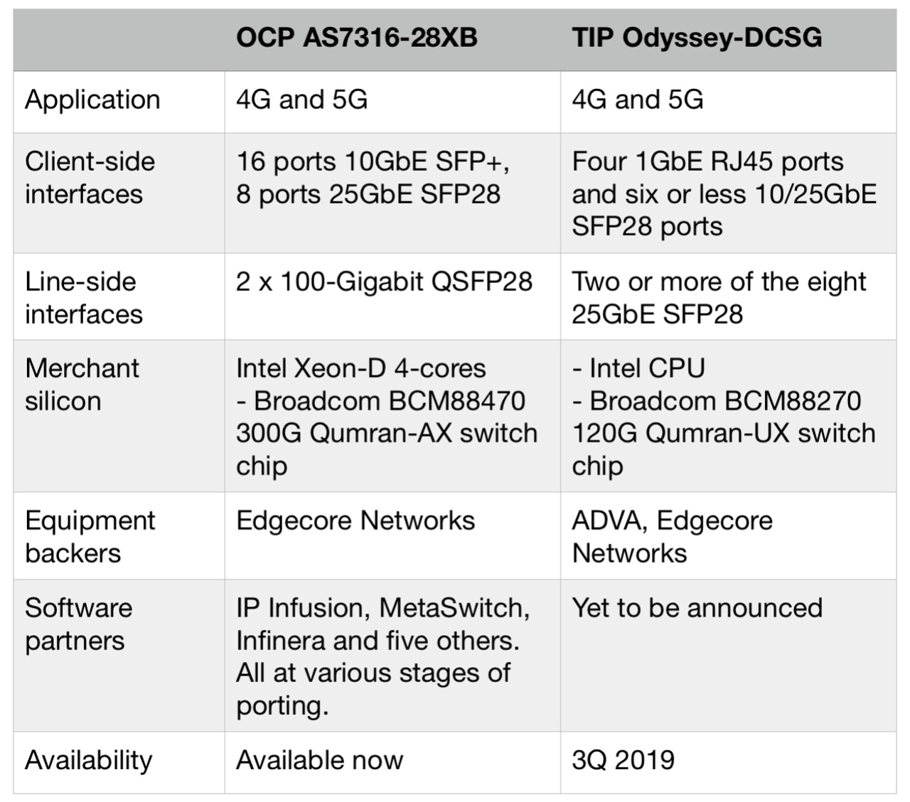
The company is backing two cell-site gateway designs that aggregate traffic from baseband units for 4G and 5G mobile networks. One design is from the Open Compute Project (OCP) that is available now and the second is from the Telecom Infra Project (TIP) that is planned for 2019 (see table).
Edgecore has also announced PON optical line terminal (OLT) platforms addressing 10-gigabit XGS-PON and GPON.
 Source: ADVA, Edgecore Networks
Edgecore is a wholly-ownedsubsidiary of Accton Technology, a Taiwanese original design manufacturer (ODM) employing over 700 networking engineers that reported revenues exceeding $1.2 billion in 2017.
Open networking
Edgecore is a leading proponent of open networking that first data centre operators and now telecom operators are adopting.
Open networking refers to disaggregated designs where the hardware and software comes from separate companies. The hardware is a standardised white box developed in an open framework, while the accompanying software can be commercial code from a company or open-sourced.
Our focus is on all those attributes of open networking: disaggregation, the hardware and software design of standard platforms, and making those designs open
Telecom networks have traditionally been built using proprietary equipment from systems vendors that includes the complete software stack. But the leading telcos have moved away from this approach to avoid being locked into a systems vendor's roadmap. Instead, they are active in open frameworks and are embracing disaggregated open designs, having seen the benefits achieved by the internet content providers that pioneered the approach.
“The IT industry for years have been buying servers and purposing them for whatever application they are designated for, adding an operating system and application software on top,” says Mark Basham, vice president business development and marketing, EMEA at Edgecore. “Now we are seeing the telecom industry shift to that model; they see where the value should be.”
White-box platforms built using merchant silicon promise to reduce the number of specialised platforms in an operator’s network, reducing costs by simplifying platform qualification and support.
“Our focus is on all those attributes of open networking: disaggregation, the hardware and software design of standard platforms, and making those designs open,” says Bill Burger, vice president, business development and marketing for North America at Edgecore.
OCP, TIP and ONF
Edgecore is active in three leading open framework initiatives whose memberships include large-scale data centre operators, telcos, equipment makers, systems integrators, software partners and chip players.
Edgecore is a member of OCP that was founded to address the data centre but now plays an important role in telecoms. The company is also part of TIP that was established in 2016 and includes internet giants Facebook and Microsoft as well as leading telecom operators, systems vendors, components players and others. Edgecore is also a key white-box partner as part of the Open Networking Foundation’s (ONF) reference-design initiative.
 Edgecore Networks' involvement in the ONF's reference design projects. Diagram first published in July 2018. Source: ONF.
Cell-site gateways
Edgecore has announced the availability of its AS7316-26XB, the industry’s first open cell-site gateway white-box design from the OCP that originated as an AT&T specification.
The company is also active in TIP’s cell-site gateway initiative. Edgecore will make and market the Odyssey Disaggregated Cell Site Gateway (Odyssey-DCSG) design that is backed by TIP’s operator members Telefonica, Orange, TIM Brazil and Vodafone. BT is also believed to be backing the TIP gateway.
The gateway aggregates the radio baseband unit (BBU) at a cell site back into the transport network.
The OCP cell-site gateway has a more advanced specification compared to the Odyssey. The AS7316-26XB uses a more powerful Intel processor and employs a 300-gigabit Broadcom Qumran-AX switch chip that aggregates the baseband traffic for transmission into the network.
The platform’s client-side interfaces include 16 SFP+ ports that supports either 1 Gigabit Ethernet (GbE) SFP or 10GbE SFP+ pluggable modules, eight 25GbE ports that accommodate either 10GbE SFP+ or 25GbE SFP28 modules, and two 100GbE QSFP28 uplinks. Some of the 25GbE ports could be used to expand the uplink capacity, if needed.
In contrast, the TIP Odyssey-DCSG platform uses a 120-gigabit Qumran switch chip while its interfaces include provide four 1GbE RJ45 ports and eight 10GbE or 25GbE SFP28 ports. Accordingly, the platform’s uplinks are at 25GbE.
“They [the OCP and TIP gateways] are very different boxes in terms of their performance,” says Basham.
Current deployed mobile platforms don't have sufficient capacity to support LTE Advanced Pro, never mind 5G, says Basham: “All the operators are looking at what is the right time to insert these boxes in the network.”
Telcos need to decide how much they are willing to spend up front. They could deploy a larger capacity but costlier cell-site gateway to future-proof their mobile backhaul for up to a decade. Or they could install the smaller-capacity Odyssey-DCSG that will suffice for five years before requiring an upgrade.
Given that the largest operators will deploy the gateways in units of hundreds of thousands, the capital expenditure outlay will be significant.
Basham says there will be a family of cell-site gateways and points out that the TIP specification originally had three ‘service configurations’. The latest TIP specification document now has a fourth service configuration that differs significantly from the other three in its port count and capabilities. “It shows that there is no one-size-fits-all,” says Basham.
The company also has announced two open disaggregated PON products, part of the OCP.
The ASXvOLT16 is a 10-gigabit OLT platform that supports XGS-PON and NG-PON2. The open OLT platform uses Broadcom’s 800-gigabit Qumran-MX switch chip and its BCM68620 Maple OLT device.
The platform’s interfaces includes 16 XFP ports supporting 10-gigabit optics while for the uplink traffic, four 100GbE ports are used. Each 10-gigabit interface will support 32 or 64 PON optical network units (ONU) typically.
“To support NG-PON2 will require the virtual OLT hardware abstraction layer to be adapted slightly, and also firmware to be put on the Broadcom chips,” says Basham. “The big difference between XGS-PON and NG-PON2 is in the plug-in optics.” More costly tunable optics will be required for NG-PON2. The 1 rack unit (1RU) PON OLT design is available now.
Edgecore has also contributed GPON OLT designs that conform with Deutsche Telecom’s Open GPON OLT design. The Edgecore ASGvOLT32 and ASGvOLT64 GPON OLTs support 32- and 64-GPON ports, respectively, while there are two 100GbE and eight 25GbE uplink ports.
The two GPON OLTs will sample in the first quarter of 2019, moving to volume production one quarter later.
We are at the cusp of bringing together all the parts to make Cassini a deployable solution
Cassini
Edgecore is also bringing its Cassini packet-optical transport white-box platform to market.
Like TIP’s Voyager box, Cassini uses the Broadcom StrataXGS Tomahawk 3.2-terabit switch chip. But while the Voyager comes with built-in coherent interfaces based on Acacia’s AC-400 module, Cassini is a modular design that has eight card slots. Each slot can accommodate one of three module options: a coherent CFP2-ACO, a coherent CFP2-DCO or two QSFP28 100-gigabit pluggables. The Cassini platform also has 16 fixed QSFP28 ports.
Accordingly, the 1.5RU Cassini box can be configured using only the coherent interfaces required. The box could be set up as a 3.2-terabit switch using QSFP28 modules only or as a transport box with up to 1.6 terabits of client-side interfaces and 1.6 terabits of line-side coherent interfaces. This contrasts with the 1RU Voyager that offers 2 terabits of switch capacity with its dozen 100-gigabit client-side interfaces and 800 gigabits of coherent line-side capacity.
“We are at the cusp of bringing together all the parts to make Cassini a deployable solution,” says Basham. “The focus is to get it deployed in the market.”
Edgecore sees Cassini as a baseline for future products. One obvious direction is to increase the platform’s capacity using Broadcom’s 12.8-terabit Tomahawk 3 switch chip. Edgecore already offers a Tomahawk 3-based switch for the data centre.
Such a higher-capacity Cassini platform would support 400GbE client-side interfaces and 400- or 800-gigabit coherent line-side interfaces. “We think that there is a future need for such a platform but we are not actively developing it right now,” says Burger.
A second direction for Cassini’s development is as a platform suited to routeing using larger look-up tables and deep buffering. Such a platform would use merchant silicon such as Broadcom’s Jericho chip. “We think there is a need for that as service providers deploy packet transport platforms in their networks,” says Burger.
Business model
The Cassini platform arose as part of Edgecore’s detailed technology planning discussions with its leading internet content provider customers.
“We recognised a need for more modularity in an open-packet transponder, the ability to mix-and-match the number of packet switching interfaces with the coherent optical interfaces,” says Burger.
Edgecore then approached TIP before contributing the Cassini platform to the organisation’s Open Optical and Packet Transport group.
When Edgecore contributes a design to an open framework such as the OCP or TIP, the design undergoes a review resulting in valuable feedback from member companies.
“We end up making modifications to improve the design in some cases and it then goes through an approval process,” says Burger. “After that, we contribute the design package and its available to anyone without any royalty obligation.”
At first glance, it is not obvious how contributing a platform design that other firms can build benefits Edgecore. But Burger says Edgecore benefits is several ways.
The organisation members’ feedback improves the product’s design. Edgecore also raises industry awareness of its platforms including among the OCP’s and TIP’s large service provider members.
Making the design available to members also offers the operators a potential second source for Edcore’s white box designs, strengthening confidence and their appeal.
And once a design is open sourced, software partners including start-ups will investigate the design as a platform for their code which can result in partnerships. “This benefits us and benefits the software companies,” says Burger.
Edgecore stresses that open-networking platforms are going to take time before they become widely adopted across service providers’ networks.
“It is going to be an evolution, starting with high-volume, more standardised use cases,” concludes Burger.
Part 1: TIP white-box designs, click here
Switch chips not optics set the pace in the data centre
Broadcom is doubling the capacity of its switch silicon every 18-24 months, a considerable achievement given that Moore’s law has slowed down.
Last December, Broadcom announced it was sampling its Tomahawk 3 - the industry’s first 12.8-terabit switch chip - just 14 months after it announced its 6.4-terabit Tomahawk 2.
 Rochan SankarSuch product cycle times are proving beyond the optical module makers; if producing next-generation switch silicon is taking up to two years, optics is taking three, says Broadcom.
“Right now, the problem with optics is that they are the laggards,” says Rochan Sankar, senior director of product marketing at switch IC maker, Broadcom. “The switching side is waiting for the optics to be deployable.”
The consequence, says Broadcom, is that in the three years spanning a particular optical module generation, customers have deployed two generations of switches. For example, the 3.2-terabit Tomahawk based switches and the higher-capacity Tomahawk 2 ones both use QSFP28 and SFP28 modules.
In future, a closer alignment in the development cycles of the chip and the optics will be required, argues Broadcom.
Switch chips
Broadcom has three switch chip families, each addressing a particular market. As well as the Tomahawk, Broadcom has the Trident and Jericho families (see table).

All three chips are implemented using a 16nm CMOS process. Source: Broadcom/ Gazettabyte.
“You have enough variance in the requirements such that one architecture spanning them all is non-ideal,” says Sankar.
The Tomahawk is a streamlined architecture for use in large-scale data centres. The device is designed to maximise the switching capacity both in terms of bandwidth-per-dollar and bandwidth-per-Watt.
“The hyperscalers are looking for a minimalist feature set,” says Sankar. They consider the switching network as an underlay, a Layer 3 IP fabric, and they want the functionality required for a highly reliable interconnect for the compute and storage, and nothing more, he says.
Right now, the problem with optics is that they are the laggards
Production of the Tomahawk 3 integrated circuit (IC) is ramping and the device has already been delivered to several webscale players and switch makers, says Broadcom.
The second, Trident family addresses the enterprise and data centres. The chip includes features deliberately stripped from the Tomahawk 3 such as support for Layer 2 tunnelling and advanced policy to enforce enterprise network security. The Trident also has a programmable packet-processing pipeline deemed unnecessary inlarge-scale data centres.
But such features are at the expense of switching capacity. “The Trident tends to be one generation behind the Tomahawk in terms of capacity,” says Sankar. The latest Trident 3 is a 3.2-terabit device.
The third, Jericho family is for the carrier market. The chip includes a packet processor and traffic manager and comes with the accompanying switch fabric IC dubbed Ramon. The two devices can be scaled to create huge capacity IP router systems exceeding 200 terabits of capacity. “The chipset is used in many different parts of the service provider’s backbone and access networks,” says Sankar. The Jericho 2, announced earlier this year, has 10 terabits of capacity.
Trends
Broadcom highlights several trends driving the growing networking needs within the data centre.
One is how microprocessors used within servers continue to incorporate more CPU cores while flash storage is becoming disaggregated. “Now the storage is sitting some distance from the compute resource that needs very low access times,” says Sankar.
The growing popularity of public cloud is also forcing data centre operators to seek greater servers utilisation to ‘pack more tenants per rack’.
There are also applications such as deep learning that use other computing ICs such as graphics processor units (GPUs) and FPGAs. “These push very high bandwidths through the network and the application creates topologies where any element can talk to any element,” says Sankar. This requires a ‘flat’ networking architecture that uses the fewest networking hops to connect the communicating nodes.
Such developments are reflected in the growth in server links to the first level or top-of-rack (TOR) switches, links that have gone from 10 to 25 to 50 and 100 gigabits. “Now you have the first 200-gigabit network interface cards coming out this year,” says Sankar.
Broadcom has been able to deliver 12.8 terabits-per-second in 16nm, whereas some competitors are waiting for 7nm
Broadcom says the TOR switch is not the part of the data centre network experiencing greatest growth. Rather, it is the layers above - the leaf-and-spine switching layers - where bandwidth requirements are accelerating the most. This is because the radix - the switch’s inputs and outputs - is increasing with the use of equal-cost multi-path (ECMP) routing. ECMP is a forwarding technique to distribute the traffic over multiple paths of equal cost to a destination port. “The width of the ECMP can be 4-way, 8-way and 16-way,” says Sankar. “That determines the connectivity to the next layer up.”
It is such multi-layered leaf-spine architectures that the Tomahawk 3 switch silicon addresses.
Tomahawk 3
The Tomahawk 3 is implemented using a 16nm CMOS process and features 256 50-gigabit PAM-4 serialiser-deserialiser (serdes) interfaces to enable the 12.8-terabit throughput.
“Broadcom has been able to deliver 12.8 terabits-per-second in 16nm, whereas some competitors are waiting for 7nm,” says Bob Wheeler, vice president and principal analyst for networking at the Linley Group.
Sankar says Broadcom undertook significant engineering work to move from the 16nm Tomahawk 2’s 25-gigabit non-return-to-zero serdes to a 16nm-based 50G PAM-4 design. The resulting faster serdes design requires only marginally more die area while reducing the gigabit-per-Watt measure by 40 percent.
The Tomahawk 3 also features a streamlined packet-processing pipeline and improved shared buffering. In the past, a switch chip could implement one packet-processing pipeline, says Wheeler. But at 12.8 terabit-per-second (Tbps), the aggregate packet rate exceeds the capacity of a single pipeline. “Broadcom implements multiple ingress and egress pipelines, each connected with multiple port blocks,” says Wheeler. The port blocks include MACs and serdes. “The hard part is connecting the pipelines to a shared buffer, and Broadcom doesn’t disclose details here.”
 Source: Broadcom.
The chip also has telemetry support that exposes packet information to allow the data centre operators to see how their networks are performing.
Adopting a new generation of switch silicon also has system benefits.
One is reducing the number of hops between endpoints to achieve a lower latency. Broadcom cites how a 128x100 Gigabit Ethernet (GbE) platform based on a single Tomahawk 3 can replace six 64x100GbE switches in a two-tier arangement. This reduces latency by 60 percent, from 1 microsecond to 400 nanoseconds.
There are also system cost and power consumption benefits. Broadcom uses the example of Facebook’s Backpack modular switch platform. The 8 rack unit (RU) chassis uses two tiers of switches - 12 Tomahawk chips in total. Using the Tomahawk 3, the chassis can be replaced with a 1RU platform, reducing the power consumption by 75 percent and system cost by 85 percent.
Many in the industry have discussed the possibility of using the next 25.6-terabit generation of switch chip in early trials of in-package optics
Aligning timelines
Both the switch-chip vendors and the optical module players are challenged to keep up with the growing networking capacity demands of the data centre. The fact that next-generation optics takes about a year longer than the silicon is not new. It happened with the transition from 40-gigabit QSFP+ to 100-gigabit QSFP28 optical modules and now from the 100-gigabit QSFP28 to 200 gigabit QSFP56 and 400-gigabit QSFP-DD production.
“400-gigabit optical products are currently sampling in the industry in both OSFP and QSFP-DD form factors, but neither has achieved volume production,” says Sankar.
Broadcom is using 400-gigabit modules with its Tomahawk 3 in the lab, and customers are doing the same. However, the hyperscalers are not deploying Tomahawk-3 based data center network designs using 400-gigabit optics. Rather, the switches are using existing QSFP28 interfaces, or in some cases 200-gigabits optics. But 400-gigabit optics will follow.
The consequence of the disparity in the silicon and optics development cycles is that while the data centre players want to exploit the full capacity of the switch once it becomes available, they can’t. This means the data centre upgrades conducted - what Sankar calls ‘mid-life kickers’ - are costlier to implement. In addition, given that most cloud data centres are fibre-constrained, doubling the number of fibres to accommodate the silicon upgrade is physically prohibitive, says Broadcom.
“The operator can't upgrade the network any faster than the optics cadence, leading to a much higher overall total cost of ownership,” says Sankar. They must scale out to compensate for the inability to scale up the optics and the silicon simultaneously.
Optical I/O
Scaling the switch chip - its input-output (I/O) - presents its own system challenges. “The switch-port density is becoming limited by the physical fanout a single chip can support, says Sankar: “You can't keep doubling pins.”
It will be increasingly challenging to increase the input-output (I/O) to 512 or 1024 serdes in future switchchips while satisfying the system link budget, and achieving both in a power-efficient manner. Another reason why aligning the scaling of the optics and the serdes speeds with the switching element is desirable, says Broadcom.
Broadcom says electrical interfaces will certainly scale for its next-generation 25.6-terabit switch chip.
Linley Group’s Wheeler expects the 25.6-terabit switch will be achieved using 256 100-gigabit PAM4 serdes. “That serdes rate will enable 800 Gigabit Ethernet optical modules,” he says. “The OIF is standardising serdes via CEI-112G while the IEEE 802.3 has the 100/200/400G Electrical Interfaces Task Force running in parallel.”
But system designers already acknowledge that new ways to combine the switch silicon and optics are needed.
“One level of optimisation is the serdes interconnect between the switch chip and the optical module itself,” says Sankar, referring to bringing of optics on-board to shorten the electrical paths the serdes must drive. The Consortium of On-Board Optics (COBO) has specified just such an interoperable on-board optics solution.
“The stage after that is to integrate the optics with the IC in a single package,” says Sankar.
Broadcom is not saying which generation of switch chip capacity will require in-package optics. But given the IC roadmap of doubling switch capacity at least every two years, there is an urgency here, says Sankar.
The fact that there are few signs of in-package developments should not be mistaken for inactivity, he says: “People are being very quiet about it.”
Brad Booth, chair of COBO and principal network architect for Microsoft’s Azure Infrastructure, says COBO does not have a view as to when in-package optics will be needed.
Discussions are underway within the IEEE, OIF and COBO on what might be needed for in-package optics and when, says Booth: “One thing that many people do agree upon is that COBO is solving some of the technical problems that will benefit in-package optics such as optical connectivity inside the box.”
The move to in-package optics represents a considerable challenge for the industry.
“The transition and movement to in-package optics will require the industry to answer a lot of new questions that faceplate pluggable just doesn’t handle,” says Booth. “COBO will answer some of these, but in-package optics is not just a technical challenge, it will challenge the business-operating model.”
Booth says demonstrations of in-package optics can already be done with existing technologies. And given the rapid timelines of switch chip development, many in the industry have discussed the possibility of using the next 25.6-terabit generation of switch chip in early trials of in-package optics, he says.
There continues to be strong interest in white-box systems and strong signalling to the market to build white-box platforms
White boxes
While the dominant market for the Tomahawk family is the data centre, a recent development has been the use the 3.2-terabit Tomahawk chip within open-source platforms such as the Telecom Infra Project’s (TIP) Voyager and Cassini packet optical platforms.
Ciena has also announced its own 8180 platform that supports 6.4 terabits of switching capacity, yet Ciena says the 8180 uses a Tomahawk 3, implying the platform will scale to 12.8Tbps.
Niall Robinson,vice president, global business development at ADVA, a member of TIP and the Voyager initiative, makes the point that since the bulk of the traffic remains within the data centre, the packet optical switch capacity and the switch silicon it uses need not be the latest generation IC.
“Eventually, the packet-optical boxes will migrate to these larger switching chips but with some considerable time lag compared to their introduction inside the data centre,” says Robinson.
The advent of 400-gigabit client-port optics will drive the move to higher-capacity platforms such as the Voyager because it is these larger chips that can support 400-gigabit ports. “Perhaps a Jericho 2 at 9.6-terabit is sufficient compared to a Tomahawk 3 at 12.8-terabit,” says Robinson.
Edgecore Networks, the originator of the Cassini platform, says it too is interested in the Tomahawk 3 for its Cassini platform.
“We have a Tomahawk 3 platform that is sampling now,” says Bill Burger, vice president, business development and marketing, North America at Edgecore Networks, referring to a 12.8Tbps open networking switch that supports 32, 400-gigabit QSFP-DD modules that has been contributed to the Open Compute Project (OCP).
Broadcom’s Sankar highlights the work of the OCP and TIP in promoting disaggregated hardware and software. The initiatives have created a forum for open specifications, increased the number of hardware players and therefore competition while reducing platform-development timescales.
“There continues to be strong interest in white-box systems and strong signalling to the market to build white-box platforms,” says Sankar.
The issue, however, is the lack of volume deployments to justify the investment made in disaggregated designs.
“The places in the industry where white boxes have taken off continues to be the hyperscalers, and a handful of hyperscalers at that,” says Sankar. “The industry has yet to take up disaggregated networking hardware at the rate at which it is spreading at least the appearance of demand.”
Sankar is looking for the industry to narrow the choice of white-box solutions available and for the emergence of a consumption model for white boxes beyond just several hyperscalers.