
Tomahawk 6: The industry’s first 100-terabit switch chip

Part 2: Data Centre Switching
Peter Del Vecchio, product manager for the Tomahawk switch family at Broadcom, outlines the role of the company’s latest Tomahawk 6 Ethernet switch chip in AI data centres.
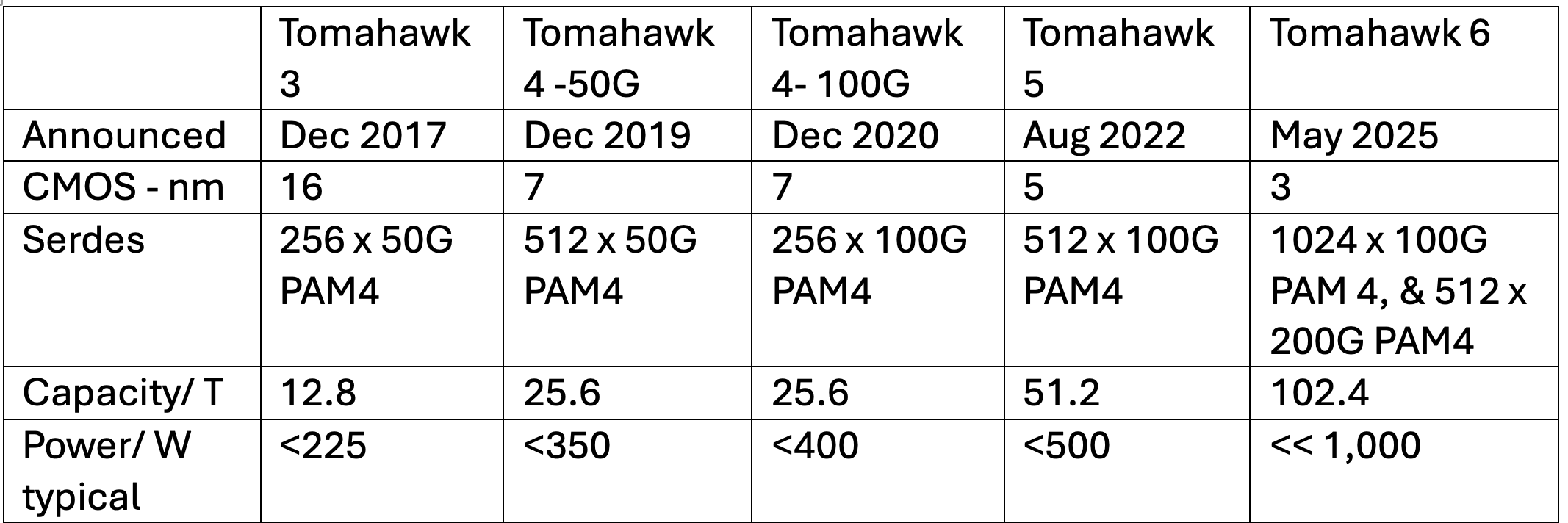
Broadcom is now shipping samples of its Tomahawk 6, the industry’s first 102.4-terabit-per-second (Tbps) Ethernet switch chip. The chip highlights AI’s impact on Ethernet networking switch chip design since Broadcom launched its current leading device, the 51.2-terabit Tomahawk 5. The Tomahawk 6 is more evolutionary, rather than a complete change, notes Del Vecchio. The design doubles bandwidth and includes enhanced networking features to support AI scale-up and scale-out networks.
Nvidia is the only other company that has announced a 102.4 terabit switch, and it’s scheduled for production in 2026,” says Bob Wheeler, analyst at large at market research firm LightCounting, adding that Nvidia sells switches, not chips.
Multi-die architecture
The Tomahawk 6 marks a shift from the monolithic chip design of the Tomahawk 5 to a multi-die architecture.
The 102.4 terabit Tomahawk 6 comes in two versions. One has 512 input-output lanes – serialisers/ deserialisers (serdes) – operating at 200-gigabit using 4-level pulse amplitude modulation signalling (PAM-4). The other Tomahawk 6 version has 1,024 serdes, each using 100-gigabit PAM-4.
“The core die is identical between the two, the only difference are the chiplets that are either for 100 gig or 200 gig PAM-4,” says Del Vecchio. The core die hosts the packet processing and traffic management logic.
The chip uses a 3nm CMOS process node, which improves power efficiency compared to the 5nm CMOS Tomahawk 5.
Broadcom does not quote exact power figures for the chip. “The Tomahawk 6 is significantly less than one watt per 100 gigabits-per-second, well below 1,000 watts,” says Del Vecchio. In contrast, the Tomahawk 5 consumes less than 512 watts.
AI networking: Endpoint-scheduled fabrics
The Tomahawk 6 chip is designed for AI clusters requiring near-100 per cent network utilisation.
“With previous data centre networks, it was unusual that the networks would be loaded to more than 60 to 70 per cent utilisation,” says Del Vecchio. “For AI, that’s unacceptable.”
The chip supports endpoint-scheduled fabrics, where traffic scheduling and load balancing occur at the endpoints to ensure the traffic is efficiently distributed across the network. An endpoint could be a network interface card (NIC) or an AI accelerator interface.
This contrasts with Broadcom’s other switch chip family, the Jericho 3-AI and the Ramon, which is designed for switch-scheduled fabrics. Here, the switch chip handles the networking and packet spraying, working alongside simpler end-point hardware.
The type of switch chip used – endpoint schedule or switch scheduled – depends on the preferences of service providers and hyperscalers. Broadcom says there is demand for both networking approaches.
The Tomahawk 6 uses Broadcom’s latest cognitive routing suite and enhanced telemetry to address the evolving AI traffic patterns.
The market shifted dramatically in 2022, says Del Vecchio, with demand moving from general data centre networking to one focused on AI’s needs. The trigger was the generative AI surge caused by the emergence of ChatGPT in November 2022, after the Tomahawk 5 was already shipping.
“There was some thought of AI training and for inference [with the Tomahawk 5], but the primary use case at that point was thought to be general data centre networks,” says Del Vecchio.
Wide and flat topologies
Tomahawk 6 supports two-tier networks connecting up to 128,000 AI accelerator chips, such as graphic processor units (GPUs). This assumes 200 gigabits per endpoint, which may be insufficient for the I/O requirements of the latest AI accelerator chips.
To achieve higher bandwidth per end-point – 800 gigabit or 1.6 terabit – multiple network planes are used in parallel, each adding 200 gigabits. This way, Broadcom’s design avoids adding an extra third tier of network switching.
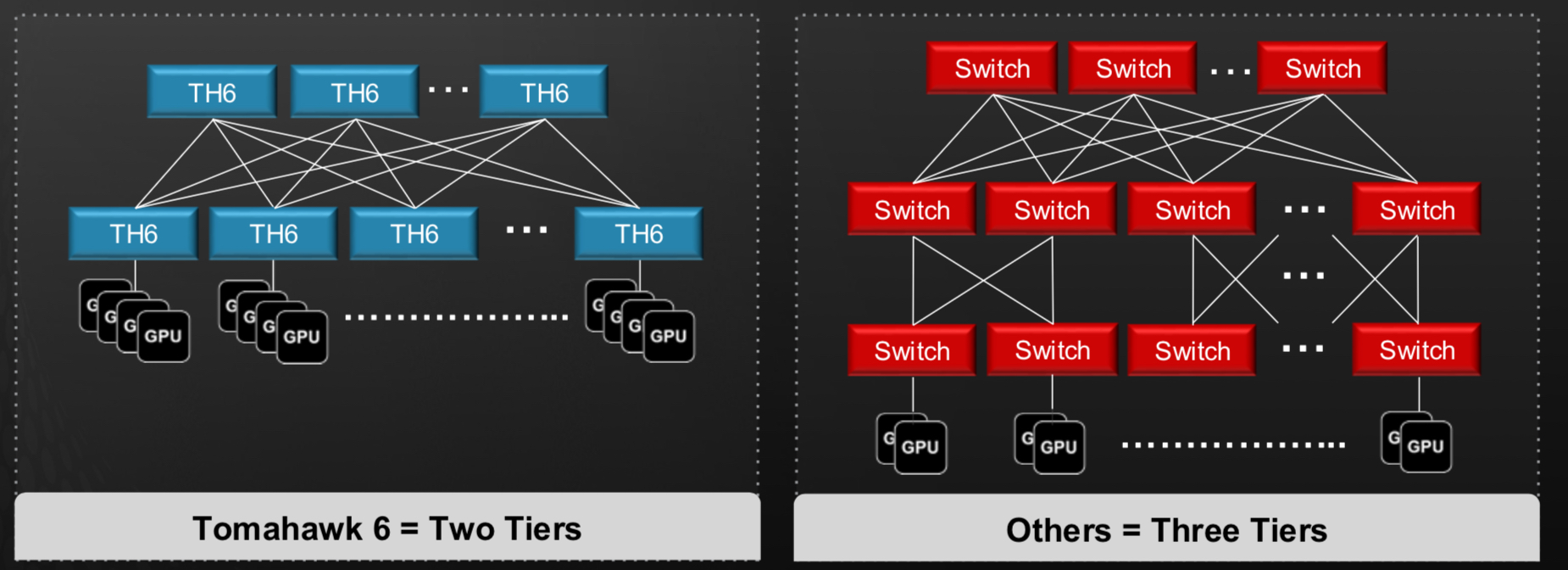
“Rather than having three tiers, you have multiple networking planes, say, eight of those in parallel,” says Del Vecchio.Such a wide-and-flat topology minimises latency and simplifies congestion control, which is critical for AI workloads. “Having a two-tier network versus a three-tier network makes congestion control much easier,” he says.
Tomahawk 6’s enhanced adaptive routing and load balancing features caters to AI’s high-utilisation demands. The aim is to try to keep the port speed low, to maximise the radix, says Del Vecchio, contrasting AI networks with general data centres, where higher 800-gigabit port speeds are typical.
Scale-Up Ethernet
The above discussion refers to the scale-out networking approach. For scale-up networking, the first hop between the AI accelerator chips, the devices are densely interconnected using multiple lanes — four or eight 200-gigabit lanes — to achieve higher bandwidth within a rack.
Broadcom has taken a different approach to scale-up networking than other companies. It has chosen Ethernet rather than developing a proprietary interface like Nvidia’s NVlink or the industry-backed UALink.
Broadcom has released its Scale-Up Ethernet (SUE) framework, which positions Ethernet as a unified solution for scale-up networks and which it has contributed to the Open Compute Project (OCP).

SUE supports large-scale GPU clusters. “You can do 512 XPUs in a scale-up cluster, connected in a single hop,” says Del Vecchio. SUE’s features include link-level retry, credit-based flow control, and optimised headers for low-latency, reliable transport.
“There is no one-size-fits-all for scale-up,” says Wheeler. “For example, Google’s ICI [inter chip interconnect] is a remote direct memory access (RDMA) based interconnect, more like Ethernet than UALink or NVLink,” says Wheeler. “There will likely be multiple camps.”
Broadcom chose Ethernet for several reasons. “One is you can leverage the whole Ethernet ecosystem,” says Del Vecchio, who stresses it results in a unified toolset for front-end, back-end, and scale-up networks.
SUE also aligns with hyperscaler preferences for interchangeable interfaces. “They’d like to have one unified technology for all that,” says Del Vecchio.
Del Vecchio is also a Ultra Ethernet Consortium (UEC) steering committee member. The UEC focuses on scale-out for its 1.0 specification, which is set for public release soon.
Link-level retry (LLR) and credit-based flow control (CBFC) are already being standardised within UEC, says Del Vecchio, and suggests that there will also be scale-up extensions which will benefit Broadcom’s SUE approach.
Interconnects
Tomahawk 6 supports diverse physical interconnects, including 100-gigabit and 200-gigabit PAM-4 serdes and passive copper links up to 2 meters, enabling custom GPU cluster designs.

“There’s a lot of focus on these custom GPU racks,” says Del Vecchio, highlighting the shift from generic pizza-box switches to highly engineered topologies.
The goal is to increase the power to each rack to cram more AI accelerator chips, thereby increasing the degree of scale-up using copper interconnect. Copper links could be used to connect two racks to further double scale-up capacity.
Co-packaged optics: Enhancing reliability?
Co-packaged optics (CPO) has also become a design feature of switch chips. The Tomahawk 6 will be Broadcom’s third-generation switch chip that will also be offered with co-packaged optics.
“People are seeing how much power is going into the optics for these GPU racks,” says Del Vecchio. Co-packaged optics eliminates retimers and DSPs, reducing latency and burst errors
Broadcom and hyperscalers are currently investigating another key potential benefit of co-packaged optics. “There are indications that you wind up with significantly fewer link flaps,” he said. A link flap refers to an link instability.
Unlike pluggable optics, which introduce burst errors via DSPs, co-packaged optics offers random Gaussian noise, which is better suited for forward error correction schemes. “If you have an end-to-end CPO link, you have much more random errors,” he explained.
This suggests that using co-packaged optics could benefit the overall runtime of massive AI clusters, a notable development that, if proven, will favour the technology’s use. “We expect the Tomahawk 6 Davisson co-packaged optics version to follow Tomahawk 6 production closely,” says LightCounting’s Wheeler.
Design challenges
Tomahawk 6’s development required overcoming significant hurdles.
Packaging over 1,000 serdes was one. “There were no packages on the market anywhere near that size,” says Del Vecchio, emphasising innovations in controlling warpage, insertion loss, and signal integrity. Del Vecchio also highlights the complexity of fanning out 1,000 lanes. The multi-die design required low-latency, low-power chip-to-chip interfaces, with Broadcom using its experience developing custom ASICs.
Traffic management structures, like the Memory Management Unit (MMU), have also seen exponential complexity increases. “Some structures are 4x the complexity,” says Del Vecchio.
The multi-die design demanded efficient chip-to-chip interfaces, while packaging 1,000 serdes lanes required signal integrity and manufacturability innovations. “We spent a lot of time on the packaging technology,” he added.
Meanwhile, using architectural optimisations, such as automatic clock gating and efficient serdes design, improved power efficiency. What about the delay in announcing the latest Tomahawk switch chip compared to the clock-like 2-year launch date gaps of previous Tomahawk chips? (See table above.)
Del Vecchio says the delay wasn’t due to a technical issue or getting access to a 3nm CMOS process. Instead, choosing the right market timing drove the release schedule.
Broadcom believes it has a six-month to one-year lead on competing switch chip makers.
Production and market timing
Tomahawk 6 samples are now shipping to hyperscalers and original equipment manufacturers (OEMs). Production is expected within seven months, matching the timeline achieved with the Tomahawk 5. “We feel confident there is no issue with physical IP,” says Del Vecchio, based on the work done with Broadcom’s test chips and verification suites.
The simultaneous availability of 100-gigabit and 200-gigabit SerDes versions of the latest switch chip reflects AI’s bandwidth demands.
“There is such a huge insatiable demand for bandwidth, we could not afford the time delay between the 100-gig and 200-gig versions,” says Del Vecchio.

II-VI’s VCSEL approach for co-packaged optics
Co-packaged optics was a central theme at this year’s OFC show, held in San Diego. But the solutions detailed were primarily using single-mode lasers and fibre.
The firm II-VI is beating a co-packaged optics path using vertical-cavity surface-emitting lasers (VCSELs) and multi-mode fibre while also pursuing single-mode, silicon photonics-based co-packaged optics.
For multi-mode, VCSEL-based co-packaging, II-VI is working with IBM, a collaboration that started as part of a U.S. Advanced Research Projects Agency-Energy (ARPA-E) project to promote energy-saving technologies.
II-VI claims there are significant system benefits using VCSEL-based co-packaged optics. The benefits include lower power, cost and latency when compared with pluggable optics.
The two key design decisions that achieved power savings are the elimination of the retimer chip – also known as a direct-drive or linear interface – and the use of VCSELs.
The approach – what II-VI calls shortwave co-packaged optics – integrates the VCSELs, chip and optics in the same package.
The design is being promoted as first augmenting pluggables and then, as co-packaged optics become established, becoming the predominant solution for system interconnect.
For every 10,000 QSFP-DD pluggable optical modules used by a supercomputer that are replaced with VCSEL-based co-packaged optics, the yearly electricity bill will be reduced by up to half a million dollars, estimate II-VI and IBM.
VCSEL technology
VCSELs are used for active optical cables and short-reach pluggables for up to 70m or 100m links.
VCSEL-based modules consume fewer watts and are cheaper than single-mode pluggables.
Several factors account for the lower cost, says Vipul Bhatt, vice president of marketing, datacom vertical at II-VI.
The VCSEL emits light vertically from its surface, simplifying the laser-fibre alignment, and multi-mode fibre already has a larger-sized core compared to single-mode fibre.
“Having that perpendicular emission from the laser chip makes manufacturing easier,” says Bhatt. “And the device’s small size allows you to get many more per wafer than you can with edge-emitter lasers, benefitting cost.”
The tinier VCSEL also requires a smaller current density to work; the threshold current of a distributed feedback (DFB) laser used with single-mode fibre is 25-30mA, whereas it is 5-6mA for a VCSEL. “That saves power,” says Bhatt.
Fibre plant
Hyperscalers such as Google favour single-mode fibre for their data centres. Single-mode fibre supports longer reach transmissions, while Google sees its use as future-proofing its data centres for higher-speed transmissions.
Chinese firms Alibaba and Tencent use multi-mode fibre but also view single-mode fibre as desirable longer term.
Bhatt says he has been hearing arguments favouring single-mode fibre for years, yet VCSELs continue to advance in speed, from 25 to 50 to 100 gigabits per lane.
“VCSELs continue to lead in cost and power,” says Bhatt. ”And the 100-gigabit-per-lane optical link has a long life ahead of it, not just for networking but machine learning and high-performance computing.“
II-VI says single-mode fibre and silicon photonics modules are suited for the historical IEEE and ITU markets of enterprise and transport where customers have longer-reach applications.
VCSELs are best suited for shorter reaches such as replacing copper interconnects in the data centre.
Copper interconnect reaches are shrinking as interface speeds increase, while a cost-effective optical solution is needed to support short and intermediate spans up to 70 meters.
“As we look to displace copper, we’re looking at 20 meters, 10 meters, or potentially down to three-meter links using active optical cables instead of copper,” says Bhatt. “This is where the power consumption and cost of VCSELs can be an acceptable premium to copper interconnects today, whereas a jump to silicon photonics may be cost-prohibitive.”
Silicon photonics-based optical modules have higher internal optical losses but they deliver reaches of 2km and 10km.
“If all you’re doing is less than 100 meters, think of the incredible efficiency with which these few milliamps of current pumped into a VCSEL and the resulting light launched directly and efficiently into the fibre,” says Bhatt. “That’s an impressive cost and power saving.”
Applications
The bulk of VCSEL sales for the data centre are active optical cables and short-reach optical transceivers.
“Remember, not every data centre is a hyperscale data centre,” says Bhatt. ”So it isn’t true that multi-mode is only for the server to top-of-rack switch links. Hyperscale data centres also have small clusters for artificial intelligence and machine learning.”
The 100m-reach of VCSELs-based optics means it can span all three switching tiers for many data centres.
The currently envisioned 400-gigabit VCSEL modules are 400GBASE-SR8 and the 8-by-50Gbps 400G-SR4.2. Both use 50-gigabit VCSELs: 25 gigabaud devices with 4-level pulse amplitude modulation (PAM-4).
The 400GBASE-SR8 module requires 16 fibres, while the 400G-SR4.2, with its two-wavelength bidirectional design, has eight fibres.
The advent of 100-gigabit VCSELs (50 gigabaud with PAM-4) enables 800G-SR8, 400G-SR4 and 100G-SR1 interfaces. II-VI first demonstrated a 100-gigabit VCSEL at ECOC 2019, while 100-gigabit VCSEL-based modules are becoming commercially available this year.
Terabit VCSEL MSA
The Terabit Bidirectional (BiDi) Multi-Source Agreement (MSA) created earlier this year is tasked with developing optical interfaces using 100-gigabit VCSELs.
The industry consortium will define 800 gigabits interface over parallel multi-mode fibre, the same four pairs of multi-mode fibre that support the 400-gigabit, 400G-BD4.2 interface. It will also define a 1.6 terabit optical interface.
The MSA work will extend the parallel fibre infrastructure from legacy 40 gigabits to 1.6 terabits as data centres embrace 25.6-terabit and soon 51.2-terabit switches.
Founding Terabit BiDi MSA members include II-VI, Alibaba, Arista Networks, Broadcom, Cisco, CommScope, Dell Technologies, HGGenuine, Lumentum, MACOM and Marvell Technology.
200-gigabit lasers and parallelism
The first 200-gigabit electro-absorption modulator lasers (EMLs) were demonstrated at OFC ’22, while the next-generation 200-gigabits directly modulated lasers (DMLs) are still in the lab.
When will 200-gigabit VCSELs arrive?
Bhatt says that while 200-gigabit VCSELs were considered to be research-stage products, recent interest in the industry has spurred the VCSEL makers to accelerate the development timeline.
Bhatt repeats that VCSELs are best suited for optimised short-reach links.
“You have the luxury of making tradeoffs that longer-reach designs don’t have,” he says. “For example, you can go parallel: instead of N-by-200-gig lanes, it may be possible to use twice as many 100-gig lanes.”
VCSEL parallelism for short-reach interconnects is just what II-VI and IBM are doing with shortwave co-packaged optics.
Shortwave co-packaged optics
Computer architectures are undergoing significant change with the emergence of accelerator ICs for CPU offloading.
II-VI cites such developments as Nvidia’s Bluefield data processing units (DPUs) and the OpenCAPI Consortium, which is developing interface technology so that any microprocessor can talk to accelerator and I/O devices.
“We’re looking at how to provide a high-speed, low-latency fabric between compute resources for a cohesive fabric,” says Bhatt. The computational resources include processors and accelerators such as graphic processing units (GPUs) and field-programmable gate arrays (FPGAs).
II-VI claims that by using multi-mode optics, one can produce the lowest power consumption optical link feasible, tailored for very-short electrical link budgets.
The issue with pluggable modules is connecting them to the chip’s high-speed signals across the host printed circuit board (PCB).
“We’re paying a premium to have that electrical signal reach through,” says Bhatt. “And where most of the power consumption and cost are is those expensive chips that compensate these high-speed signals over those trace lengths on the PCB.”
Using shortwave co-packaged optics, the ASIC can be surrounded by VCSEL-based interfaces, reducing the electrical link budget from some 30cm for pluggables to links only 2-3cm long.
“We can eliminate those very expensive 5nm or 7nm ICs, saving money and power,” says Bhatt.
The advantage of shortwave co-packaged optics is better performance (a lower error rate) and lower latency (between 70-100ns) which is significant when connecting to pools of accelerators or memory.
“We can reduce the power from 15W for a QSFP-DD module down to 5W for a link of twice the capacity,” says Bhatt, “We are talking an 80 per cent reduction in power dissipation. Another important point is that when power capacity is finite, every watt saved in interconnects is a watt available to add more servers. And servers bring revenue.”
This is where the 10,000-unit optical interfaces, $0.4-$0.5 million savings in yearly electricity costs comes from.
The power savings arise from the VCSEL’s low drive current, the use of the OIF’s ultra short-reach (USR) electrical interface and the IBM processor driving the VCSEL directly, what is called a linear analogue electrical interface.
In the first co-packaged optics implementation, IBM and II-VI use non-return-to-zero (NRZ) signalling.
The shortwave co-packaged optics has a reach of 20m which enables the potential elimination of top-of-rack switches, further saving costs. (See diagram.)

II-VI sees co-packaged optics as initially augmenting pluggables. With next-generation architectures using 1.6-terabit OSFP-XD pluggables, 20 to 40 per cent of those ports are for sub-20m links.
“We could have 20 to 40 per cent of the switch box populated with shortwave co-packaged optics to provide those links,” says Bhatt.
The remaining ports could be direct-attached copper, longer-reach silicon-photonics modules, or VCSEL modules, providing the flexibility associated with pluggables.
“We think shortwave co-packaged optics augments pluggables by helping to reduce power and cost of next-generation architectures.”
This is the secret sauce of every hyperscaler. They don’t talk about what they’re doing regarding machine learning and their high-performance systems, but that’s where they strive to differentiate their architectures, he says.
Status
Work has now started on a second-generation shortwave design that will use PAM-4 signalling. “That is targeted as a proof-of-concept in the 2024 timeframe,” says Bhatt.
The second generation will enable a direct comparison in terms of power, speed and bandwidth with single-mode co-packaged optics designs.
Meanwhile, II-VI is marketing its first-phase NRZ-based design.
“Since it is an analogue front end, it’s truly rate agnostic,” says Bhatt. “So we’re pitching it as a low-latency, low-power bandwidth density solution for traditional 100-gigabit Ethernet.”
The design also can be used for next-generation PCI Express and CXL disaggregated designs.
II-VI says there is potential to recycle hyperscaler data centre equipment by adding state-of-the-art network fabric to enable pools of legacy processors. “This technology delivers that,” says Bhatt.
But II-VI says the main focus is for accelerator fabrics: proprietary interfaces like NVlink, Fujitsu’s Tofu interconnect or HPE’s Cray’s Slingshot.
“At some point, memory pools or storage pools will also work their way into the hyperscalers’ data centres,” says Bhatt.
First co-packaged optics switches set for next year
Ranovus says two of its lead customers will deploy co-packaged optics next year.
They will deploy 25.6-terabit Ethernet switch chips but these will be proof-of-concept designs rather than volume deployments.
The deployments will be used to assess the software and gain experience with their maintenance including replacing optics if needed.
“I do think 2024 is going to be the volume year,” says Hamid Arabzadeh, CEO of Ranovus, who expects to announce the customers before the year-end.
Disaggregated server untangles compute, memory and storage elements
Applications
Ranovus is focussed on the emerging integrated optical input-output (I/O) market for Ethernet switches and disaggregated server designs.
A disaggregated server untangles the compute, memory and storage elements found on a server card and pools them separately. This enables a CPU or compute node to access far more memory. It also means each of the server elements can be upgraded independently.
Pooling the memory suits artificial intelligence (AI)/ machine learning applications that process huge data sets. Such applications also require considerable computing.
For machine learning applications, graphic processing unit (GPU) chips are tightly coupled in clusters. But it is a challenge to continually grow the number of GPUs in a cluster and support inter-cluster communications using eletrical interfaces.
Data centre operators want processing performance that scales linearly as more GPUs are adding to a cluster and more clusters are used. This requires longer-reach, high-bandwidth, low-latency links. Limiting the power consumption of such links is also key.
Such system design challenges explain the industry’s interest in adding optical I/O to high-end processors like GPUs. The same applies to Ethernet switch-chips that are doubling in capacity every two years. Moving from electrical to optical interfaces promises longer, energy efficient (measured in pJ/bit), low-latency links.
For Ethernet switch designs, the optical I/O end-point bandwidth needed is at least 3.2 terabits per second (Tbps), says Arabzadeh, whereas for AI it is 0.5-1Tbps.
Odin optical engine
Ranovus recently expanded its optical interconnect portfolio by developing an Odin design that doesn’t need an accompanying retimer chip.
The optical engine combines CMOS and silicon photonics circuits in a monolithic chip, resulting in a smaller, cheaper and power-efficient design.
This second-generation Odin means Ranovus can now offer digital and analogue drive options for co-packaged optics and address more cost-conscious applications such as chip interconnect in servers.
Arabzadeh says its first Odin design that uses a retimer chip helped secure its lead customers.
“We have two lead customers where we are doing the co-packaging of their [switch] chips operating at 100-gigabit PAM-4,” he says. “And we also have an AI customer, where their chip talks PCI Express 5.0 (PCIe 5.0) to our Odin.”
Ranovus first unveiled its Odin-8 800-gigabit design at OFC 2020 and demonstrated it sending eight 100 gigabit PAM-4 (4-level pulse-amplitude modulation) signals, each on a separate fibre.
The design includes a digital retimer IC which takes the OIF-standard extra short reach (XSR) signal – for example, from a switch chip – and recreates (retimes) the PAM-4 signal before forwarding it to Ranovus’ chip. Such a configuration is referred to as a digital-drive design.

“This retimer is not a chip we do and it is expensive,” says Arabzadeh. “It also consumes half the power of the [Odin] chiplet design.”
Ranovus also detailed over a year ago its Odin-32 design that supports four wavelengths per fibre for a total bandwidth of 3.2Tbps.
Since then, Ranovus has developed its Odin-8 for use in an 800-gigabit DR8 optical module. The module will sample and be in the hands of customers for testing in the coming quarter.
The Odin-based 800G-DR8 optical module has a power consumption of 13W; 4W less than rival designs, says Arabzadeh, adding that the optical engine is cost-effective at 400 gigabits, even when using half its capacity.
ODIN version 2.0
The latest monolithic chip is an analogue-drive design. It features radio frequency (RF) drivers, trans-impedance amplifiers (TIAs), silicon photonics transmitters and receivers, and control logic to oversee the components.
The chip does away with clock data recovery (CDR) while integrating the TIAs on-chip. This reduces system costs. “We have the first TIA at 100 gigabits in CMOS,” says Arabzadeh.
To work without the retimer, the monolithic chip is placed much closer to the driving ASIC, with both sharing a common substrate. “It works because it is parked right next to the other chip,” says Arabzadeh.
Ranovus uses a software model of a vendor’s ASIC’s serialiser/ deserialiser (serdes) to ensure the serdes will drive its analogue input.
Being an analogue drive, it is bit-rate and protocol agnostic. “This allows us to get customers beyond the Ethernet market,” says Arabzadeh. These include 100-gigabit PAM-4 signals and the PCIe 5.0 protocol, as mentioned.
For machine learning applications, a proprietary protocol can be used between the end points. NVLink, a serial multi-lane communications link developed by Nvidia, is one such protocol.
Arabzadeh says Ranovus has achieved 1 terabit-per-mm in pitch interface densities: “The stuff we have got involved in with folks in machine learning and AI dwarfs the Ethernet market.”
Laser source
Ranovus’ co-packaged designs use an external laser source. But the company has patented technlogy that allows lasers to be attached directly to the monolithic chip.
This is done at the wafer level, before slicing a wafer to its constituent die. As a result, Ranovus now has two Odin-8 optical engines, one that uses an external laser source (Odin-8ELS) and one with integrated lasers (Odin-8IL)
The laser-attach technology suits optical module designs and expands the company’s optical interconnect toolkit.
The industry has yet to decide whether to adopt a digital or analogue drive approach for co-packaged optics, but the latest Odin design means Ranovus can do both.
Packaging
The company has also been addressing the tricky issue of packaging the chip. “The packaging is a very difficult challenge,” says Arabzadeh.
Ranovus has used the Odin-8 to verify its packaging approach. Two sets of eight fibres are required for the optical I/O (a set to send and a set to receive) and four more fibres are used for the external laser source.
The Odin-32 will use the same packaging and fibre count. What will change is the chip that will support four wavelengths per fibre; instead of the single ring resonator modulator per output, four will be used.
Arabzadeh says each ring modulator is 25 micron so using one or four per path has little impact on the chip’s area.
Market development
Ranovus is addressing both the co-packaged optics and module designs with its Odin designs.
At the OFC conference and exhibition this summer, Arista Networks outlined how pluggable optics will be able to address 102.4 terabit Ethernet switches while Microsoft said it expects to deploy co-packaged optics by the second half of 2024.
Because of the uncertainty as to when co-packaged optics will take off, Ranovus will also supply its optics for the 400-gigabit and 800-gigabit pluggable module market.
“That is why we have yet to tape out the Odin-32,” he says. “We didn’t want to have the technology and there is nobody on the other side of it.”
But the key is to have an optical interface portfolio that secures designs early.
“If you can get the wins and through that, modify your chip, then you are designed in,” says Arabzadeh.