Broadcom has detailed its first silicon for the sixth generation of the PCI Express (PCIe 6.0) bus, developed with AI servers in mind.
The two types of PCIe 6.0 devices are a switch chip and a retimer.
Broadcom, working with Teledyne LeCroy, is also making available an interoperability development platform to aid engineers adopting the PCIe 6.0 standard as part of their systems.
Compute servers for AI are placing new demands on the PCIe bus. The standard no longer about connects CPUs to peripherals but also serving the communication needs of AI accelerator chips.
“AI servers have become a lot more complicated, and connectivity is now very important,” says Sreenivas Bagalkote, Broadcom’s product line manager for the data center solutions group.
Bagalkote describes Broadcom’s PCIe 6.0 switches as a ‘fabric’ rather than silicon to switch between PCIe lanes.
PCI Express
PCIe is an long-standing standard adopted widely, not only for computing and servers but across industries such as medical imaging, automotive, and storage.
The first three generations of PCIe evolved around the CPU. There followed a big wait for the PCIe 4.0, but since then, a new PCI generation has appeared every two years, each time doubling the data transfer rate.
Now, PCIe 6.0 silicon is coming to the market while work continues to progress on the latest PCIe 7.0, with the final draft ready for member review.
The PCIe standard supports various lane configurations from two to 32 lanes. For servers, 8-lane and 16-lane configurations are common.
“Of all the transitions in PCIe technology, generation 6.0 is the most important and most complicated,” says Bagalkote.
PCIe 6.0 introduces several new features. Like previous generations, it doubles the lane rate: PCIe 5.0 supports 32 giga-transfers a second (GT/s) while PCIe 6.0 supports 64GT/s.
The 64GT/s line rate requires the use of 4-level pulse amplitude modulation (PAM-4) for the first time; all previous PCIe generations use non-return-to-zero (NRZ) signalling.
Since PCIe must be backwards compatible, the PCIe 6.0 switch supports PAM-4 and NRZ signalling. More sophisticated circuitry is thus required at each end of the link as well as a forward error correction scheme, also a first for the PCIe 6.0 implementation.
Another new feature is flow control unit (FLIT) encoding, a network packet scheme designed to simplify data transfers.
PCIe 6.0 also adds integrity and data encryption (IDE) to secure the data on the PCIe links.
AI servers
A typical AI server includes CPUs, 8 or 16 interconnect GPUs (AI accelerators), network interface cards (NICs) to connect to GPUs making up the cluster, and to storage elements.
A typical server connectivity tray will likely have four switch chips, one for each pair of GPUs, says Bagalkote. Each GPU has a dedicated NIC, typically with a 400 gigabit per second (Gbps) interface. The PCIe switch chips also connect the CPUs and NVMe storage.
Broadcom’s existing generation PCIe 5.0 switch ICs have been used in over 400 AI server designs, estimated by the company at 80 to 90 per cent of all deployed AI servers.
Switch and retimer chips
PCIe 6.0’s doubling the lane data rate makes sending signals over 15-inch rack servers harder.
Broadcom says its switch chip uses serialiser-deserialiser (serdes) that outperform the PCIe specification by 4 decibels (dB). If an extra link distance is needed, Broadcom also offers its PCIe 6.0 retimer chips that also offer an extra 4dB.
Using Broadcom’s ICs at both ends results in a 40dB link budget, whereas the specification only calls for 32dB. “This [extra link budget] allows designers to either achieve a longer reach or use cheaper PCB materials,” says Bagalkote.
The PCIe switch chip also features added telemetry and diagnostic features. Given the cost of GPUs, such features help data centre operators identify and remedy issues they have, to avoid taking the server offline
“PCIe has become an important tool for diagnosing in real-time, remotely, and with less human intervention, all the issues that happen in AI servers,” says Bagalkote.
Early PCIe switches were used in a tree-like arrangement with one input – the root complex – connected via the switch to multiple end-points. Now, with AI servers, many devices connect to each other. Broadcom’s largest device – the PEX90144 – can switches between its 144 PCIe 6.0 lanes while supporting 2-, 4-, 8- or 16-lane-wide ports.
Broadcom also has announced other switch IC configurations with 104- and 88-lanes. These will be followed by 64 and 32 lane versions. All the switch chips are implemented using a 5nm CMOS process.
Broadcom is shipping “significant numbers” of samples of the chips to certain system developers.
PCIe versus proprietary interconnects
Nvidia and AMD that develop CPUs and AI accelerators have developed their own proprietary scale-up architectures. Nvidia has NVLink, while AMD has developed the Infinity Fabric interconnect technology.
Such proprietary interconnect schemes are used in preference to PCIe to connect GPUs, and CPUs and GPUs. However, the two vendors use PCIe in their systems to connect to storage, for example.
Broadcom says that for the market in general, open systems have a history of supplanting closed, proprietary systems. It points to the the success of its PCIe 4.0 and PCIe 5.0 switch chips and believes PCIe 6.0 will be no different.
Disaggregated system vendor developer, Drut Technologies, is now shipping a PCIe 5.0-based scalable AI cluster that can support different vendors’ AI accelerators. Its system uses Broadcom’s 144-lane PCIe 5.0 switch silicon for its interconnect fabric.
Drut is working on its next-generation PCIe 6.0-generation-based design.
Mark Wade, the recently appointed CEO of Ayar Labs, says his new role feels strangely familiar. Wade finds himself revisiting tasks he performed in the early days of the start-up that he helped co-found.
“In the first two years, I would do external-facing stuff during the day and then start working on our chips from 5 PM to midnight,” says Wade, who until last year was the company’s chief technology officer (CTO).
More practically, says Wade, he has spent much of the first months since becoming CEO living out of a suitcase and meeting with customers, investors, and shareholders.
History
Ayar Labs is bringing its technology to market to add high-bandwidth optical input-output (I/O) to large ASICs.
The technology was first revealed in a 2015 paper published in the science journal, Nature. In it, the optical circuitry needed for the interfaces was implemented using a standard CMOS process.
Stojanovic has left his role as a professor at the University of California, Berkeley, to become Ayar Labs’ CTO, following Wade’s appointment as CEO.
Focus
“A few years ago, we made this pitch that machine-learning clusters would be the biggest opportunity in the data centre,” says Wade. “And for efficient clusters, you need optical I/O.” Now, connectivity in artificial intelligence (AI) systems is a vast and growing problem. “The need is there, and our product is timed well,” says Wade.
Ayar Labs has spent the last year focusing on manufacturing and established low-volume production lines. The company manufactured approximately 10,000 optical chiplets in 2023 and expects similar volumes this year. The company also offers an external laser source SuperNova product that provides the light source needed for its optical chiplet.
Ayar Labs’ optical input-output (I/O) roadmap showing the change in electrical I/O interface evolving from Intel’s AIB to the UCIe standard, the move to faster data rates and, on the optical side, more wavelengths and the growing total I/O, per chiplet and packaged system. Source: Ayar Labs.
The products are being delivered to early adopter customers while Ayar Labs establishes the supply chain, product qualification, and packaging needed for volume manufacturing.
Wade says that some of its optical chiplets are being used for other non-AI segments. Ayar Labs has demonstrated its optical I/O being used with FPGAs for electronics systems for military applications. But the primary demand is for AI systems connectivity, whether compute to compute, compute to memory, compute to storage, and compute to a memory-semantic switch.
“A memory-semantic switch allows the scaling of a compute fabric whereby a bunch of devices need to talk to each other’s memory,” says Wade.
Wade cites Nvidia’s NVSwitch as one example: the first layer switch chip at the rack level that supports many GPUs in a non-blocking compute fabric. Another example of a memory-semantic switch is the open standard Compute Express Link (CXL).
The need for co-packaged optics
At the Optica Executive Forum event held alongside the recent OFC show, several speakers questioned the need for I/O based on optical chiplets, also called co-packaged optics.
Google’s Hong Liu, a Distinguished Engineer at Google Technical Infrastructure, described co-packaged optics as an ’N+2 years’ technology, perpetually coming in two years’ time, (N being the current year).
Ashkan Seyedi of Nvidia stressed that copper continues to be the dominant interconnect for AI because it beats optics in such metrics as bandwidth density, power, and cost. Existing data centre optical networking technology cannot simply be repackaged as optical compute I/O, as it does not beat copper. Seyedi also shared a table that showed how much more expensive optical was in terms of dollar per gigabit/second ($/ Gbps).
Wade starts to address these points by pointing out that nobody is making money at the application layer of AI. Partly, this is because the underlying hardware infrastructure for AI is so costly.
“It [the infrastructure] doesn’t have the [networking] throughput or power efficiency to create the headroom for an application to be profitable,” says Wade.
The accelerator chips from the likes of Nvidia and Google are highly efficient in executing the mathematics needed for AI. But it is still early days when it comes to the architectures of AI systems, and more efficient hardware architectures will inevitably follow.
AI workloads also continue to grow at a remarkable rate. They are already so large that they must be spread across systems using ever more accelerator chips. With the parallel processing used to execute the workloads, data has to be shared periodically between all the accelerators using an ’all-to-all’ command.
“With large models, machines are 50 per cent efficient, and they can get down to 30 per cent or even 20 per cent,” says Wade. This means expensive hardware is idle for more than half the time. And the issue will only worsen with growing model size. According to Wade, using optical I/O promises the proper bandwidth density – more terabits-per-second per mm, power efficiency, and latency.
“These products need to get proven and qualified for volume productions,” he adds. “They are not going to get into massive scale systems until they are qualified for huge scale production.”
Wade describes what is happening now as a land grab. Demand for AI accelerators is stripping supply, and the question is still being figured out as to how the economics of the systems can be improved.
“It is not about making the hardware cheaper, just how to ensure the system is more efficiently utilised,” says Wade. “This is a big capital asset; the aim is to have enough AI workload throughput so end-applications have a viable cost.”
This will be the focus as the market hits its stride in the coming two to three years. “It is unacceptable that a $100 million system is spending up to 80 per cent of its time doing nothing,” says Wade.
Wade also addresses the comments made the day at the Optica Executive Forum. “The place where [architectural] decisions are getting discussed and made are with the system-on-chip architects,” he says. “It’s they that decide, not [those at] a fibre-optics conference.”
He also questions the assumption that Google and Nvidia will shun using co-packaged optics.
Market opportunity
Wade does a simple back-of-an-envelope calculation to size the likely overall market opportunity by the early 2030s for co-packaged optics.
In the coming years, there will be 1,000 optical chiplets per server, 1,000 servers per data centre, while 1,000 new data centres using AI clusters will be built. That’s a billion devices in total. Even if the total addressable opportunity is several hundred million optical chiplets, that is still a massive opportunity by 2032, he says.
Wade expects Ayar Labs to ship 100,000 plus chiplets in the 2025-26 timeframe, with volumes ramping to the millions in the two years after that.
“That is the ramp we are aiming for,” he says. “Using optical I/O to build a balanced composable system architecture.” If co-packaged optics does emerge in such volumes, it will disrupt the optical component business and the mainstream technologies used today.
“Let me finish with this,” says Wade. “If we are still having this conversation in two years’ time, then we have failed.”
Broadcom’s Jericho silicon has taken an exciting turn.
The Jericho devices are used for edge and core routers.
But the first chip of Broadcom’s next-generation Jericho is aimed at artificial intelligence (AI); another indicator, if one is needed, of AI’s predominance.
Dubbed the Jericho3-AI, the device networks AI accelerator chips that run massive machine-learning workloads.
AI supercomputers
AI workloads continue to grow at a remarkable rate.
The most common accelerator chip used to tackle such demanding computations is the graphics processor unit (GPU).
GPUs are expensive, so scaling them efficiently is critical, especially when AI workloads can take days to complete.
“For AI, the network is the bottleneck,” says Oozie Parizer, (pictured) senior director of product management, core switching group at Broadcom.
Squeezing more out of the network equates to shorter workload completion times.
“This is everything for the hyperscalers,” says Parizer. “How quickly can they finish the job.”
Broadcom shares a chart from Meta (below) showing how much of the run time for its four AI recommender workloads is spent on networking, moving the data between the GPUs.
Time spent on network for four recommender workloads. Source: Meta
In the worse case, networking accounts for three fifths (57 per cent) of the time during which the GPUs are idle, waiting for data.
Scaling
Parizer highlights two trends driving networking for AI supercomputers.
One is the GPU’s growing input-output (I/O), causing a doubling of the interface speed of network interface cards (NICs). The NIC links the GPU to the top-of-rack switch.
The NIC interface speeds have progressed from 100 to 200 to now 400 gigabits and soon 800 gigabits, with 1.6 terabits to follow.
The second trend is the amount of GPUs used for an AI cluster.
The largest cluster sizes have used 64 or 256 GPUs, limiting the networking needs. But now machine-learning tasks require clusters of 1,000 and 2,000 GPUs up to 16,000 and even 32,000.
Meta’s Research SuperCluster (RSC), one of the largest AI supercomputers, uses 16,000 Nvidia A100 GPUs: 2,000 Nvidia DGX A100 systems each with eight A100 GPUs. The RSC also uses 200-gigabit NICs.
“The number of GPUs participating in an all-to-all exchange [of data] is growing super fast,” says Parizer.
The Jericho3-AI is used in the top-of-rack switch that connects a rack’s GPUs to other racks in the cluster.
The Jericho3-AI enables clusters of up to 32,000 GPUs, each served with an 800-gigabit link.
An AI supercomputer can used all its GPUs to tackle one large training job or split the GPUs into pools running AI workloads concurrently.
Either way, the cluster’s network must be ‘flat’, with all the GPU-to-GPU communications having the same latency.
Because the GPUs exchange machine-learning training data in an all-to-all manner, only when the last GPU receives its data can the computation move onto the next stage.
“The primary benefit of Jericho3-AI versus traditional Ethernet is predictable tail latency,” says Bob Wheeler, principal analyst at Wheeler’s Network. “This metric is very important for AI training, as it determines job-completion time.”
Data spraying
“We realised in the last year that the premium traffic capabilities of the Jericho solution are a perfect fit for AI,” says Parizer.
The Jericho3-AI helps maximise GPU processing performance by using the full network capacity while traffic routing mechanisms help nip congestion in the bud.
The Jericho also adapts the network after a faulty link occurs. Such adaptation must avoid heavy packet loss otherwise the workload must be restarted, potentially losing days of work.
AI workloads use large packet streams known as ‘elephant’ flows. Such flows tie up their assigned networking path, causing congestion when another flow also needs that path.
“If traffic follows the concept of assigned paths, there is no way you get close to 100 per cent network efficiency,” says Parizer.
The Jericho3-AI, used in a top-of-rack switch, has a different approach.
Of the device’s 28.8 terabits of capacity, half connects the rack’s GPUs’ NICs and a half to the ‘fabric’ that links the rack’s GPUs to all the other cluster’s GPUs.
Broadcom uses the 14.4-terabit fabric link as one huge logical pipe over which traffic is evenly spread. Each destination Jericho3-AI top-of-rack switch then reassembles the ‘sprayed’ traffic.
“From the GPU’s perspective, it is unaware that we are spraying the data,” says Parizer.
Receiver-based flow control
Spraying may ensure full use of the network’s capacity, but congestion can still occur. The sprayed traffic may be spread across the fabric to all the spine switches, but for short periods, several GPUs may send data to the same GPU, known as incast (see diagram).
The networking challenges tackled by Jericho3-AI. Source: Broadcom
The Jericho copes with this many-to-one GPU traffic using receiver-based flow control.
Traffic does not leave the receiving Jericho chip just because it has arrived, says Parizer. Instead, the receiving Jericho tells the GPUs with traffic to send and schedules part of the traffic from each.
“Traffic ends up queueing nearer the sender GPUs, notifying each of them to send a little bit now, and now,” says Parizer, who stresses this many-to-one condition is temporary.
Ethernet flow control is used when Jericho chip senses that too much traffic is being sent.
“There is a temporary stop in data transmission to avoid packet loss in network congestion,” says Parizer. “And it is only that GPU that needs to slow down; it doesn’t impact any adjacent GPUs.”
Fault control
At Optica’s Executive Forum event, held alongside the OFC show in March, Google discussed using a 6,000 tensor processor unit (TPU) accelerator system to run large language models.
One Google concern is scaling such clusters while ensuring overall reliability and availability, given the frailty of large-scale accelerator clusters.
“With a huge network having thousands of GPUs, there is a lot of fibre,” says Parizer. “And because it is not negligible, faults happen.”
New paths must be calculated when an optical link goes down in a network arrangement that using flows and assigned paths with significant traffic loss likely.
“With a job that has been running for days, significant packet loss means you must do a job restart,” says Parizer.
Broadcom’s solution, not based on flows and assigned paths, uses load balancing to send data over one less path overall.
Using the Jericho2C+, Broadcom has shown fault detection and recovery in microseconds such that the packet loss is low and no job restart is needed.
The Jericho portfolio of devices
Broadcom’s existing Jericho2 architecture combines an enhanced packet-processing pipeline with a central modular database and a vast memory holding look-up tables.
Look-up tables are used to determine how the packet is treated: where to send it, wrapping it in another packet (tunnel encapsulation), extracting it (tunnel termination), and access control lists (ACLs).
Different stages in the pipeline can access the central modular database, and the store can be split flexibly without changing the packet-processing code.
Jericho2 was the first family device with a 4.8 terabit capacity and 8 gigabytes of high bandwidth memory (HBM) for deep buffering.
The Jericho 2C followed, targeting the edge and service router market. Here, streams have lower bandwidth – 1 and 10 gigabits typically – but need better support in the form of queues, counters and metering, used for controlling packets and flows.
Pariser says the disaggregated OpenBNG initiative supported by Deutsche Telekom uses the Jericho 2C.
Broadcom followed with a third Jericho2 family device, the Jericho 2C+, which combines the attributes of Jericho2 and Jericho2C.
Jericho2C+ has 14.4 terabits of capacity and 144 100-gigabit interfaces, of which 7.2-terabit is network interfacing bandwidth and 7.2-terabit for the fabric interface.
“The Jericho2C+ is a device that can target everything,” says Pariser.
Applications include data centre interconnect, edge and core network routing, and even tiered switching in the data centre.
Hardware design
The Jericho3-AI, made up of tens of billions of transistors in a 5nm CMOS process, is now sampling.
Broadcom says it designed the chip to be cost-competitive for AI.
For example, the packet processing pipeline is simpler than the one used for core and edge routing Jericho.
“This also translates to lower latency which is something hyperscalers also care about,” says Parizer.
The cost and power savings from optimisations will be relatively minor, says Wheeler.
The Jericho3-AI's main attributes. Source: Broadcom
Broadcom also highlights the electrical performance of the Jericho3-AI’s input-output serialiser-deserialiser (serdes) interfaces.
The serdes allows the Jericho3-AI to be used with 4m-reach copper cables linking the GPUs to the top-of-rack switch.
The serdes performance also enables linear-drive pluggables that dont have no digital signal processor (DSP) for retiming with the serdes driving the pluggable directly. Linear drive saves cost and power.
Broadcom’s Ram Valega, senior vice president and general manager of the core switching group, speaking at the Open Compute Project’s regional event held in Prague in April, said 32,000 GPU AI clusters cost around $1 billion, with 10 per cent being the network cost.
NCCL refers to the NVIDIA Collective Communications Library, a set of inter-GPU communication primitives that can be integrated into applications. Performance tests run over NCCL can be used to measure the performance of a workload. Source: Broadcom
Valega showed Ethernet outperforms Infiniband by 10 per cent for a set of networking benchmarks (see diagram above).
“If I can make a $1 billion system ten per cent more efficient, the network pays for itself,” says Valega.
Wheeler says the comparison predates the recently announced NVLink Network, which will first appear in Nvidia’s DGX GH200 platform.
“It [NVLink Network] should deliver superior performance for training models that won’t fit on a single GPU, like large language models,” says Wheeler.
ECOC 2022 included talks on optical switching and co-packaged optics.
Speakers discussed optical switching trends and Google’s revelation that it has been using optical circuit switching in its data centres.
Nvidia discussed its latest chips, how they are used to build high-performance computing systems, and why optical input-output will play a critical role.
Co-packaged optics and optical switching within the data centre were prominent topics at the recent ECOC 2022 conference and exhibition in Basel, Switzerland.
There were also two notable data centre announcements before ECOC.
Tencent announced it would adopt Broadcom’s Humboldt design, a hybrid co-packaged optics version of the Tomahawk 4 switch chip, in its data centres. Tencent is the first hyperscaler to announce it is adopting co-packaged optics.
Google also revealed its adoption of optical circuit switching in its data centres. Google made the revelation in a paper presented at the Sigcomm 2022 conference held in Amsterdam in August.
Optical circuit switching
Google rarely details its data centre architecture, but when it does, it is usually at Sigcomm.
Google first discussed a decade of evolution of its ‘Jupiter’ data centre architecture in a paper at Sigcomm in 2015.
This year, Google gave an update revealing that it has been using optical circuit switching in its data centres for the past five years. As a result, Google can scale its data centre more efficiently using a reconfigurable optical layer.
Upgrading a data centre’s network is much more complex than upgrading servers and storage. Moreover, a data centre is operational far longer than each generation of equipment. It is thus hard for a data centre operator to foresee how equipment and workloads will evolve over the data centre’s lifetime, says Google.
Google would pre-deploy the spine layer when it started operating a data centre. For Google’s Jupiter architecture, 64 spine blocks, each using 40 gigabit-per-second (Gbps) links, would be deployed. Then, Google added newer aggregation blocks with 100Gbps links. But the hyperscaler could not fully benefit due to the pre-existing 40Gbps spine links.
Google wanted to avoid touching the spine switches. A partial upgrade would have limited benefits, while fully upgrading the spine would take months and be hugely disruptive and costly.
Google’s first solution introduced a MEMS-based optical circuit switching layer between the aggregation and spine blocks.
The MEMS-based switch is data rate agnostic and can support multiple generations of optical modules. The switch’s introduction also allowed Google to add new spine blocks alongside new aggregation blocks; the hyperscaler no longer had to pre-deploy the spine.
At some point, Google decided that for new data centre builds, it would use optical circuit switching only and remove the spine layer of electrical switches.
Adopting optical circuit switch-based interconnect changes Google’s data centres from a clos to a direct-connect architecture. However, not all paths are direct; some take two hops to link aggregation blocks.
Google has developed sophisticated control software to best exploit the direct connectivity for traffic flows.
The software also adapts the network topology – the optical links between the aggregation blocks and their capacities. Such topology changes occur every few weeks, with the system first learning the nature of the traffic and workloads.
Removing the spine layer and replacing it with optical circuit switches has reduced Google’s data centre networking costs by 30 per cent and power consumption by 41 per cent.
ECOC reflections about Google’s optical switch adoption
There was much discussion at ECOC of Google’s use of optical circuit switching in its data centres.
S.J. Ben Yoo, a distinguished professor at the University of California, Davis, gave an ECOC talk about new trends in optical switching. “These are expected future trends,” he said. “I don’t have a crystal ball.”
Prof. Ben Yoo stressed the difficulty of scaling up and scaling out data centre networking architectures in the era of artificial intelligence workloads.
He described co-packaged optics as ‘Trend 0’ because it only delivers bandwidth (input-output capacity).
In contrast, introducing a reconfigurable optical switching layer on top of electrical aggregation switches is the first trend in optical switching. This is what Google has done with its optical circuit switch.
The next development in the data centre, says Ben Yoo, will be the introduction of photonic integrated circuit-based optical switching.
Huawei’s Maxim Kuschnerov, in his ECOC talk, said optical switching in the data centre would only grow in importance.
“Are there use cases where we can use optical switching and what are they?” he said. “I like to take a use-case perspective and find a technology that fulfils that use case.”
His view is that with the classical clos architecture, you can’t just rip out a single layer of electrical switches and replace it with optical ones. “There is a reason why you need all these switches and aggregation functionality,” says Kuschnerov.
Kuschnerov views Google’s optical circuit switching as nothing more than an automated patch panel.
“This is not the optical switch which is the saviour of future data centres,” he says.
Mark Filer, optical network architect, systems and services infrastructure at Google, in an ECOC tutorial detailing how Google uses and benefits from standards, multi-source agreements and open-source developments, was asked about Google’s custom optical switch.
Mark Filer, optical network architect, systems and services infrastructure at Google
How could Google explain such a custom design if the hyperscaler is such a proponent of open standards? And would Google consider contributing its optical circuit switch and software design to an open community framework?
“My guess is over time, we may see that it finds its way into some kind of open framework,” said Filer, adding that right now, Google sees its optical circuit switch as delivering a competitive advantage.
Co-packaged optics
Benjamin Lee, a senior research scientist at Nvidia, in his ECOC address, discussed the high-performance computing market and the role graphics processing units (GPUs) play in accelerating artificial intelligence and machine learning tasks.
Nvidia not only develops processors, GPUs and data processing unit ICs but also networking silicon and systems that the company uses to make high-performance computing systems.
Lee’s talk addressed the role optical interconnect will play in ensuring continuing scaling of high-performance GPU-based computing systems.
Scaled systems
Nvidia’s latest GPU, announced earlier this year, is the 80-billion-transistor Hopper H100. The H100 deliver a six-fold improvement in throughput compared to Nvidia’s existing A100 GPU announced in 2020.
The Hopper is Nvidia’s first GPU that uses the latest generation of stacked DRAM memory, known as high bandwidth memory 3 (HBM3). In addition, Hopper also uses Nvidia’s fourth-generation NVlink interface.
Eight H100 GPUs fit within Nvidia’s DGX box, as do four Nvidia NVSwitches used to interconnect the GPUs. In addition, an Nvidia Superpod connects 32 DGX nodes – 256 GPUs – using an external tier of NVSwitches.
“A paradigm shift we’re seeing is that switched interconnect is becoming important for scale-up,” said Lee. “So when we want to make the node more computationally powerful, those switches are being put inside the box to connect the GPUs.”
Switch ASIC bandwidths are consistently improving, with 51.2-terabit switch silicon being state-of-the-art. But despite such progress, the scaling is insufficient to keep up with bandwidth requirements, said Lee.
Switch ASIC power consumption is also rising, with advanced CMOS scaling having less impact on designs. Lee foresees switch ASICs consuming 2kW if current trends continue.
In turn, ASIC input-output (I/O) accounts for an increasing portion of the chip’s overall power consumption.
This is true for Nvidia’s GPUs and switch chips, so any I/O technology developed for switching will also benefit its GPUs.
Thus, Nvidia sees optical I/O as the key to scaling the processing performance of its ASICs and computing systems.
Benjamin Lee, a senior research scientist at Nvidia
I/O metrics
Lee outlined various metrics when discussing optical I/O:
the electrical interfaces used between the ASIC and optics, and their reach
the power consumption of the module (the chip, and the chip and optics)
the system power (of the line card or platform)
interface density: the capacity exiting a millimetre of surface in terabits-per-second-per-mm (Tbps/mm)
For a system using a 102.4-terabit switch IC, half the power is consumed by the ASIC and half by the edge-board pluggable optics. Here the OIF’s long reach (LR) interface links the two.
The chip’s electrical interfaces consume 4.5 to 6.5 picojoule-per-bit (pJ/b) such that the total switch IC I/O power consumed is 450W.
The next step is co-packaged optics. Here, optical chiplets are placed closer to the ASIC (100mm away) such that the OIF’s lower power XSR (extra short reach) interface can be used that consumes 1.24-1.7pJ/s, says Lee.
Again taking a module view, Nvidia views the co-packaged design as comprising two electrical interfaces (the XSR interface between the chip and optical chiplets either side) and one optical interface.
This equates to 250W per chip module, a modest power saving at the chip module level but a significant power saving at the system level, given the optics is now part of the module.
However, bandwidth density is 475-870Gbps/mm, and for beyond 100-terabit switches, a further fourfold improvement is needed: 2Tbps/mm and, ultimately, 10Tbps/mm.
Just achieving a 2Tb/s/mm interface density will be challenging, says Lee.
For that, 2.5D co-packaged optics will be needed with the ASIC and chiplets sharing a silicon interposer that enables higher wire densities.
2.5D integration is already an established technology in the semiconductor industry; Nvidia has been using the technology for its GPUs since 2016.
The technology enables much closer coupling between the ASIC and optics (some 1mm), resulting in sub 1pJ/bit. Nvidia cites research showing a 0.3pJ/b has already been achieved.
Scaling I/O
Lee outlined all the ways I/O can be scaled.
Baud rate is one approach, but the energy efficiency diminishes as the symbol rate increases, from 50 to 100 to 200 gigabaud.
Modulation is another approach, moving from non-return-to-zero to 4-level pulse amplitude modulation (PAM-4) and even higher PAM schemes. The challenge is that the signal-to-noise ratio diminishes the higher the PAM scheme, requiring additional digital signal processing which, in turn, consumes more power.
Another technique, polarization, can be used to double the data rate. Then there is the spatial domain. Here, tighter pitches can be used, says Lee, moving from 250, 127 and even 80 microns before other approaches are needed. These include multi-core fibre, waveguide fan-outs and even bidirectional optics (what Google uses for its optical circuit switch ports, to save on fibre and port count).
All these spatial approaches require considerable development and operational costs, says Lee.
The most promising way to boost throughput and increase interface density is using wavelength division multiplexing (WDM).
Nvidia has produced several generations of test chips that use wavelength parallelism in the O-band based on micro-ring resonators.
Nvidia’s steer
Micro-ring resonator technology already supports 100Gbps modulation rates. The optical circuit is also compact, energy-efficient and supports wavelength scaling.
Lee also outlined other key technologies that will be needed, each bringing their own challenges. One is the external laser source, another is advanced packaging.
Nvidia believes that for future generations of ASICs, dense WDM mirror-ring modulated links offer the most promising approach to meeting both low power and the massive interface density improvements that will be needed.
This will require low-cost lasers while packaging remains a severe challenge.
2.5D integration is going to be an important step in the evolution of switch interconnect, concluded Lee.
Optical interconnect specialist Ayar Labs has announced that it is working with Nvidia, a leader in artificial intelligence (AI) and machine learning silicon, systems and software.
In February Ayar Labs announced a strategic collaboration with the world’s leading high-performance computing (HPC) firm, Hewlett Packard Enterprise (HPE).
Both Nvidia and HPE were part of the Series C funding worth $130 million that Ayar Labs secured in April.
Work partnerships
Ayar Labs has chiplet and external laser source technologies that enable optical input-output (I/O) suited for AI and high-performance computing markets.
Charles Wuischpard, CEO of Ayar Labs, says the work with HPE and Nvidia share common characteristics.
HPE is interested in optical interfaces for high-performance computing fabrics and, in particular, future generations of its Slingshot technology.
Nvidia is also interested in fabrics with its Mellanox technology, but its chips also impact the server. Wuishchpard describes its work with Nvidia as optically enabling Nvidia’s NVLink, its graphics processing unit (GPU) interface.
Nvidia’s optical needs
Bill Dally, chief scientist and senior vice president of research at Nvidia, outlined the company’s interest in optical interconnect at the OFC conference, held in San Diego in March.
Dally started by quantifying the hierarchy of bandwidths and power requirements when sending a bit in computing systems.
The maximum bandwidth and lowest power needs occur, not surprisingly, when data is sent on-chip, between the chip’s processing elements.
With each hierarchical connection jump after that – between chips on an interposer hosting, for example, GPUs and memory (referred to as a module), between modules hosted on a printed circuit board (PCB), linking the boards in a cabinet, and connecting cabinets in a cluster – the bandwidth drops (dubbed bandwidth tapering) and more power is needed to transmit a bit.
There are also different technologies used for the jumps: electrical traces connect the modules on the PCB; electrical cables link the boards in a cabinet (1m to 3m), while active optical cables link the cabinets (5m to 100m).
One issue is that electrical signalling is no longer getting faster (the FO4 delay metric is now constant) with each new CMOS process node. Another issue is that the electrical reach is shrinking with each signalling speed hike: 50-gigabit signals can span 3m, while 200-gigabit signals can span 1m.
Co-packaged optics, where optics are placed next to the IC, promises the best of both worlds: bettering the metrics of PCBs and electrical cable while matching the reach of active optical cables.
Co-packaged optics promises a 5x saving in power when sending a bit compared to a PCB trace while costing a tenth of an active optical cable yet matching its 100m reach. Co-packaged optics also promises a fourfold increase in density (bit/s/mm) compared to PCB traces, says Nvidia.
However, meeting these targets requires overcoming several challenges.
One is generating efficient lasers that deliver aligned frequency grids. Another is getting the micro-ring resonators, used for modulating the data over WDM links, to work reliably and in volume. Nvidia plans to use 8 or 16 micro-ring resonators per WDM link and has developed five generations of test chips that it is still evaluating.
Another issue is packaging the optics, reducing the optical loss when coupling the fibre to the GPU while avoiding the need for active alignment. Cost is a big unknown, says Dally, and if co-packaged optics proves significantly more costly than an electrical cable, it will be a non-starter.
Nvidia outlined an example optical link using 8- or 16-channel WDM links, each channel at 25 gigabit-per-second (Gbps), to enable 200 and 400-gigabit optical links.
Using two polarisations, 800-gigabit links are possible while upgrading each lambda to 50Gbps, and link speed doubles again to 1.6 terabits.
Implementing such links while meeting the cost, power, density and reach requirements is why Nvidia has invested in and is working with Ayar Labs.
“Nvidia has been keeping an eye on us for some time, and they are generally big believers in a micro-ring WDM-based architecture with a remote light source,” says Wuishchpard.
Nvidia is optimistic about overcoming the challenges and that in the coming years – it won’t say how many – it expects electrical signalling to be used only for power. At the same time, co-packaged optics will handle the interconnect.
Nvidia detailed a conceptual GPU architecture using co-packaged optics.
Each GPU would be co-packaged with two optical engines, and two GPUs would sit on a card. Eight or nine cards would fill a chassis and eight to 10 chassis a cabinet.
Each GPU cabinet would then connect to a switch cabinet which would host multiple switch chips, each switch IC co-packaged with six optical engines.
The resulting cluster would have 4,000 to 8,000 GPUs, delivering a ‘flat bandwidth taper’.
HPE’s roadmap
Ayar Labs is collaborating with HPE to develop optical interconnect technology for high-performance computing while jointly developing an ecosystem for the technology.
Marten Terpstra
“This is not just a component that you stick on, and your product becomes better and cheaper,” says Marten Terpstra, senior director of product management and high-performance networks at HPE. “This is a change in architecture.”
HPE is interested in Ayar Labs’ optical interconnect chiplets and lasers for upcoming generations of its Slingshot interconnect technology used for its ‘Shasta ‘ HPE Cray EX and other platforms.
The increase in signalling speeds from 50 to 100 gigabits and soon 200 gigabits is making the design of products more complicated and expensive in terms of cost, power and cooling.
“This [optical interconnect] is something you need to prepare for several years in advance,” says Terpstra. “It is a shift in how you create connectivity, an architectural change that takes time.”
Shasta architecture
HPE’s Slingshot interconnect is part of the liquid-cooled Shasta and a top-of-rack switch for air-cooled HPE Cray supercomputers and HPC clusters.
“There are two parts to Slingshot: the Rosetta chipset which sits inside the switch, and the Cassini chipset which sits inside a NIC [network interface controller] on the compute nodes,” says Terpstra.
The Shasta architecture supports up to 279,000 nodes, and any two endpoints can talk to each with a maximum of three hops.
The Shasta platform is designed to have a 10-year lifespan and has been built to support several generations of signalling.
The Rosetta is a 12.8Tbps (64x200Gbps) switch chipset. Terpstra points out that the topology of the switching in high-performance computing differs from that found in the data centre, such that the switch chip needs upgrading less frequently.
Shasta uses a dragonfly topology which is more distributed, whereas, in the data centre, the main aggregation layer distributes tremendous amounts of end-point traffic.
HPE is working on upgrading the Slingshot architecture but says endpoint connectivity is not growing as fast as the connectivity between the switches.
“We are driven by the capabilities of PCI Express (PCIe) and CXL and how fast you can get data in and out of the different endpoints,” says Terpstra. “The connectivity to the endpoints is currently 200 gigabits, and it will go to 400 and 800 gigabits.”
PCIe 6.0 is still a few years out, and it will support about 800 gigabits.
“The network as we know it today – or the fabric – is our current means by which we connect endpoints,” says Terpstra. “But that definition of endpoints is slowly morphing over time.”
A traditional endpoint compromises a CPU, GPU and memory, and there is a transition between the buses or interfaces such as PCIe, HDMI or NVLink to such networking protocols as Ethernet or Infiniband.
“That transition between what is inside and what is outside a compute node, and the networking that sits in between, that will become way more grey in the next few generations,” says Terpstra.
HPE’s interest in Ayar Labs’ optical interconnect technology is for both Slingshot and disaggregated architectures, the connectivity to the endpoint and the types of disaggregated endpoints built. So, for example, linking GPUs, linking CPUs, and also GPU-to-memory connections.
And just as with Nvidia’s designs, such connections have limitations in power, distance and cost.
“This kind of [optical input-output] technology allows you to overcome some of these limitations,” says Terpstra. “And that will become a part of how we construct these systems in the next few years.”
Ayar Labs’ work with both Nvidia and HPE has been ongoing since the year-start.
Funding
How will Ayar Labs be using the latest funding?
“Well, I can make payroll,” quips Wuischpard.
The funding will help staff recruitment; the company expects to have 130 staff by year-end. It will also help with manufacturing and issues such as quality and testing.
The start-up has orders this year to deliver thousands of units that meet certain specification and quality levels. “Samples to thousands of units is probably harder than going from thousands to tens of thousands of units,” says Wuischpard.
The company also has other partnerships in the pipeline, says Wuischpard, that it will announce in future.
When Nvidia’s CEO, Jensen Huang, discussed its latest 400-gigabit BlueField-3 data processing unit (DPU) at the company’s 2021 GTC event, he also detailed its successor.
Companies rarely discuss chip specifications two generations ahead; the BlueField-3 only begins sampling next quarter.
The BlueField-4 will advance Nvidia’s DPU family.
It will double again the traffic throughput to 800 gigabits-per-second (Gbps) and almost quadruple the BlueField-3’s integer processing performance.
But one metric cited stood out. The BlueField-4 will increase by nearly 1000x the number of terabit operators-per-second (TOPS) performed: 1,000 TOPS compared to the BlueField-3’s 1.5 TOPS.
Huang said artificial intelligence (AI) technologies will be added to the BlueField-4, implying that the massively parallel hardware used for Nvidia’s graphics processor units (GPUs) are to be grafted onto its next-but-one DPU.
Why add AI acceleration? And will it change the DPU, a relatively new processor class?
Data processor units
Nvidia defines the DPU as a programmable device for networking.
The chip combines general-purpose processing – multiple RISC cores used for control-plane tasks and programmed in a high-level language – with accelerator units tailored for packet-processing data-plane tasks.
“The accelerators perform functions for software-defined networking, software-defined storage and software-defined security,” says Kevin Deierling, senior vice president of networking at Nvidia.
The DPU can be added to a Smart Network Interface Card (SmartNIC) that complements the server’s CPU, taking over the data-intensive tasks that would otherwise burden the server’s most valuable resource.
Other customers use the DPU as a standalone device. “There is no CPU in their systems,” says Deierling.
Storage platforms is one such example, what Deierling describes as a narrowly-defined workload. “They don’t need a CPU and all its cores, what they need is the acceleration capabilities built into the DPU, and a relatively small amount of compute to perform the control-path operations,” says Deierling.
Since the DPU is the server’s networking gateway, it supports PCI Express (PCIe). The PCIe bus interfaces to the host CPU, to accelerators such as GPUs, and supports NVMe storage. NVMe is a non-volatile memory host controller interface specification.
BlueField 3
When announced in 2021, the 22-billion transistor BlueField-3 chip was scheduled to sample this quarter. “We need to get the silicon back and do some testing and validation before we are sampling,” says Deierling.
The device is a scaled-up version of the BlueField-2: it doubles the throughput to 400Gbps and includes more CPU cores: 16 Cortex-A78 64-bit ARM cores.
Nvidia deliberately chose not to use more powerful ARM cores. “The ARM is important, there is no doubt about it, and there are newer classes of ARM,” says Deierling. “We looked at the power and the performance benefits you’d get by moving to one of the newer classes and it doesn’t buy us what we need.”
The BlueField-3 has the equivalent processing performance of 300 X86 CPU cores, says Nvidia, but this is due mainly to the accelerator units, not the ARM cores.
The BlueField-3 input-output [I/O] includes Nvidia’s ConnectX-7 networking unit that supports 400 Gigabit Ethernet (GbE) which can be split over 1, 2 or 4 ports. The DPU also doubles the InfiniBand interface compared to the BlueField-2, either a single 400Gbps (NDR) port or two 200Gbps (HDR) ports. There are also 32 lanes of PCI Express 5.0, each lane supporting 32 giga-transfers-per-second (GT/s) in each direction.
The memory interface is two DDR5 channels, doubling both the memory performance and the channel count of the BlueField-2.
The data path accelerator (DPA) of the BlueField-3 comprises 16 cores, each supporting 16 instruction threads. Typically, when a packet arrives, it is decrypted and the headers are inspected after which the accelerators are used. The threads are used if the specific function needed is not accelerated. Then, a packet is assigned to a thread and processed.
“The DPA is a specialised part of our acceleration core that is highlighly programmable,” says Deierling.
Other programmable logic blocks include the accelerated switching and packet processing (ASAP2) engine that parses packets. It inspects packet fields looking for a match that tells it what to do, such as dropping the packet or rewriting its header.
In-line acceleration
The BlueField-3 implements the important task of security.
A packet can have many fields and encapsulations. For example, the fields can include a TCP header, quality of service, a destination IP and an IP header. These can be encapsulated into an overlay such as VXLAN and further encapsulated into a UDP packet before being wrapped in an outer IP datagram that is encrypted and sent over the network. Then, only the IPSec header is exposed; the remaining fields are encrypted.
Deierling says the BlueField-3 does the packet encryption and decryption in-line.
For example, the DPU uses the in-line IPsec decode to expose the headers of the various virtual network interfaces – the overlays – of a received packet. Picking the required overlay, the packet is sent to a set of service-function chainings that use all the accelerators available such as tackling distributed denial-of-service and implementing a firewall and load balancing.
“You can do storage, you can do an overlay, receive-side scaling [RSS], checksums,” says Deierling. “All the accelerations built into the DPU become available.”
Without in-line processing, the received packet goes through a NIC and into the memory of the host CPU. There, it is encrypted and hence opaque; the packet’s fields can’t benefit from the various acceleration techniques. “It is already in memory when it is decrypted,” says Deierling.
The DPU and its functional units are shown within the dotted line, the host processor here is an x86 CPU. Source: Nvidia
Often, with the DPU, the received packet is decrypted and passed to the host CPU where the full packet is visible. Then, once the host application has processed the data, the data and packet may be encrypted again before being sent on.
“In a ‘zero-trust’ environment, there may be a requirement to re-encrypt the data before sending it onto the next hop,” says Deierling. “In this case, we just reverse the pipeline.”
An example is confidential healthcare information where data needs to be encrypted before being sent and stored.
DPU evolution
There are many application set to benefit from DPU hardware. These cover the many segments Nvidia is addressing including AI, virtual worlds, robotics, self-driving cars, 5G and healthcare.
All need networking, storage and security. “Those are the three things we do but it is software-defined and hardware-accelerated,” says Deierling.
Nvidia has an ambitious target of launching a new DPU every 18 months. That suggests the BlueField-4 could sample as early as the end of 2023.
The 800-gigabit Bluefield-4 will have 64-billion transistors and nearly quadruple the integer processing performance of the BlueField-3: from 42 to 160 SPECint.
Nvidia says its DPUs, including the BlueField-4, are evolutionary in how they scale the ARM cores, accelerators and throughput. However, the AI acceleration hardware added to the BlueField-4 will change the nature of the DPU.
“What is truly salient is that [1,000] TOPS number,” says Deierling. “And that is an AI acceleration; that is leveraging capabilities Nvidia has on the GPU side.”
Self-driving cars, 5G and robotics
An AI-assisted DPU will support such tasks as video analytics, 5G and robotics.
For self-driving cars, the DPU will reside in the data centre, not in the car. But that too will change.“Frankly, the car is becoming a data centre,” notes Deierling.
Deep learning currently takes place in the data centre but as the automotive industry adopts Ethernet, a car’s sensors – lidar, radar and cameras – will send massive amounts of data which an IC must comprehend.
This is relevant not just for automotive but all applications where data from multiple sensors needs to be understood.
Deierling describes Nvidia as an AI-on-5G company.
“We have a ton of different things that we are doing and for that, you need a ton of parallel-processing capabilities,” he says. This is why the BlueField-4 is massively expanding its TOPS rating.
He describes how a robot on an automated factory floor will eventually understand its human colleagues.
“It is going to recognize you as a human being,“ says Deierling. “You are going to tell it: ‘Hey, stand back, I’m coming in to look at this thing’, and the robot will need to respond in real-time.”
Video analytics, voice processing, and natural language processing are all needed while the device will also be running a 5G interface. Here, the DPU will reside in a small mobile box: the robot.
“Our view of 5G is thus more comprehensive than just a fast pipe that you can use with a virtual RAN [radio access network] and Open RAN,” says Deierling. “We are looking at integrating this [BlueField-4] into higher-level platforms.”
Part 2: Data centre and high-performance computing trends
Professor Vladimir Stojanovic has an engaging mix of roles.
When he is not a professor of electrical engineering and computer science at the University of California, Berkeley, he is the chief architect at optical interconnect start-up, Ayar Labs.
Until recently Stojanovic spent four days each week at Ayar Labs. But last year, more of his week was spent at Berkeley.
Stojanovic is a co-author of a 2015 Nature paper that detailed a monolithic electronic-photonics technology. The paper described a technological first: how a RISC-V processor communicated with the outside world using optical rather than electronic interfaces.
It is this technology that led to the founding of Ayar Labs.
Research focus
“We [the paper’s co-authors] always thought we would use this technology in a much broader sense than just optical I/O [input-output],” says Stojanovic.
This is now Stojanovic’s focus as he investigates applications such as sensing and quantum computing. “All sorts of areas where you can use the same technology – the same photonic devices, the same circuits – arranged in different configurations to achieve different goals,” says Stojanovic.
Stojanovic is also looking at longer-term optical interconnect architectures beyond point-to-point links.
Ayar Labs’ chiplet technology provides optical I/O when co-packaged with chips such as an Ethernet switch or an “XPU” – an IC such as a CPU or a GPU (graphics processing unit). The optical I/O can be used to link sockets, each containing an XPU, or even racks of sockets, to form ever-larger compute nodes to achieve “scale-out”.
But Stojanovic is looking beyond that, including optical switching, so that tens of thousands or even hundreds of thousands of nodes can be connected while still maintaining low latency to boost certain computational workloads.
This, he says, will require not just different optical link technologies but also figuring out how applications can use the software protocol stack to manage these connections. “That is also part of my research,” he says.
Optical I/O
Optical I/O has now become a core industry focus given the challenge of meeting the data needs of the latest chip designs. “The more compute you put into silicon, the more data it needs,” says Stojanovic.
Within the packaged chip, there is efficient, dense, high-bandwidth and low-energy connectivity. But outside the package, there is a very sharp drop in performance, and outside the chassis, the performance hit is even greater.
Optical I/O promises a way to exploit that silicon bandwidth to the full, without dropping the data rate anywhere in a system, whether across a shelf or between racks.
This has the potential to build more advanced computing systems whose performance is already needed today.
Just five years go, says Stojanovic, artificial intelligence (AI) and machine learning were still in their infancy and so were the associated massively parallel workloads that required all-to-all communications.
Fast forward to today, such requirements are now pervasive in high-performance computing and cloud-based machine-learning systems. “These are workloads that require this strong scaling past the socket,” says Stojanovic.
He cites natural language processing that within 18 months has grown 1000x in terms of the memory required; from hosting a billion to a trillion parameters.
“AI is going through these phases: computer vision was hot, now it’s recommender models and natural language processing,” says Stojanovic. “Each generation of application is two to three orders of magnitude more complex than the previous one.”
Such computational requirements will only be met using massively parallel systems.
“You can’t develop the capability of a single node fast enough, cramming more transistors and using high-bandwidth memory,“ he says. High-bandwidth memory (HBM) refers to stacked memory die that meet the needs of advanced devices such as GPUs.
Co-packaged optics
Yet, if you look at the headlines over the last year, it appears that it is business as usual.
For example, there have been a Multi Source Agreement (MSA) announcement for new 1.6-terabit pluggable optics. And while co-packaged optics for Ethernet switch chips continues to advance, it remains a challenging technology; Microsoft has said it will only be late 2023 when it starts using co-packaged optics in its data centres.
Stojanovic stresses there is no inconsistency here: it comes down to what kind of bandwidth barrier is being solved and for what kind of application.
In the data centre, it is clear where the memory fabric ends and where the networking – implemented using pluggable optics – starts. That said, this boundary is blurring: there is a need for transactions between many sockets and their shared memory. He cites Nvidia’s NVLink and AMD’s Infinity Fabric links as examples.
“These fabrics have very different bandwidth densities and latency needs than the traditional networks of Infiniband and Ethernet,” says Stojanovic. “That is where you look at what physical link hardware answers the bottleneck for each of these areas.”
Co-packaged optics is focussed on continuing the scaling of Ethernet switch chips. It is a more scalable solution than pluggables and even on-board optics because it eliminates long copper traces that need to be electrically driven. That electrical interface has to escape the switch package, and that gives rise to that package-bottleneck problem, he says.
There will be applications where pluggables and on-board optics will continue to be used. But they will still need power-consuming retimer chips and they won’t enable architectures where a chip can talk to any other chip as if they were sharing the same package.
“You can view this as several different generations, each trying to address something but the ultimate answer is optical I/O,” says Stojanovic.
How optical connectivity is used also depends on the application, and it is this diversity of workloads that is challenging the best of the system architects.
Application diversity
Stojanovic cites one machine learning approach for natural language processing that Google uses that scales across many compute nodes, referred to as the ‘multiplicity of experiments’ (MoE) technique.
Z. Chen, Hot Chips 2020
A processing pipeline is replicated across machines, each performing part of the learning. For the algorithm to work in parallel, each must exchange its data set – its learning – with every other processing pipeline, a stage referred to as all-to-all dispatch and combine.
“As you can imagine, all-to-all communications is very expensive,” says Stojanovic. “There is a lot of data from these complex, very large problems.”
Not surprisingly, as the number of parallel nodes used grows, a greater proportion of the overall time is spent exchanging the data.
Using 1,000 AI processors running 2,000 experiments, a third of the time is required for data exchange. Scaling the hardware to 3,000 to 4,000 AI processors and communications dominate the runtime.
This, says Stojanovic, is a very interesting problem to have: it’s an example where adding more compute simply does not help.
“It is always good to have problems like this,” he says. “You have to look at how you can introduce some new technology that will be able to resolve this to enable further scaling, to 10,000 or 100,000 machines.”
He says such examples highlight how optical engineers must also have an understanding of systems and their workloads and not just focus on ASIC specifications such as bandwidth density, latency and energy.
Because of the diverse workloads, what is needed is a mixture of circuit switching and packet switching interconnect.
Stojanovic says high-radix optical switching can connect up to a thousand nodes and, scaling to two hops, up to a million nodes in sub-microsecond latencies. This suits streamed traffic.
Professor Stojanovic, ECOC 21
But an abundance of I/O bandwidth is also needed to attach to other types of packet switch fabrics. “So that you can also handle cache-line size messages,” says Stojanovic.
These are 64 bytes long and are found with processing tasks such as Graph AI where data searches are required, not just locally but across the whole memory space. Here, transmissions are shorter and involve more random addressing and this is where point-to-point optical I/O plays a role.
“It is an art to architect a machine,” says Stojanovic.
Disaggregation
Another data centre trend is server disaggregation which promises important advantages.
The only memory that meets the GPU requirements is HBM. But it is becoming difficult to realise taller and taller HBM stacks. Stojanovic cites as an example how Nvidia came out with its A100 GPU with 40GB of HBM that was quickly followed a year later, by an 80GB A100 version.
Some customers had to do a complete overall of their systems to upgrade to the newer A100 yet welcomed the doubling of memory because of the exponential growth in AI workloads.
By disaggregating a design – decoupling the compute and memory into separate pools – memory can be upgraded independently of the computing. In turn, pooling memory means multiple devices can share the memory and it avoids ‘stranded memory’ where a particular CPU is not using all its private memory. Having a lot of idle memory in a data centre is costly.
If the I/O to the pooled memory can be made fast enough, it promises to allow GPUs and CPUs to access common DDR memory.
“This pooling, with the appropriate memory controller design, equalises the playing field of GPUs and CPUs being able to access jointly this resource,” says Stojanovic. “That allows you to provide way more capacity – several orders more capacity of memory – to the GPUs but still be within a DRAM read access time.”
Such access time is 50-60ns overall from the DRAM banks and through an optical I/O. The pooling also means that the CPUs no longer have stranded memory.
“Now something that is physically remote can be logically close to the application,” says Stojanovic.
Challenges
For optical I/O to enable such system advances what is needed is an ecosystem of companies. Adding an optical chiplet alongside an ASIC is not the issue; chiplets are aready used by the chip industry. Instead, the ecosystem is needed to address such practical matters as attaching fibres and producing the lasers needed. This requires collaboration among companies across the optical industry.
“That is why the CW-WDM MSA is so important,” says Stojanovic. The MSA defines the wavelength grids for parallel optical channels and is an example of what is needed to launch an ecosystem and enable what system integrators and ultimately the hyperscalers want to do.
Systems and networking
Stojanovic concludes by highlighting an important distinction.
The XPUs have their own design cycles and, with each generation, new features and interfaces are introduced. “These are the hearts of every platform,” says Stojanovic. Optical I/O needs to be aligned with these devices.
The same applies to switch chips that have their own development cycles. “Synchronising these and working across the ecosystem to be able to find these proper insertion points is key,” he says.
But this also implies that the attention given to the interconnects used within a system (or between several systems i.e. to create a larger node) will be different to that given to the data centre network overall.
“The data centre network has its own bandwidth pace and needs, and co-packaged optics is a solution for that,“ says Stojanovic. “But I think a lot more connections get made, and the rules of the game are different, within the node.”
Companies will start building very different machines to differentiate themselves and meet the huge scaling demands of applications.
“There is a lot of motivation from computing companies and accelerator companies to create node platforms, and they are freer to innovate and more quickly adopt new technology than in the broader data centre network environment,” he says
When will this become evident? In the coming two years, says Stojanovic.
Start-up Habana Labs has developed a chip architecture that promises to speed up the execution of machine-learning tasks.
The Israeli start-up came out of secrecy in September to announce two artificial intelligence (AI) processor chips. One, dubbed Gaudi, is designed to tackle the training of large-scale neural networks. The chip will be available in 2019.
Eitan MedinaGoya, the start-up’s second device, is an inference processor that implements the optimised, trained neural network.
The Goya chip is already in prospective customers’ labs undergoing evaluation, says Eitan Medina, Habana’s chief business officer.
Habana has just raised $75 million in a second round of funding, led by Intel Capital. Overall, the start-up has raised a total of $120 million in funding.
Deep learning
Deep learning in a key approach used to perform machine learning. To perform deep learning, use is made of an artificial neural network with many hidden layers. A hidden layer is a layer of nodes found between the neural network’s input and output layers.
To benefit from deep learning, the neural network must first be trained with representative data. This is an iterative and computationally-demanding process.
The computing resources used to train the largest AI jobs has been doubled every 3.5 months since 2012
Once trained, a neural network is ready to analyse data. Common examples where trained neural networks are used include image classification and for autonomous vehicles.
Source: Habana Labs
Two types of silicon are used for deep learning: general-purpose server CPUs such as from Intel and graphics processing units (GPUs) from the likes of Nvidia.
Most of the growth has been in the training of neural networks and this is where Nvidia has done very well. Nvidia has a run rate close to $3 billion just building chips to do the training of neural networks, says Karl Freund, senior analyst, HPC and deep learning at Moor Insights & Strategy. “They own that market.”
Now custom AI processors are emerging from companies such as Habana that are looking to take business from Nvidia and exploit the emerging market for inference chips.
“Use of neural networks outside of the Super Seven [hyperscalers] is still a nascent market but it could be potentially a $20 billion market in the next 10 years,” says Freund. “Unlike in training where you have a very strong incumbent, in inference - which could be a potentially larger market - there is no incumbent.”
This is where many new chip entrants are focussed. After all, it is a lot easier to go after an emerging market than to displace a strong competitor such as Nvidia, says Freund, who adds that Nvidia has its own inference hardware but it is suited to solving really difficult problems such as autonomous vehicles.
“For any new processor architecture to have any justification, it needs to be significantly better than previous ones,” says Medina.
Habana cites the ResNet-50 image classification algorithm to highlight its silicon’s merits. ResNet-50 refers to a 50-layer neural network that makes use of a technique called residual learning that improves the efficacy of image classification.
Habana’s Goya HL-1000 processor can classify 15,000 images-per-second using ResNet-50 while Nvidia’s V100 GPU classifies 2,657and Intel’s dual-socket Platinum 8180 CPU achieves 1225 images-per-second.
“What we have architected is fundamentally better than CPUs and GPUs in terms of processing performance and the processing-power factor,” says Medina.
“Habana appears to be one of the first start-ups to bring an AI accelerator to the market, that is, to actually deliver a product for sale,” says Linley Gwennap, president and principal analyst of The Linley Group.
Both Habana and start-up Graphcore expect to have final products for sale this year, he says, while Wave Computing, another start-up, expects to enter production early next year.
“It is also impressive that Habana is reporting 5-6x better performance than Nvidia, whereas Graphcore’s lead is less than 2x,” says Gwennap. “Graphcore focuses on training, however, whereas the Goya chip is for inference.”
Habana appears to be one of the first start-ups to bring an AI accelerator to the market
Gaudi training processor
Habana’s Gaudi chip is a neural-network training processor. Once trained, the neural network is optimised and loaded into the inference chip such as Habana’s Goya to implement what has been learnt.
“The process of getting to a trained model involves a very different compute, scale-out and power-envelopment environment to that of inference,” says Medina.
To put this in perspective, the computing resources used to train the largest AI jobs has been doubled every 3.5 months since 2012. The finding, from AI research company OpenAI, means that the computing power being employed now has grown by over one million times since 2012.
Habana remains secretive about the details of its chips. It has said that the 16nm CMOS Gaudi chip can scale to thousands of units and that each device will have 2 terabits of input-output (I/O). This contrasts with GPUs used for training that do have scaling issues, it says.
First, GPUs are expensive and power-hungry devices. The data set used for training such as for image classification needs to be split across the GPUs. If the number of images - the batch size - given to each one is too large, the training model may not converge. If the model doesn't converge, the neural network will not learn to do its job.
In turn, reducing the batch size affects the overall throughput. “GPUs and CPUs want you to feed them with a lot of data to increase throughput,” says Medina.
Habana says that unlike GPUs, its training processor’s performance will scale with the number of devices used.
“We will show with the Gaudi that we can scale performance linearly,” says Medina. “Training jobs will finish faster and models could be much deeper and more complex.”
The Goya IC architecture. Habana says this is a general representation of the chip and what is shown is not the actual number of tensor processor cores (TPCs). Source: Habana Labs
Goya inference processor
The Goya processor comprises multiple tensor processor cores (TPCs), see diagram. Habana is not saying how many but each TPC is capable of processing vectors and matrices efficiently using several data types - eight-, 16- and 32-bit signed and unsigned integers and 32-bit floating point. To achieve this, the architecture used for the TPC is a very-long-instruction-word, (VLIW) single-instruction, multiple-data (SIMD) vector processor. Each TPC also has its own local memory.
Other on-chip hardware blocks include a general-purpose engine (GEMM), shared memory, an interface to external DDR4 SDRAM memory and support for PCI Express (PCIe) 4.0.
What we have architected is fundamentally better than CPUs and GPUs in terms of processing performance and the processing-power factor
Habana claims its inference chip has a key advantage when it comes to latency, the time it takes for the inference chip to deliver its answer.
Latency too is a function of the batch size - the number of jobs - presented to the device. Being able to pool jobs presented to the chip is a benefit but not if it exceeds the latency required.
“If you listen to what Google says about real-time applications, to meet the 99th percentile of real-time user interaction, they need the inference to be accelerated to under 7 milliseconds,” says Medina. “Microsoft also says that latency is incredibly important and that is why they can’t use a batch size of 64.”
Habana and other entrants are going after applications where their AI processors are efficient at real-time tasks with a batch size of one. “Everyone is focussing on what Nvidia can’t do well so they are building inference chips that do very well with low batch sizes,” says Freund.
Having a low-latency device not only will enable all sorts of real-time applications but will also allow a data centre operator to rent out the AI processor to multiple customers, knowing what the latency will be for each job.
“This will generate more revenue and lower the cost of AI,” says Medina.
AI PCIe cards
Habana is offering two PCIe 4.0 card versions of its Goya chip: one being one-slot wide and the second being double width. This is to conform to some customers that already use platforms with double-width GPU cards.
Habana’s PCIe 4.0 card includes the Goya chip and external memory and consumes around 100W, the majority of the power consumed by the inference chip.
“The x16 is in case you go for more complicated topologies where you can split the model between adjacent cards and then we need to pass information between our processors,” says Medina.
Here, a PCIe switch chip would be put on the motherboard to enable the communications between the Goya processors.
Do start-ups have a sustainable architectural roadmap that offers innovation beyond just such single-cycle operations?
Applications
Habana has developed demonstrations of four common applications to run on the Goya cards. These include image classification, machine translation, recommendations, and the classification of text known as sentiment analysis.
The four were chosen as potential customers want to see these working. “If they are going to buy your hardware for inference, they want to make sure it can deal with any topology they come up with in future,” says Medina.
Habana says it is already engaged with customers other than the largest data centre operators. And with time, the start-up expects to develop inference chips with tailored I/O to address dedicated applications such as autonomous vehicles.
There are also other markets emerging beside data centres and self-driving cars.
“Mythic, for example, targets security cameras while other start-ups offer IP cores, and some target the Internet of Things and other low-cost applications,” says Gwennap. “Eventually, most processors will have some sort of AI accelerator built-in, so there are many different opportunities for this technology.”
Start-up challenge
The challenge facing all the AI processor start-ups, says Freund, is doing more thandeveloping an architecture that can do a multiply-accumulate operation in a single processor clock cycle, and not just with numbers but withn-dimensional matrices.
“That is really hard but eventually - give or take a year - everyone will figure it out,” says Freund.
The question for the start-ups is: do they have a sustainable architectural roadmap that offers innovation beyond just such single-cycle operations?
“What architecturally are you able to do beyond that to avoid being crushed by Nvidia, and if not Nvidia then Intel because they haven't finished yet,” says Freund.
This is what all these start-ups are going to struggle with whereas Nvidia has 10,000 engineers figuring it out, he warns.
Article updated on Nov 16 to report the latest Series B funding.


 Ayar Labs’ optical input-output (I/O) roadmap showing the change in electrical I/O interface evolving from Intel’s AIB to the UCIe standard, the move to faster data rates and, on the optical side, more wavelengths and the growing total I/O, per chiplet and packaged system. Source: Ayar Labs.


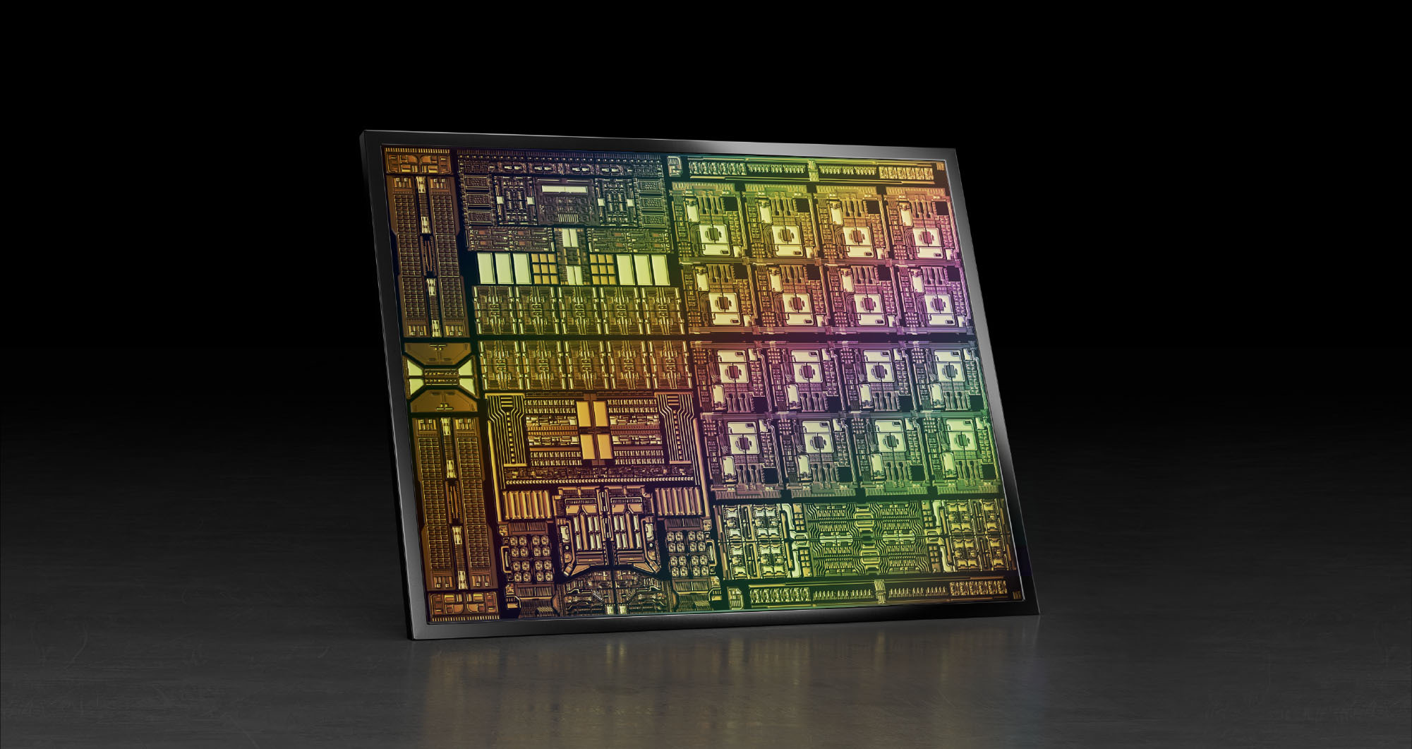
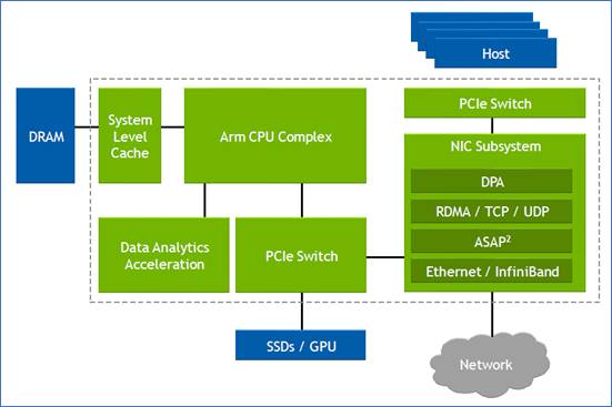


 Eitan MedinaGoya, the start-up’s second device, is an inference processor that implements the optimised, trained neural network.
 Source: Habana Labs
 The Goya IC architecture. Habana says this is a general representation of the chip and what is shown is not the actual number of tensor processor cores (TPCs). Source: Habana Labs