
Marvell plans for CXL's introduction in the data centre

The open interconnect Compute Express Link (CXL) standard promises to change how data centre computing is architected.
CXL enables the rearrangement of processors (CPUs), accelerator chips, and memory within computer servers to boost efficiency.
“CXL is such an important technology that is in high focus today by all the major cloud hyperscalers and system OEMs,” says Thad Omura, vice president of flash marketing at Marvell.
Semiconductor firm Marvell has strengthened its CXL expertise by acquiring Tanzanite Silicon Solutions.
Tanzanite was the first company to show two CPUs sharing common memory using a CXL 2.0 controller implemented using a field-programmable gate array (FPGA).
Marvell intends to use CXL across its portfolio of products.
Terms of the deal for the 40-staff Tanzanite acquisition have not been disclosed.
Data centre challenges
Memory chips are the biggest item spend in a data centre. Each server CPU has its own DRAM, the fast volatile memory overseen by a DRAM controller. When a CPU uses only part of the memory, the rest is inactive since other server processors can’t access it.
“That’s been a big issue in the industry; memory has consistently been tied to some sort of processor,” says Omura.
Maximising processing performance is another issue. Memory input-output (I/O) performance is not increasing as fast as processing performance. Memory bandwidth available to a core has thus diminished as core count per CPU has increased. “These more powerful CPU cores are being starved of memory bandwidth,” says Omura.
CXL tackles both issues: it enables memory to be pooled improving usage overall while new memory data paths are possible to feed the cores.
CXL also enables heterogeneous compute elements to share memory. For example, accelerator ICs such as graphic processing units (GPUs) working alongside the CPU on a workload.
CXL technology
CXL is an industry-standard protocol that uses the PCI Express (PCIe) bus as the physical layer. PCI Express is used widely in the data centre; PCIe 5.0 is coming to market, and the PCIe 6.0 standard, the first to use 4-level pulse-amplitude modulation (PAM-4), was completed earlier this year.
In contrast, other industry interface protocols such as OpenCAPI (open coherent accelerator processor interface) and CCIX (cache coherent interconnect for accelerators) use custom physical layers.
“The [PCIe] interface feeds are now fast enough to handle memory bandwidth and throughput, another reason why CXL makes sense today,” says Omura.
CXL supports low-latency memory transactions in the tens of nanoseconds. In comparison, the non-volatile memory express storage (NVMe), which uses a protocol stack run on a CPU, has tens of microseconds transaction times.
“The CXL protocol stack is designed to be lightweight,” says Omura. “It doesn’t need to go through the whole operating system stack to get a transaction out.”
CXL enables cache coherency, which is crucial since it ensures that the accelerator and the CPU see the same data in a multi-processing system.
Memory expansion
The first use of CXL will be to simplify the adding of memory.
A server must be opened when adding extra DRAM using a DIMM (dual in-line memory module). And there are only so many DIMM slots in a server.
The DIMM also has no mechanism to pass telemetry data such as its service and bit-error history. Cloud data centre operators use such data to oversee their infrastructure.
Using CXL, a memory expander module can be plugged into the front of the server via PCIe, avoiding having to open the server. System cooling is also more straightforward since the memory is far from the CPU. The memory expander’s CXL controller can also send telemetry data.
CXL also boosts memory bandwidth. When adding a DIMM to a CPU, the original and added DIMM share the same channel; capacity is doubled but not the interface bandwidth. Using CXL however opens a channel as the added memory uses the PCIe bus.
“If you’re using the by-16 ports on a PCIe generation five, it [the interface] exceeds the [DRAM] controller bandwidth,” says Omura.
Pooled memory
CXL also enables memory pooling. A CPU can take memory from the pool for a task, and when completed, it releases the memory so that another CPU can use it. Future memory upgrades are then added to the pool, not an individual CPU. “That allows you to scale memory independently of the processors,” says Omura.
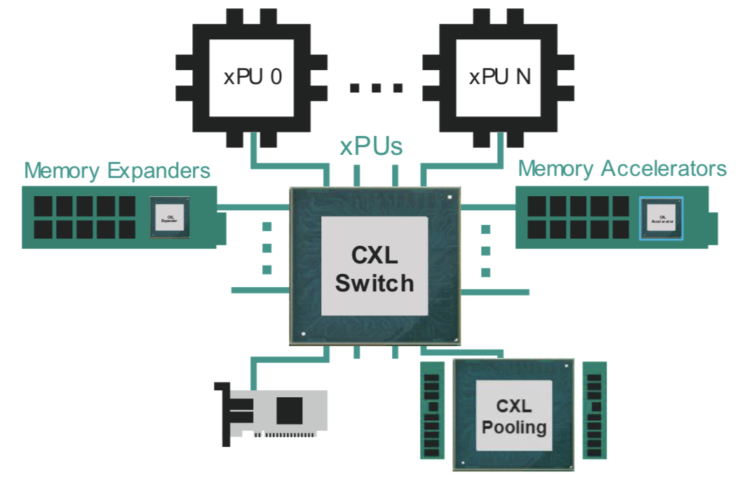
The likely next development is for all the CPUs to access memory via a CXL switch. Each CPU will no longer needs a local DRAM controller but rather it can access a memory expander or the memory pool using the CXL fabric (see diagram above).
Going through a CXL switch adds latency to the memory accesses. Marvell says that the round trip time for a CPU to access its local memory is about 100ns, while going through the CXL switch to pooled memory is projected to take 140-160ns.
The switch can also connect a CXL accelerator. Here, an accelerator IC is added to memory which can be shared in a cache coherent manner with the CPU through the switch fabric (see diagram above).
I/O acceleration hardware can also be added using the CXL switch. Such hardware includes Ethernet, data processing unit (DPU) smart network interface controllers (smartNICs), and solid-state drive (SSD) controllers.
“Here, you are focused on accelerating protocol-level processing between the network device or between the CPU and storage,” says Omura. These I/O devices become composable using the CXL fabric.
More CXL, less Ethernet
Server boxes in the data are stacked. Each server comprises CPUs, memory, accelerators, network devices and storage. The servers talk to each other via Ethernet and other server racks using a top-of-rack switch.
But the server architecture will change as CXL takes hold in the data centre.

“As we add CXL into the infrastructure, for the first time, you’re going to start to see disaggregate memory,” says Omura. “You will be able to dynamically assign memory resources between servers.”
For some time yet, servers will have dedicated memory. Eventually, however, the architecture will become disaggregated with separate compute, memory and I/O racks. Moreover, the interconnect between the boxes will be through CXL. “Some of the same technology that has been used to transmit high-speed Ethernet will also be used for CXL,” says Omura.
Omura says deployment of the partially-disaggregated rack will start in 2024-25, while complete disaggregation will likely appear around the decade-end.
Co-packaged optics and CXL
Marvell says co-packaging optics will fit well with CXL.

“As you disaggregate memory from the CPU, there is a need to have electro-optics drive distance and bandwidth requirements going forward,” says Nigel Alvares, vice president of solutions marketing at Marvell.
However, CXL must be justified from a cost and latency standpoint, limiting its equipment-connecting span.
“The distance in which you can transmit data over optics versus latency and cost is all being worked out right now,” says Omura. The distance is determined by the transit time of light in fibre and the forward error correction scheme used.
But CXL needs to remain very low latency because memory transactions are being done over it, says Omura: “We’re no longer fighting over just microseconds or milliseconds of networking, now we’re fighting over nanoseconds.”
Marvell can address such needs with its acquisition of Inphi and its PAM-4 and optical expertise, the adoption of PAM-4 encoding for PCIe 6.0, and now the addition of CXL technology.

Marvell's first Inphi chips following its acquisition

Marvell unveiled three new devices at the recent OFC virtual conference and show.
One chip is its latest coherent digital signal processor (DSP), dubbed Deneb. The other two chips, for use within the data centre, are a PAM-4 (4-level pulse-amplitude modulation) DSP, and a 1.6-terabit Ethernet physical layer device (PHY).
The chips are Marvell’s first announced Inphi products since it acquired the company in April. Inphi’s acquisition adds $0.7 billion to Marvell’s $3 billion annual revenues while the more than 1,000 staff brings the total number of employees to 6,000.
Marvell spends 30 per cent of its revenues on R&D.
Acquisitions
Inphi is the latest of a series of Marvell acquisitions as it focusses on data infrastructure.
Marvell acquired two custom ASIC companies in 2019: Avera Semiconductor, originally the ASIC group of IBM Microelectronics, and Aquantia that has multi-gigabit PHY expertise.
A year earlier Marvell acquired processing and security chip player, Cavium Networks. Cavium had acquired storage specialist, QLogic, in 2017.
These acquisitions have more than doubled Marvell’s staff. Inphi brings electro-optics expertise for the data centre and optical transport and helps Marvell address the cloud and on-premises data centre markets as well as the 5G carrier market.
Marvell is also targeting the enterprise/ campus market and what it highlights as a growth area, automotive. Nigel Alvares, vice president of solutions at Marvell, notes the growing importance of in-vehicle networking, what he calls a ‘data-centre-on-wheels’.
“Inphi’s technology could also help us in automotive as optical technologies are used for self-driving initiatives in future,” says Alvares.
Inphi also brings integration, co-packaging and multi-chip module expertise.

Merchant chip and custom ASIC offerings
Cloud operators and 5G equipment vendors are increasingly developing custom chip designs. Marvell says it is combining its portfolio with their intellectual property (IP) to develop and build custom ICs.
Accordingly, in addition to its merchant chips such as the three OFC-announced devices, Marvell partners with cloud players or 5G vendors, providing them with key IP blocks that are integrated with their custom IP. Marvell can also build the ASICs.
Another chip-design business model Marvell offers is the integration of different hardware in a multi-chip package. The components include a custom ASIC, merchant silicon, high-speed memory and third-party chiplets.
“We co-package and deliver it to a cloud hyperscaler or a 5G technical company,” says Alvares.
Marvell says this chip strategy serves two market sectors: the cloud hyperscalers and the telcos.
Cloud players are developing custom solutions as they become more vertically integrated. They also have deep pockets. But they can’t do everything because they are not chip experts so they partner with companies like Marvell.
“The five to 10 hyperscalers in the world, they are doing so much creative stuff to optimise applications that they need custom silicon,” says Alvares.
The telcos, in contrast, are struggling to grow their revenues and favour merchant ICs, given they no longer have the R&D budgets of the past. It is this split in the marketplace which Marvell is targeting its various chip services.
OFC announcements
At OFC, Marvell announced the Deneb coherent DSP, used for optical transport including the linking of equipment between data centres.
The Deneb DSP is designed with open standards in mind and complements the 400-gigabit CMOS Canopus DSP announced by Inphi in 2019.
Deneb adds the oFEC forward error correction scheme to support open standards such as OpenZR+, 100-gigabit ZR, the 400-gigabit OpenROADM MSA and CableLabs’ 100-gigabit standard.
The 100-gigabit ZR is targeted at the 5G access market and mobile backhaul. Like the OIF 400G ZR, it supports reaches of 80-120km but uses quadrature phase-shift keying (QPSK) modulation.
“Not only do we support 100 gigabit [coherent] but we also have added the full industrial temperature range, from -40oC to 85oC,” says Michael Furlong, associated vice president, product marketing at Marvell.
The Deneb DSP is sampling now. Both the Deneb and Canopus DSPs will have a role in the marketplace, says Furlong.

Atlas PAM-4 DSP and the 1.6-terabit PHY
Marvell also announced at OFC the Atlas PAM-4 DSP and a dual 800-gigabit PHY devices used within the data centre.
Atlas advances Marvell’s existing family of Polaris PAM-4 DSPs in that it integrates physical media devices. “We are integrating [in CMOS] the trans-impedance amplifier (TIA) and laser drivers,” says Alvares.
Using the 200-gigabit Atlas reduces an optical module design from three chips to two; the Atlas comprises a transmit chip and a receiver chip (see diagram below). Using the Atlas chips reduces the module’s bill of materials, while power consumption is reduced by a quarter.

The Atlas chips, now sampling, are not packaged but offered as bare die and will be used for 200-gigabit SR4 and FR4 modules. Meanwhile, Marvell’s 1.6-terabit PHY – the 88X93160, – is a dual 800-gigabit copper DSP that performs retimer and gearbox functions.
“We view this as the key data centre building block for the next decade,” says Alvares. “The world is just starting to design 100-gigabit serial for their infrastructure.”
The device, supporting 16, 100-gigabit lanes, is the industry’s first 100-gigabit serial retimer, says Marvell. The device drives copper cable and backplanes and is being adopted for links between the server and the top-of-tack switch or to connect switches in the data centre.
The device is suitable for next-generation 400-gigabit and 800-gigabit Ethernet links that use 100-gigabit electrical serialisers-deserialisers (serdes).
The 5nm CMOS device supports over a 38dB (decibel) link budget and reduces I/O power by 40 per cent compared to a 50-gigabit Nigel PAM4-based PHY.
The 100-gigabit serdes design will also be used with Marvell’s Prestera switch portfolio.

Marvell exploits 5nm CMOS to add Octeon 10 DPU smarts

The Octeon family has come a long way since the networking infrastructure chip was introduced by Cavium Networks in 2005.
Used for data centre switches and routers, the original chip family featured 1 to 16, 64-bit MIPS cores and hardware acceleration units for packet processing and encryption. The devices were implemented using foundry TSMC’s 130nm CMOS process.
Marvell, which acquired Cavium in 2018, has taped out the first two devices of its latest, seventh-generation Octeon 10 family.
The devices, coined data processing units (DPU), will feature up to 36 state-of-the-art ARM cores, support a 400-gigabit line rate, 1 terabit of switching capacity, and dedicated hardware for machine-learning and vector packet processing (VPP).
Marvell is using TSMC’s latest 5nm CMOS process to cram all these functions on the DPU system-on-chip.
The 5nm-implemented Octeon 10 coupled with the latest ARM cores and improved interconnect fabric will triple data processing performance while halving power consumption compared to the existing Octeon TX2 DPU.
DPUs join CPUs and GPUs
The DPU is not a new class of device but the term has become commonplace for a processor adept at computing and moving and processing packets.
Indeed, the DPU is being promoted as a core device in the data centre alongside central processing units (CPUs) and graphic processing units (GPUs).
As Marvell explains, a general-purpose CPU can perform any processing task but it doesn’t have the computational resources to meet all requirements. For certain computationally-intensive tasks like graphics and artificial intelligence, for example, the GPU is far more efficient.
The same applies to packet processing. The CPU can perform data-plane processing tasks but it is inefficient when it comes to intensive packet processing, giving rise to the DPU.
“The CPU is just not effective from a total cost of ownership, power and performance point of view,” says Nigel Alvares, vice president of solutions marketing at Marvell.
Data-centric tasks
The DPU is used for smart network interface controller (SmartNIC) cards found in computer servers. The DPU is also suited for standalone tasks at the network edge and for 5G.
Marvell says the Octeon DPU can be used for data centres, 5G wireless transport, SD-WAN, and fanless boxes for the network edge.
Data centre computation is moving from application-centric to more data-centric tasks, says Marvell. Server applications used to host all the data they needed when executing algorithms. Now applications gather data from various compute clusters and locations.
“The application doesn’t have all the data but there is a lot of data that needs to be pumped into the application from many points,” says Jeffrey Ho, senior product manager at Marvell. “So a lot of network overlay, a lot of East-West traffic.”
This explains the data-centric nature of tasks or, as Ho describes it, the data centre appearing as a mesh of networks: “It’s a core network, it is a router network, it is an enterprise network – all in one block.”
Octeon 10 archtecture
The Octeon 10 family uses ARM’s latest core architecture, the Neoverse N2 processor, Arm’s first Armv9 Infrastructure CPU, for general-purpose computational tasks. Each ARM core has access to hierarchical cache memory and external DDR5 SDRAM memory.
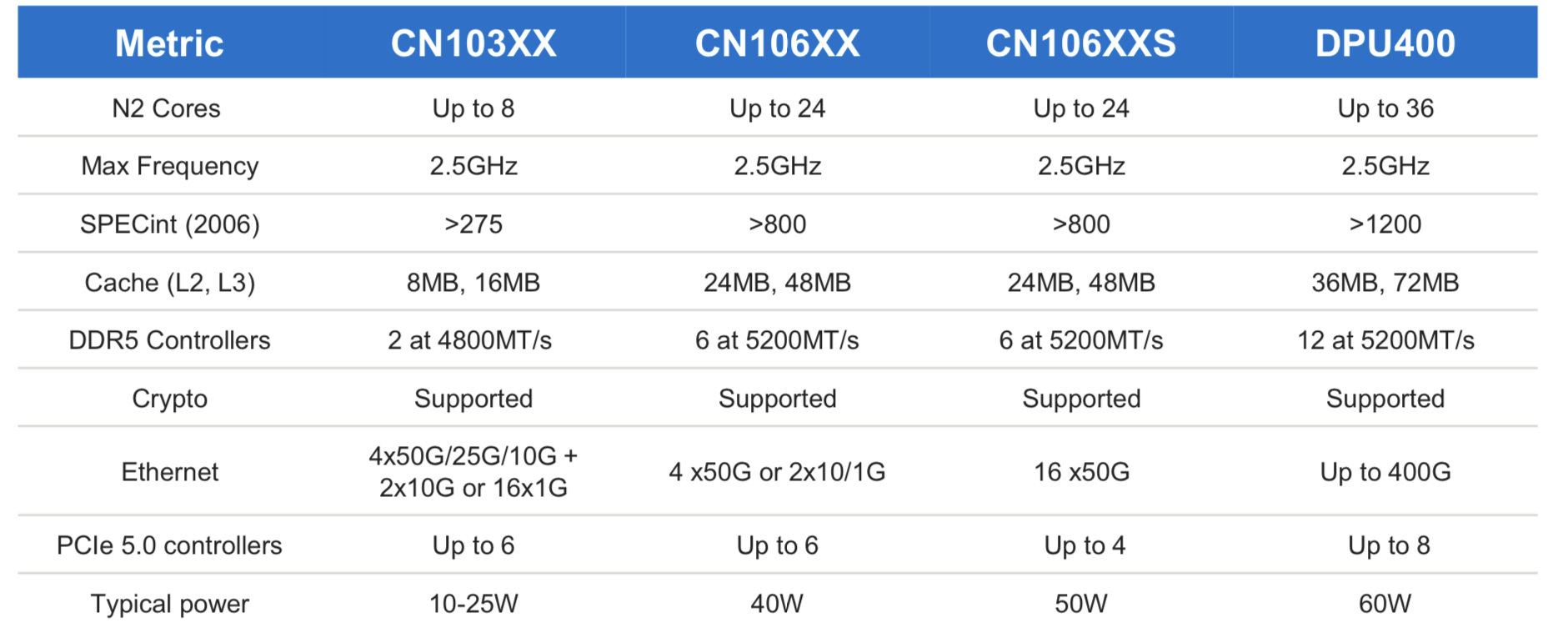
The initial Octeon 10 family members range from the CN103XX which has up to eight ARM N2 cores, each with Level 1 and private Level 2 cache and shared level 2 and 3 caches (8MB and 16MB, respectively).
The most powerful DPU of the Octeon 10 family is the DPU400 which will have up to 36 ARM cores and 36MB level 2 and 72MB level 3 caches.
“Then you have the acceleration hardware that is very friendly to this generic compute,” says Ho.
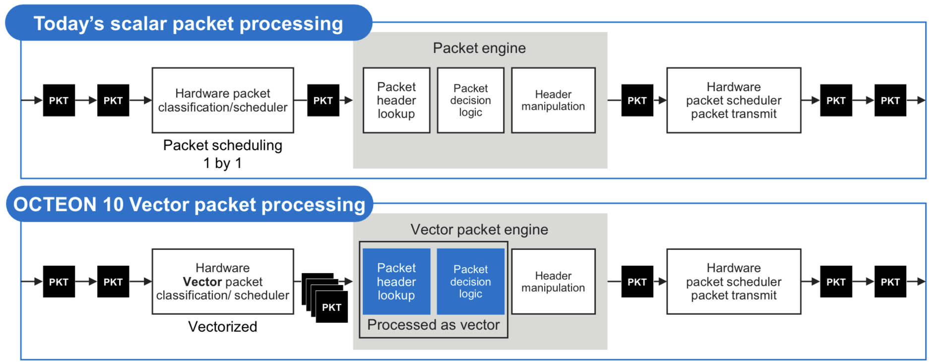
One custom IP block is for vector packet processing (VPP). VPP has become popular since becoming available as open-source software that batch-processes packets with similar attributes. Marvell says that until now, the hardware processed the packets one at a time such that the potential of VPP has not been fully realised.
The Octean 10 is the first device family to feature hardware for VPP acceleration. Accordingly, only one look-up table operation and one logical decision may be required before header manipulation is performed for each of the grouped packets. The specialised hardware accelerates VPP by between 3-5x.
The DPU also integrates on-chip hardware for machine-learning inferencing tasks.
Machine learning can be applied to traffic patterns on a compute cluster such that every day or so, newly learned models can be downloaded onto the DPU for smart malware detection. This is learnt behaviour; no rules need be written in code, says Marvell. Machine learning can determine if a packet is malware to an accuracy of 80 per cent, says Ho.
The hardware can even identify suspect packets by learning application types even when the packets themselves are encrypted using the IPSec protocol.
The DPU’s machine learning inference hardware can also be used for other tasks such as beamforming optimisation in cellular networks.
As for the 400-gigabit rating of the Octeon DPU, this is the maximum input and output that a CPU can cope with if every packet needs processing. And when each packet passes through the IPsec encyption engines, the maximum line rate is 400 gigabits.
In turn, if a packet need not pass through the CPU or no cryptography is required, one terabit of Layer 2/ Layer 3 switching can be done on-chip.
“All these are separate accelerator capability of the platform,” says Ho. The data path bandwidth of the DPU is 400Gbps+, IPSec throughput is 400Gbps+, and the switch capability is 1 terabit.”
Using software, the DPU accelerators are configured according to the data processing needs which may use all or some of the on-chip accelerators, he says.

4G and 5G cellular systems
For radio access networks, the radio head units talk to a distributed unit (DU) and a centralised unit (CU). (See diagram.)

The DU chassis houses six or eight line cards typically. The DU has a main controller that connects all the signals and backhauls them to the CU. This requires a two-chip solution with a switch chip next to each Octeon.
Using a 5nm process, the switch-integrated Octeon DPU reduces the DU’s overall power consumption and bill of materials. This Octeon DPU can be used for the DU, the fronthaul gateway and even the CU.
The DPU also exploits the 1-terabit switching capacity for the DU chassis example. Here, six Octeon Fusion-O chips, which perform Layer 1 processing, are connected to six radio units. Each of the six Fusion-O chips connects to the DPU via a 50-gigabit serialiser/ deserialiser (serdes).
Typical DU designs may use two Octeon DPUs, the second being a standby host DPU. This accounts for six line cards and two Octeon DPUs per DU chassis.
Market status
Marvell says that for 100-gigabit-throughput DPUs, up to 60 per cent of volumes shipped are used in the cloud and 40 per cent at the network edge.
Since throughput rates in the cloud are growing faster than the network edge, as reflected with the advent of 200- and 400-gigabit SmartNIC cards, the overall ratio of devices used for the cloud will rise.
The first two Octeon 10 devices taped out two months ago were the CN106XX and CN106XXS. These devices will sample in the second half of 2021.
The two will be followed by the CN103XX which is expected around spring 2022 and following that will be the DPU400.