
Nvidia's plans for the data processor unit
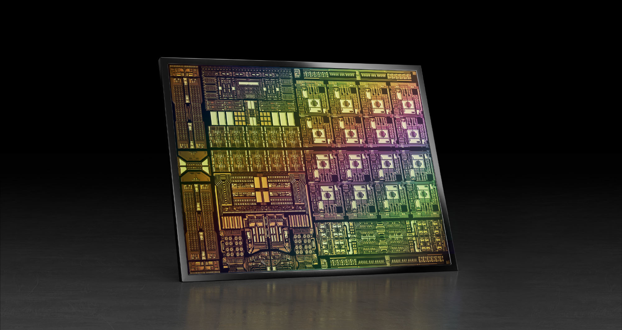
When Nvidia’s CEO, Jensen Huang, discussed its latest 400-gigabit BlueField-3 data processing unit (DPU) at the company’s 2021 GTC event, he also detailed its successor.
Companies rarely discuss chip specifications two generations ahead; the BlueField-3 only begins sampling next quarter.
The BlueField-4 will advance Nvidia’s DPU family.
It will double again the traffic throughput to 800 gigabits-per-second (Gbps) and almost quadruple the BlueField-3’s integer processing performance.
But one metric cited stood out. The BlueField-4 will increase by nearly 1000x the number of terabit operators-per-second (TOPS) performed: 1,000 TOPS compared to the BlueField-3’s 1.5 TOPS.
Huang said artificial intelligence (AI) technologies will be added to the BlueField-4, implying that the massively parallel hardware used for Nvidia’s graphics processor units (GPUs) are to be grafted onto its next-but-one DPU.
Why add AI acceleration? And will it change the DPU, a relatively new processor class?
Data processor units
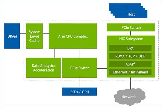
Nvidia defines the DPU as a programmable device for networking.
The chip combines general-purpose processing – multiple RISC cores used for control-plane tasks and programmed in a high-level language – with accelerator units tailored for packet-processing data-plane tasks.
“The accelerators perform functions for software-defined networking, software-defined storage and software-defined security,” says Kevin Deierling, senior vice president of networking at Nvidia.
The DPU can be added to a Smart Network Interface Card (SmartNIC) that complements the server’s CPU, taking over the data-intensive tasks that would otherwise burden the server’s most valuable resource.
Other customers use the DPU as a standalone device. “There is no CPU in their systems,” says Deierling.
Storage platforms is one such example, what Deierling describes as a narrowly-defined workload. “They don’t need a CPU and all its cores, what they need is the acceleration capabilities built into the DPU, and a relatively small amount of compute to perform the control-path operations,” says Deierling.
Since the DPU is the server’s networking gateway, it supports PCI Express (PCIe). The PCIe bus interfaces to the host CPU, to accelerators such as GPUs, and supports NVMe storage. NVMe is a non-volatile memory host controller interface specification.
BlueField 3
When announced in 2021, the 22-billion transistor BlueField-3 chip was scheduled to sample this quarter. “We need to get the silicon back and do some testing and validation before we are sampling,” says Deierling.
The device is a scaled-up version of the BlueField-2: it doubles the throughput to 400Gbps and includes more CPU cores: 16 Cortex-A78 64-bit ARM cores.
Nvidia deliberately chose not to use more powerful ARM cores. “The ARM is important, there is no doubt about it, and there are newer classes of ARM,” says Deierling. “We looked at the power and the performance benefits you’d get by moving to one of the newer classes and it doesn’t buy us what we need.”
The BlueField-3 has the equivalent processing performance of 300 X86 CPU cores, says Nvidia, but this is due mainly to the accelerator units, not the ARM cores.
The BlueField-3 input-output [I/O] includes Nvidia’s ConnectX-7 networking unit that supports 400 Gigabit Ethernet (GbE) which can be split over 1, 2 or 4 ports. The DPU also doubles the InfiniBand interface compared to the BlueField-2, either a single 400Gbps (NDR) port or two 200Gbps (HDR) ports. There are also 32 lanes of PCI Express 5.0, each lane supporting 32 giga-transfers-per-second (GT/s) in each direction.
The memory interface is two DDR5 channels, doubling both the memory performance and the channel count of the BlueField-2.
The data path accelerator (DPA) of the BlueField-3 comprises 16 cores, each supporting 16 instruction threads. Typically, when a packet arrives, it is decrypted and the headers are inspected after which the accelerators are used. The threads are used if the specific function needed is not accelerated. Then, a packet is assigned to a thread and processed.
“The DPA is a specialised part of our acceleration core that is highlighly programmable,” says Deierling.
Other programmable logic blocks include the accelerated switching and packet processing (ASAP2) engine that parses packets. It inspects packet fields looking for a match that tells it what to do, such as dropping the packet or rewriting its header.
In-line acceleration
The BlueField-3 implements the important task of security.
A packet can have many fields and encapsulations. For example, the fields can include a TCP header, quality of service, a destination IP and an IP header. These can be encapsulated into an overlay such as VXLAN and further encapsulated into a UDP packet before being wrapped in an outer IP datagram that is encrypted and sent over the network. Then, only the IPSec header is exposed; the remaining fields are encrypted.
Deierling says the BlueField-3 does the packet encryption and decryption in-line.
For example, the DPU uses the in-line IPsec decode to expose the headers of the various virtual network interfaces – the overlays – of a received packet. Picking the required overlay, the packet is sent to a set of service-function chainings that use all the accelerators available such as tackling distributed denial-of-service and implementing a firewall and load balancing.
“You can do storage, you can do an overlay, receive-side scaling [RSS], checksums,” says Deierling. “All the accelerations built into the DPU become available.”
Without in-line processing, the received packet goes through a NIC and into the memory of the host CPU. There, it is encrypted and hence opaque; the packet’s fields can’t benefit from the various acceleration techniques. “It is already in memory when it is decrypted,” says Deierling.
Often, with the DPU, the received packet is decrypted and passed to the host CPU where the full packet is visible. Then, once the host application has processed the data, the data and packet may be encrypted again before being sent on.
“In a ‘zero-trust’ environment, there may be a requirement to re-encrypt the data before sending it onto the next hop,” says Deierling. “In this case, we just reverse the pipeline.”
An example is confidential healthcare information where data needs to be encrypted before being sent and stored.
DPU evolution
There are many application set to benefit from DPU hardware. These cover the many segments Nvidia is addressing including AI, virtual worlds, robotics, self-driving cars, 5G and healthcare.
All need networking, storage and security. “Those are the three things we do but it is software-defined and hardware-accelerated,” says Deierling.
Nvidia has an ambitious target of launching a new DPU every 18 months. That suggests the BlueField-4 could sample as early as the end of 2023.
The 800-gigabit Bluefield-4 will have 64-billion transistors and nearly quadruple the integer processing performance of the BlueField-3: from 42 to 160 SPECint.
Nvidia says its DPUs, including the BlueField-4, are evolutionary in how they scale the ARM cores, accelerators and throughput. However, the AI acceleration hardware added to the BlueField-4 will change the nature of the DPU.
“What is truly salient is that [1,000] TOPS number,” says Deierling. “And that is an AI acceleration; that is leveraging capabilities Nvidia has on the GPU side.”
Self-driving cars, 5G and robotics
An AI-assisted DPU will support such tasks as video analytics, 5G and robotics.
For self-driving cars, the DPU will reside in the data centre, not in the car. But that too will change.“Frankly, the car is becoming a data centre,” notes Deierling.
Deep learning currently takes place in the data centre but as the automotive industry adopts Ethernet, a car’s sensors – lidar, radar and cameras – will send massive amounts of data which an IC must comprehend.
This is relevant not just for automotive but all applications where data from multiple sensors needs to be understood.
Deierling describes Nvidia as an AI-on-5G company.
“We have a ton of different things that we are doing and for that, you need a ton of parallel-processing capabilities,” he says. This is why the BlueField-4 is massively expanding its TOPS rating.
He describes how a robot on an automated factory floor will eventually understand its human colleagues.
“It is going to recognize you as a human being,“ says Deierling. “You are going to tell it: ‘Hey, stand back, I’m coming in to look at this thing’, and the robot will need to respond in real-time.”
Video analytics, voice processing, and natural language processing are all needed while the device will also be running a 5G interface. Here, the DPU will reside in a small mobile box: the robot.
“Our view of 5G is thus more comprehensive than just a fast pipe that you can use with a virtual RAN [radio access network] and Open RAN,” says Deierling. “We are looking at integrating this [BlueField-4] into higher-level platforms.”

Compute vendors set to drive optical I/O innovation

Part 2: Data centre and high-performance computing trends
Professor Vladimir Stojanovic has an engaging mix of roles.
When he is not a professor of electrical engineering and computer science at the University of California, Berkeley, he is the chief architect at optical interconnect start-up, Ayar Labs.
Until recently Stojanovic spent four days each week at Ayar Labs. But last year, more of his week was spent at Berkeley.
Stojanovic is a co-author of a 2015 Nature paper that detailed a monolithic electronic-photonics technology. The paper described a technological first: how a RISC-V processor communicated with the outside world using optical rather than electronic interfaces.
It is this technology that led to the founding of Ayar Labs.
Research focus
“We [the paper’s co-authors] always thought we would use this technology in a much broader sense than just optical I/O [input-output],” says Stojanovic.
This is now Stojanovic’s focus as he investigates applications such as sensing and quantum computing. “All sorts of areas where you can use the same technology – the same photonic devices, the same circuits – arranged in different configurations to achieve different goals,” says Stojanovic.
Stojanovic is also looking at longer-term optical interconnect architectures beyond point-to-point links.
Ayar Labs’ chiplet technology provides optical I/O when co-packaged with chips such as an Ethernet switch or an “XPU” – an IC such as a CPU or a GPU (graphics processing unit). The optical I/O can be used to link sockets, each containing an XPU, or even racks of sockets, to form ever-larger compute nodes to achieve “scale-out”.
But Stojanovic is looking beyond that, including optical switching, so that tens of thousands or even hundreds of thousands of nodes can be connected while still maintaining low latency to boost certain computational workloads.
This, he says, will require not just different optical link technologies but also figuring out how applications can use the software protocol stack to manage these connections. “That is also part of my research,” he says.
Optical I/O
Optical I/O has now become a core industry focus given the challenge of meeting the data needs of the latest chip designs. “The more compute you put into silicon, the more data it needs,” says Stojanovic.
Within the packaged chip, there is efficient, dense, high-bandwidth and low-energy connectivity. But outside the package, there is a very sharp drop in performance, and outside the chassis, the performance hit is even greater.
Optical I/O promises a way to exploit that silicon bandwidth to the full, without dropping the data rate anywhere in a system, whether across a shelf or between racks.
This has the potential to build more advanced computing systems whose performance is already needed today.
Just five years go, says Stojanovic, artificial intelligence (AI) and machine learning were still in their infancy and so were the associated massively parallel workloads that required all-to-all communications.
Fast forward to today, such requirements are now pervasive in high-performance computing and cloud-based machine-learning systems. “These are workloads that require this strong scaling past the socket,” says Stojanovic.
He cites natural language processing that within 18 months has grown 1000x in terms of the memory required; from hosting a billion to a trillion parameters.
“AI is going through these phases: computer vision was hot, now it’s recommender models and natural language processing,” says Stojanovic. “Each generation of application is two to three orders of magnitude more complex than the previous one.”
Such computational requirements will only be met using massively parallel systems.
“You can’t develop the capability of a single node fast enough, cramming more transistors and using high-bandwidth memory,“ he says. High-bandwidth memory (HBM) refers to stacked memory die that meet the needs of advanced devices such as GPUs.
Co-packaged optics
Yet, if you look at the headlines over the last year, it appears that it is business as usual.
For example, there have been a Multi Source Agreement (MSA) announcement for new 1.6-terabit pluggable optics. And while co-packaged optics for Ethernet switch chips continues to advance, it remains a challenging technology; Microsoft has said it will only be late 2023 when it starts using co-packaged optics in its data centres.
Stojanovic stresses there is no inconsistency here: it comes down to what kind of bandwidth barrier is being solved and for what kind of application.
In the data centre, it is clear where the memory fabric ends and where the networking – implemented using pluggable optics – starts. That said, this boundary is blurring: there is a need for transactions between many sockets and their shared memory. He cites Nvidia’s NVLink and AMD’s Infinity Fabric links as examples.
“These fabrics have very different bandwidth densities and latency needs than the traditional networks of Infiniband and Ethernet,” says Stojanovic. “That is where you look at what physical link hardware answers the bottleneck for each of these areas.”
Co-packaged optics is focussed on continuing the scaling of Ethernet switch chips. It is a more scalable solution than pluggables and even on-board optics because it eliminates long copper traces that need to be electrically driven. That electrical interface has to escape the switch package, and that gives rise to that package-bottleneck problem, he says.
There will be applications where pluggables and on-board optics will continue to be used. But they will still need power-consuming retimer chips and they won’t enable architectures where a chip can talk to any other chip as if they were sharing the same package.
“You can view this as several different generations, each trying to address something but the ultimate answer is optical I/O,” says Stojanovic.
How optical connectivity is used also depends on the application, and it is this diversity of workloads that is challenging the best of the system architects.
Application diversity
Stojanovic cites one machine learning approach for natural language processing that Google uses that scales across many compute nodes, referred to as the ‘multiplicity of experiments’ (MoE) technique.
A processing pipeline is replicated across machines, each performing part of the learning. For the algorithm to work in parallel, each must exchange its data set – its learning – with every other processing pipeline, a stage referred to as all-to-all dispatch and combine.
“As you can imagine, all-to-all communications is very expensive,” says Stojanovic. “There is a lot of data from these complex, very large problems.”
Not surprisingly, as the number of parallel nodes used grows, a greater proportion of the overall time is spent exchanging the data.
Using 1,000 AI processors running 2,000 experiments, a third of the time is required for data exchange. Scaling the hardware to 3,000 to 4,000 AI processors and communications dominate the runtime.
This, says Stojanovic, is a very interesting problem to have: it’s an example where adding more compute simply does not help.
“It is always good to have problems like this,” he says. “You have to look at how you can introduce some new technology that will be able to resolve this to enable further scaling, to 10,000 or 100,000 machines.”
He says such examples highlight how optical engineers must also have an understanding of systems and their workloads and not just focus on ASIC specifications such as bandwidth density, latency and energy.
Because of the diverse workloads, what is needed is a mixture of circuit switching and packet switching interconnect.
Stojanovic says high-radix optical switching can connect up to a thousand nodes and, scaling to two hops, up to a million nodes in sub-microsecond latencies. This suits streamed traffic.

But an abundance of I/O bandwidth is also needed to attach to other types of packet switch fabrics. “So that you can also handle cache-line size messages,” says Stojanovic.
These are 64 bytes long and are found with processing tasks such as Graph AI where data searches are required, not just locally but across the whole memory space. Here, transmissions are shorter and involve more random addressing and this is where point-to-point optical I/O plays a role.
“It is an art to architect a machine,” says Stojanovic.
Disaggregation
Another data centre trend is server disaggregation which promises important advantages.
The only memory that meets the GPU requirements is HBM. But it is becoming difficult to realise taller and taller HBM stacks. Stojanovic cites as an example how Nvidia came out with its A100 GPU with 40GB of HBM that was quickly followed a year later, by an 80GB A100 version.
Some customers had to do a complete overall of their systems to upgrade to the newer A100 yet welcomed the doubling of memory because of the exponential growth in AI workloads.
By disaggregating a design – decoupling the compute and memory into separate pools – memory can be upgraded independently of the computing. In turn, pooling memory means multiple devices can share the memory and it avoids ‘stranded memory’ where a particular CPU is not using all its private memory. Having a lot of idle memory in a data centre is costly.
If the I/O to the pooled memory can be made fast enough, it promises to allow GPUs and CPUs to access common DDR memory.
“This pooling, with the appropriate memory controller design, equalises the playing field of GPUs and CPUs being able to access jointly this resource,” says Stojanovic. “That allows you to provide way more capacity – several orders more capacity of memory – to the GPUs but still be within a DRAM read access time.”
Such access time is 50-60ns overall from the DRAM banks and through an optical I/O. The pooling also means that the CPUs no longer have stranded memory.
“Now something that is physically remote can be logically close to the application,” says Stojanovic.
Challenges
For optical I/O to enable such system advances what is needed is an ecosystem of companies. Adding an optical chiplet alongside an ASIC is not the issue; chiplets are aready used by the chip industry. Instead, the ecosystem is needed to address such practical matters as attaching fibres and producing the lasers needed. This requires collaboration among companies across the optical industry.
“That is why the CW-WDM MSA is so important,” says Stojanovic. The MSA defines the wavelength grids for parallel optical channels and is an example of what is needed to launch an ecosystem and enable what system integrators and ultimately the hyperscalers want to do.
Systems and networking
Stojanovic concludes by highlighting an important distinction.
The XPUs have their own design cycles and, with each generation, new features and interfaces are introduced. “These are the hearts of every platform,” says Stojanovic. Optical I/O needs to be aligned with these devices.
The same applies to switch chips that have their own development cycles. “Synchronising these and working across the ecosystem to be able to find these proper insertion points is key,” he says.
But this also implies that the attention given to the interconnects used within a system (or between several systems i.e. to create a larger node) will be different to that given to the data centre network overall.
“The data centre network has its own bandwidth pace and needs, and co-packaged optics is a solution for that,“ says Stojanovic. “But I think a lot more connections get made, and the rules of the game are different, within the node.”
Companies will start building very different machines to differentiate themselves and meet the huge scaling demands of applications.
“There is a lot of motivation from computing companies and accelerator companies to create node platforms, and they are freer to innovate and more quickly adopt new technology than in the broader data centre network environment,” he says
When will this become evident? In the coming two years, says Stojanovic.